Contents
What is HDI PCB?
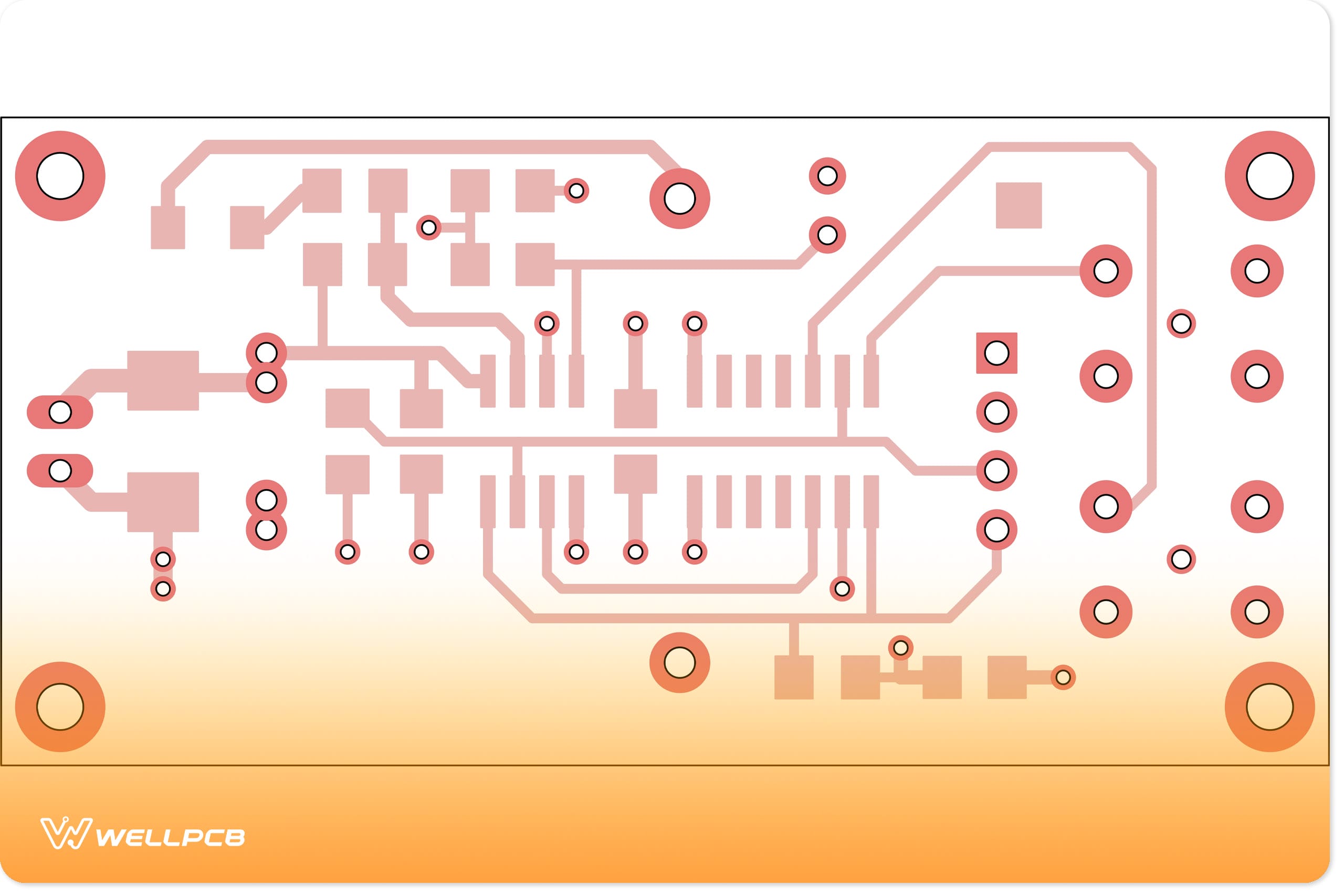
Electronic devices with lighter, thinner, and smaller designs have endorsed PCBs to become more advanced so that High-Density Interconnection (HDI) PCBs arose and took place in the industry. The main difference between HDI PCBs and traditional ones is that they provide high density because they employ micro-via layers.
The foundations for interconnection of various circuit board Making. THE conventional PCB routing methods can not achieve this. With HDI, PCB layers are micro-vias layers with small diameters and depths of 50 to 150μm, respectively. They allow small and thin HDI PCBs to manufacture small electronic devices with enhanced abilities.
Typically, we build these micro-via layers on top of a basic PCB board, which can be, for instance, a single or multilayer PCB board. We can create such layers on both sides of the central board. Typically, we implement the electrical connection between the primary board and the other build-up layers via micro-vias.
As the micro-via pad dimension is tiny, we can significantly reduce the board size and weight, resulting in a reduction of the overall size of the electronic product. The usage of the micro-vias also increases electrical performance.
Advantages of HDI PCB:
- Reduced size
- Lightweight
- Better electrical performance
- Cost-effective
- Quicker manufacturing times
- Less heat transfer
- Efficient power consumption leads to longer battery life
- Allows high signal transmission rate and better signal quality
HDI PCB Design
The vast majority of the available packaging process technology in the market depends on the HDI process. We require a minimum line width/space of 100um for a stable industrial yield. The build-up technology we employ in HDI PCB uses laser drilling, plasma drilling, or photo-imageable dielectrics to form blind vias to achieve the high densities needed to fan out a flip-chip array.
In many cases, when we only need one or two flip chips for a device, we underutilize the HDI technology on the rest of the board. As reported by the IPC-2221A and IPC-2222 universal standards on PCB design rules, we limit the aspect ratio to be at least 6:1 to 8:1 at maximum for the through-hole vias.
Similarly, we suggest a drill diameter of 0.25 mm for a 1.60 mm typical PCB width. These constraints are entirely appropriate for fabrication, and WellPCB recommends it as well. It’s important to mention here that for IPC of class 3, consistency parameters like this are essential.
Due to dependability motives, we cannot reduce the via pad dimensions and the hole diameter. As suggested by the IPC 2221A universal standards, we limit the pad size to 0.55 to 0.60 mm.
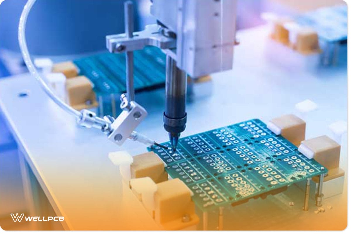
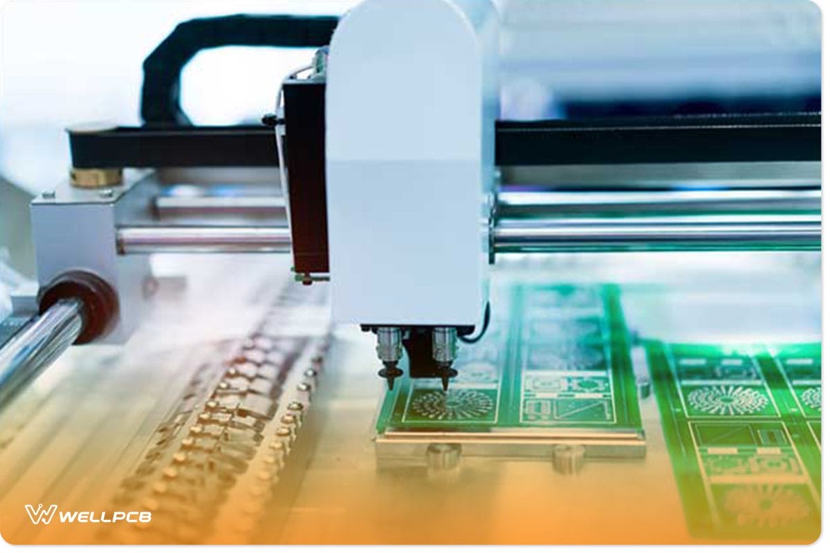
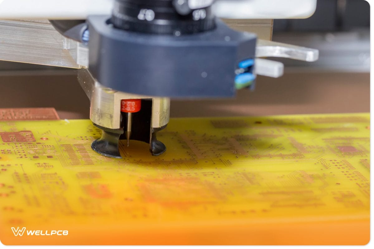
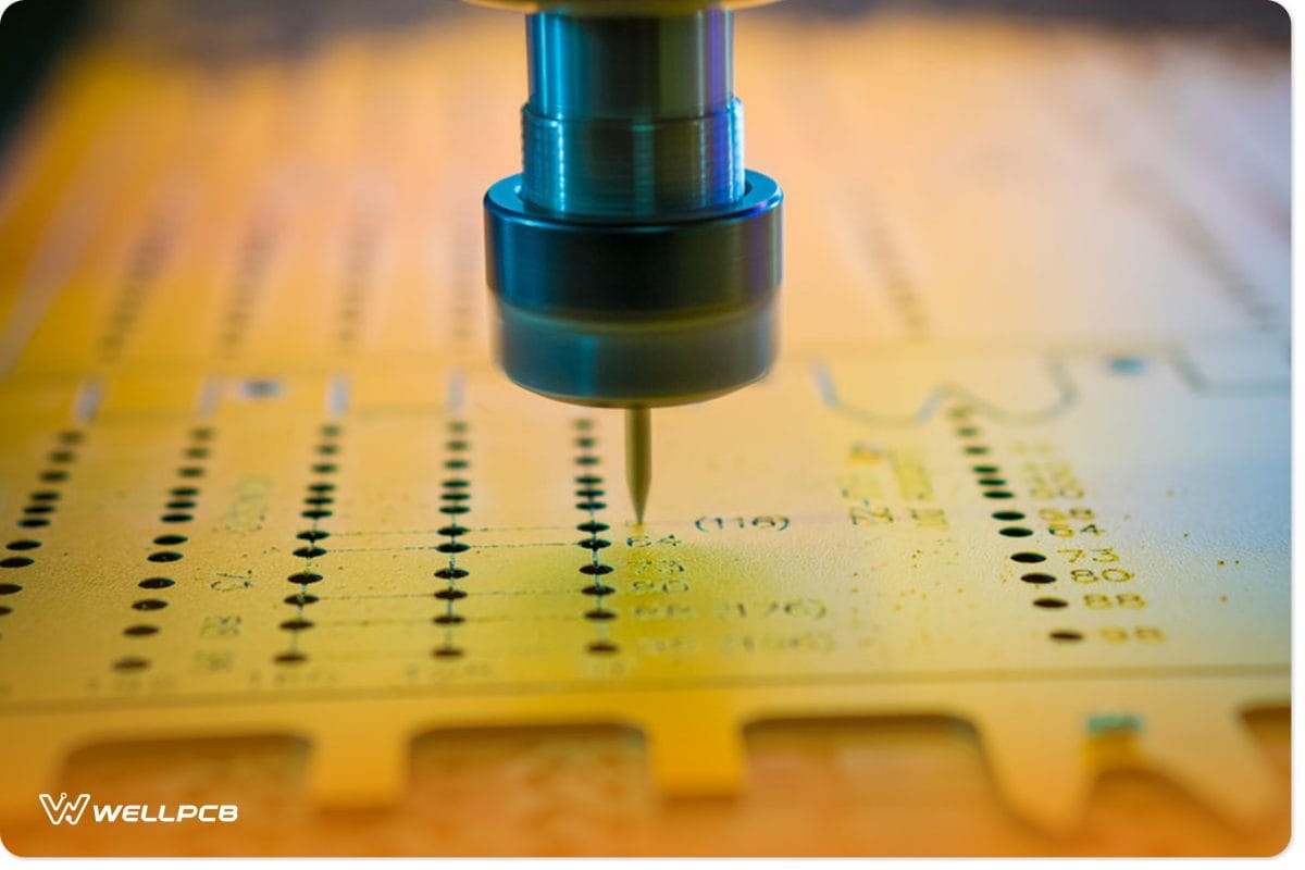
Important Keys in the HDI PCB Manufacturing Process
Aperture
One of the key parameters considered in the HDI PCB fabrication process is the aperture ratio. We must consider this ratio while designing the through and blind holes. Typically, the through-hole aperture is about 0.15mm when we use the old-style mechanical driller, and the ratio between the PCB board thickness and the aperture ratio to be at least 8:1. Nevertheless, when we use the laser driller, we recommend setting the laser hole aperture between 3 to 6 mm with an aperture ratio of 1:1 maximum.
Stack
Various factors typically affect the PCB boards during the stacking-up process, such as temperature and pressure. If the output boards from the stacking up process are not symmetric, meaning that the stress is unequally distributed on the board, a warpage will appear on one side, reducing board yield. As a result, the designer must consider the nonsymmetric stacking process design and the unequal distribution of the holes.
Process flow
We can find a lot of similarities regarding the process flow between HDI PCBs and ordinary PCBs. For instance, the process flow of an HDI PCB with six layers and two stacks is the same as the ordinary PCBs except for the drilling holes sequence. In the laser drilling process, we form the blind holes on the PCB HDI boards in high temperatures to burn the hole walls. For HDI PCB with two layers, we plate and fill the blind holes professionally, which makes the process expensive.
How to Choose the Right Material for Your HDI PCBs
The thinner materials we use in PCBs are the final product, as the materials can have a crucial factor. We can handle various materials in HDI PCB manufacturing based on the required final specifications of the product.
The necessary materials we use can be FR4, metal, and fiberglass, each of which depends on the type of product we want to make. You can select between ENIG, HASL, immersion tin, immersion silver, and gold for the HDI PCB surface finishing. We recommend ENIG because of its smoothness and flexible solderability.
What to Look For in Your HDI PCB Manufacturer
Choosing an HDI PCB manufacturer who can satisfy all your needs for building complex boards with high quality is essential. Building HDI PCB is a complex process; always look for a manufacturer with high multilayer technologies who commit themselves to providing high-quality products.
WellPCB provides a competitive advantage in manufacturing HDI PCBs. We offer fast and reliable quotes for your HDI PCBs quickly. As an experienced HDI PCB manufacturer with a long-standing reputation, we provide innovative suggestions starting from the design phase and reaching the final step of the process. In WellPCB, our engineering team is committed to delivering outstanding final products with high-quality PCBs having minimal defects. Please find out more about our PCB manufacturing services.
Global HDI PCBs Market Forecast
PCB manufacturers have devoted significant effort to HDI PCB for several years, which has a market value of $9,500 million reported in 2017. Experts expect it to reach 22,000 million by 2025, with a CAGR of 11%.
With the advent of smartphones and highly compact feature mobile media equipment, semiconductor devices continue to increase pin counts while shrinking in form. By the production year 2020, the number of high-speed I/O terminal pinouts would be over 4,000 pin-outs per flip-chip, thus requiring ultrafine pitch in the array area. However, most Chinese PCB suppliers will provide a packaging roadmap defined by ITRI. Contact the freight forwarder yourself.
These pin-out numbers will furthermore increase as the IC trend continues to follow Moore’s law. Considering such advancement in pitch size requirement, such chips’ packaging would be a challenge in terms of cost and product performance.
The most available packaging process technology in the market now depends on the HDI process, where the minimum line width/space of 100um is guaranteed for a stable manufacturing yield.
Conclusion
The most common practice of increasing the interconnection density of substrate or PCB is to increase the number of metal layers and control the total thickness of both dielectric material and metallization to obtain a smaller size for the final products. HDI PCB is the best choice for complex circuits that we need to implement in small dimensions PCBs.