Contents
- 1 What is the PCB annular ring?
- 2 The structure of the PCB annular ring
- 3 The importance of PCB annular ring
- 4 How to Calculate PCB Annular Ring?
- 5 What is the difference between a PCB annular ring and a through-hole?
- 6 Outer annular ring (OAR) and inner annular ring (IAR)
- 7 What is the teardrop annular ring?
- 8 Common problems of PCB annular ring
- 9 The annulus draws rupture probability
- 10 Skills of PCB annular ring size adjustment
- 11 Summary
What is the PCB annular ring?
An annular ring is an area of the copper pad that sits around a finished and drilled hole. The dead point here is the through-hole copper plating.
In all around this via, there needs to be sufficient copper. Enough copper enables the formation of reliable connections between the via and the copper traces.
Such is common, especially in multilayer PCBs.
Therefore, the primary purpose of annular rings is to establish excellent connections, especially in multilayer PCBs.
In other words, annular rings serve as anchors for the printed circuit board. The minimum diameter of annular rings depends on the capabilities of a PCB assembler.
Hole diameter varies according to nature and whether electroplating. Small circles do put via at risk. Small rings result in what’s known as annular breakouts.
The structure of the PCB annular ring
In mathematics, an annulus is a ring-shaped object. It’s a region that has a surrounding of two concentric circles.
The same is true when it comes to printed circuit boards. Equivalently, an annular ring is a difference that’s between two concentric circles or disks.
In adjectival forms, it’s an annular, the same way as an annular eclipse.
On printed circuit boards, annular rings are mostly circular in structure. It is important to note that the greater the annular ring’s withering, the better the copper connection around the drill hole.
If you want to avoid the chances of breakouts, you have to increase the annular ring’s size.

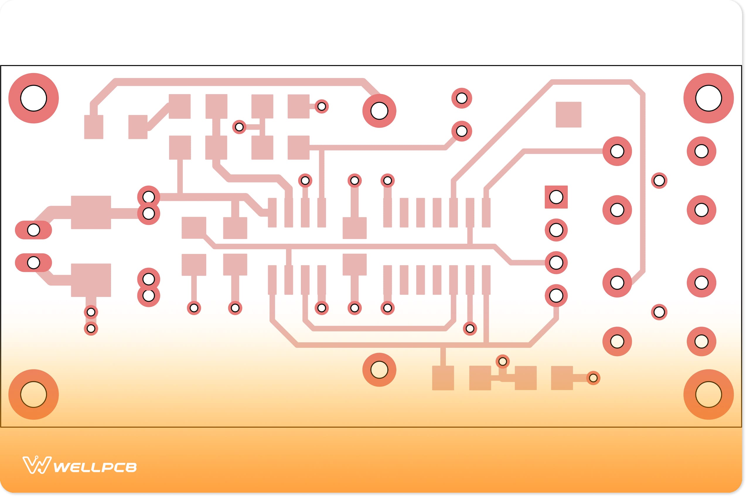
(PCBs depicting the circular structure of annular rings)
The importance of PCB annular ring
PCB annular rings are essential on a printed circuit because they give room for reliable electrical connections on a circuit board. Without annular rings, there won’t be the desired electrical connections on a circuit board.
On a printed circuit board, issues to do with annular rings can be problematic and may heavily affect trace continuity.
Additionally, it may negatively affect the functionality of the entire board.
Unfortunately, some designers don’t take into serious consideration the importance of annular rings. Some design PCBs with ugly-shaped annular rings.
Doing so is a big problem that may affect matters to do with trace continuity. When drilling annular rings, accuracy is essential important whereby drilling shouldn’t be off the mark.
If such is the case, then there will be annular ring tangency. Annular ring tangency is a problem that negatively impacts the functionality of a circuit board.
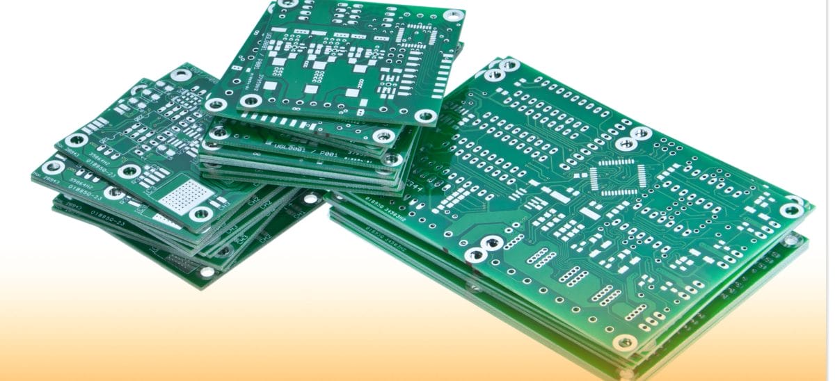
(PCBs annular rings and other electrical components)
How to Calculate PCB Annular Ring?
Determine the type according to the needs.
PCBs find a lot of use in many applications based on their high boiling points and electrical insulating properties.
They find heavy use in heat transfer, electrical, and hydraulic equipment. Lately, you can find PCBs in home appliances, military, and medical equipment.
When calculating the PCB annular ring, you need to factor in where it will find its use. The type of the annular ring depends on the needs of your PCB.
If your printed circuit board requires special requirements, then it may require high-quality PCB annular rings. The Institute of Printed Circuit Boards lists three essential classes of PCBs.
There are Class 1, 2, and 3 PCB products; level 3 ones find heavy applicability instead of Class 1 and Class 2 products.
For this reason, Class 3 annular ring requirements are slightly different. Their pad sizes need to be more significant enough to accommodate via’s diameter.
Know about the Design criteria of PCB annular ring
Without the right design criteria for PCB annular rings, you may end up with a board with poor functionality.
It would help if you got everything right so that your equipment functions as desired.
Theoretically, the best annular is achievable by drilling correctly at the center of the via pad. In a real sense, drilling accuracy depends on the equipment that a manufacturer uses.
Printed circuit board manufacturers have specific tolerances for designing PCB annular rings. Mostly, it’s about five miles.
Ideally, designers prefer locating annular rings at the dead center of the board. The reason for this is to ensure excellent connectivity between the layers and the vias.
During the design stage, it’s essential to have a proper setting of the annular ring.
For dense designs, then it’s vital to have smaller annular ring sizes. The reason for this is that via or the pad will consume small spaces.
Use the Calculation formula.
The calculation formula of PCB annular rings isn’t as complicated as you may think. Unfortunately, though, many people aren’t aware of arriving at such calculations.
For reasons of creating via, it means that the drilled hole requires a copper surrounding. The ring of copper is the via size or the outer diameter.
According to IPC-2221A standards, the calculation of the minimum PCB annular ring size is as follows:
Minimum Annular Ring = (Min Ringer Border) * 2 + (Tolerance) + (Hole Size)
The annular PCB ring is (diameter of the pad – the hole) /2. Assume that you have a pad diameter of 20 mils and a hole diameter of 10 mils.
For this reason, the annular ring width will be 20 – 10 = 5 mils.
If you know that you have a particular pad with an annular ring of 8 mils, then the pad diameter is 8*2. That will be equal to 16 miles.
As you can see, the calculation formula of PCB annular rings isn’t a complicated process.
Minimum annular ring
You need to pay attention to the minimum ring width. It is important to note that there’s a minimum annular ring on the inner and outer layers of a PCB.
Most designers agree on a minimum annular ring of 0.1mm on the inner layers of a PCB.
Also, most PCB designers agree on 0.05mm as the minimum annular ring on the outer layer.
If you want to achieve the best and most desirable minimum annular rings, then you’ll need to consider a few things.
But the most important thing is to ensure that you work with a designer who values Design for Manufacturability (DFM).
With DFM, you’ll acquire PCBs with the minimum size of the annular ring.
What is the smallest annular ring?
Sometimes, based on the nearby elements’ tight spacing, designers choose to make small PCB annular rings.
It is important to note that small annular rings increase the chances of drilled vias being close to the annular rings’ edges.
In worst cases, the drilled via may break out of the annular ring. Such may amount to a broken trace connection.
Much worse, it may result in a fragile relationship, affecting the functionality of the board. The smallest annular ring is -1mil.
Unfortunately, that’s not ideal because it increases the chance of a breakthrough.
How to calculate the smallest annular ring
As noted earlier, estimating the size of the annular ring isn’t a hard thing as such. Again, the smaller the annular ring, the better. Small annular rings are excellent when it comes to cost savings.
Like the maximum annular ring calculation, the same is almost precisely calculating the smallest annular ring.
To calculate the smallest annular ring, you need to take the copper dimension and subtract it from the drill diameter. The figure should be divided by two.
A majority of PCB designers agree that the smallest annular ring needs to be 0.050mm.
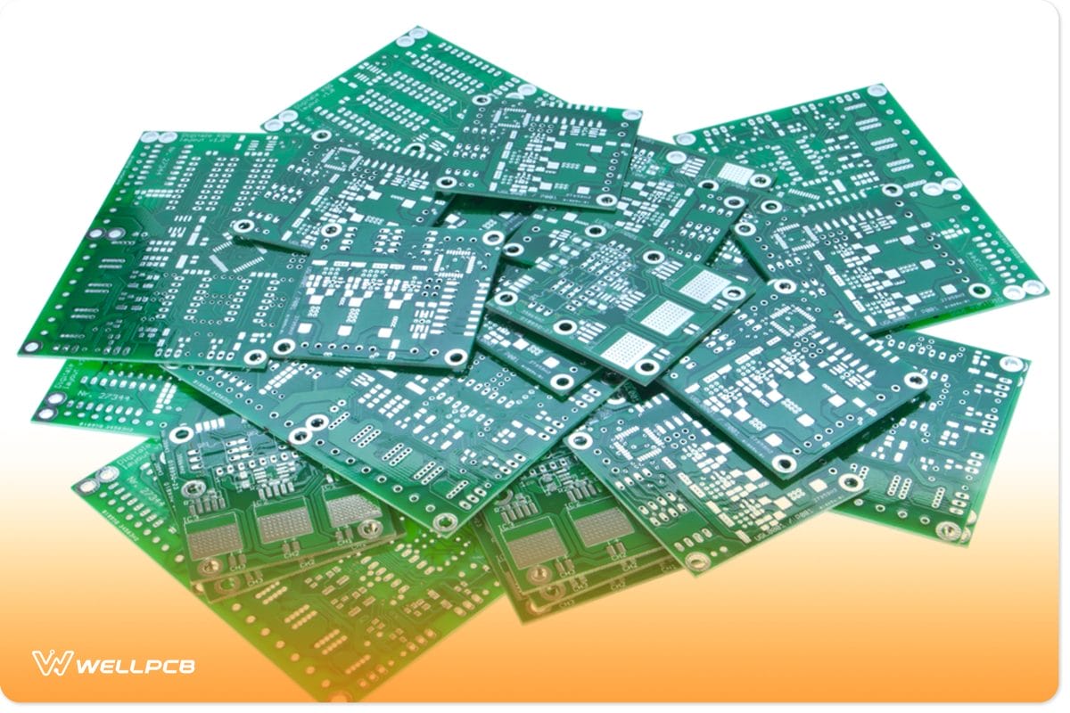
(PCBs with the same annular ring size width)
What is the difference between a PCB annular ring and a through-hole?
There’s a difference between a PCB annular ring and a through-hole worth noting. The area between the copper pad and the edge of the drilled via is an annular ring.
As stated earlier, if the width of the annular ring is large, then the better. Doing so can provide connections for drilled vias.
On specific printed circuit boards, annular rings are almost of the same size.
When it comes to PCBs, you’ll often hear of the term through-hole. Also spelled as “thru-hole,” such refers to a mounting scheme applicable for electronic components.
It involves the use of leads on elements inserted into holes drilled in the PCB. Of importance to note is that through-hole is one of the oldest technologies.
However, there are valid reasons for using it. For instance, a through-hole is ideal for hobbyists. It comes with a little fuss and a few errors of accidentally bringing about bridges.

(A machine drilling PCB annular rings)
Outer annular ring (OAR) and inner annular ring (IAR)
An Outer Annular Ring (OAR) is different from the Inner Annular Ring (IAR), as explained below. Both are different in terms of terminologies and their calculation.
What makes the outer annular ring
An outer annular ring consists of a copper pad. The copper pad is the essential material that you’ll find in an outer annular ring.
Calculating the Outer Annular Ring is an easy process. The outer annular ring is 1 / 2 (The outer pad diameter ). Here is a clear example of how to calculate the outer annular ring:
OAR = (Copper pad diameter – TOOL SIZE)/2. That’s how to achieve such measurements. The TOOLSIZE = END SIZE + 0.10mm for PTH holes + 0.00mm for the entire NPTH holes.
What is an inner annular ring?
The Inner Annular Ring (IAR) is the area that lies between the solder hole and the outer layer rim of the solder pad.
It’s as simple as that. Much better; it’s not a difficult process calculating the inner annular ring of a PCB. It’s all explained below:
The Inner Annular Ring is 1 /2 (Inner layer pad diameter – ). To calculate the inner annular ring, you need to take the copper pad diameter minus the TOOLSIZE.
After that, you need to divide the figure that you get by 2. The TOOLSIZE = END SIZE + 0.10mm for the entire PTH holes + 0.00mm for the entire NPTH holes.
Assume that you want to calculate the IAR on a copper pad of 0.60mm with a finished hole consisting of a diameter of 0.25mm. Therefore, the IAR will be as follows:
0.60mm – (0.25mm + 0.10mm) /2. This will be equal to 0.60mm – 035mm / 2 = 0.250 mm/2. The result is 0.125mm.

(PCBs inner and outer annular rings)
What is the teardrop annular ring?
When it comes to the manufacture of PCBs, you may come across the term teardrop. The name comes based on its shape.
Teardrops mostly occur during the drilling process. During drilling, possibilities of drill bit misalignments are common. Here, a drill bit may remove a lot of copper from the junctions of a PCB.
Such may bring about broken trace connections or a thin connection. But of importance to note is that teardrops play essential roles in PCBs.
A majority of designers use them to prevent micro cracks. Microcracks mostly occur at the connection of the pad and the track.
However, the primary purpose of teardrops is to ensure integrity during PCB production.
Such is true, especially in cases where the drill bit gets misaligned during drilling.
There are other reasons why PCB designers use teardrops. Some of the most important reasons include the following:
- It minimizes the risk of cracking.
- They significantly improve resistance to the thermal shock of equipment.
- It minimizes thermal and mechanical stress in places where trace joins the pad.
- It helps in enlarging the PCB maker tolerance of the drill to pad. Such makes the production of a circuit board more comfortable.
- It dramatically reduces the chances of cracking.
- Teardrops also make circuit boards more mechanically robust.
Common problems of PCB annular ring
Undesired annular ring
Undesired annular rings are common PCB problems. If the pad size tends to be small, it may fail.
The reason for this is that the drill hole will consume a lot of space on the pads. For designers to avoid such, prototyping is necessary.
Prototyping ensures the avoidance of undesired annular rings before full production. With prototypes, it’s possible to detect errors early before mass production.
Tangency
Annular PCB ring tangency is another common problem that faces PCB designers. The moment a drill misses the desired mark, the resulting hole edges towards the pad’s size.
The moment the spot gets to touch the edge of the place, it brings about an annular ring tangency.
If the drilling gets to deviate further, then it’s dangerous. Such brings about instances of breakouts. If you are to avoid tangencies, you have to ensure that the drilling is perfect.
Your drill should hit the mark. The accuracy of the drilling should be on point.
Breakout
Breakouts are also common problems of annular PCB rings. Annular breakouts happen the moment the drilled via doesn’t get the desired encircling by the pad.
Mostly, breakouts occur when the lamination process causes parts of a PCB to move away from where they must sit.
Do you want to avoid cases of flights? If so, you need to ensure that the width of the annular ring is ideal.
As mentioned earlier, the annular ring width is the pad’s diameter – the diameter of the hole / 2.

(Annular ring breakout on a PCB)
The annulus draws rupture probability
What is the rupture of the annular ring (causes)
Several causes may cause annular rings on a PCB rupture. In most cases, it’s due to the aging of a circuit board.
Boards that are old or perform for too long are prone to annular ring rupture. With age, rest assured of a component rupture.
Additionally, annular ring de-wetting is another reason for the break.
Contamination of the holes during the manufacturing process is another reason for annular ring rupture. There are other causes known for bringing about the fracture of the annular rings.
Excessive mechanical stress is known for bringing about the crack of the annular rings. However, all is not lost, as there are ways of avoiding instances of the break in the annular rings.
How can we avoid
There are several ways to ensure that you avoid cases of rupture of the annular ring. First of all, you need to ensure that the type of material you use is of the highest quality.
Also, you need to ensure that you work with qualified manufacturers. If you source your PCBs from experienced manufacturers, rest assured of no chances of annular ring rapture.
You may also have to replace your PCBs, especially if they are old. Make sure that you don’t subject your PCBs to excessive mechanical stress.
To be on the safe side, ensure that there is no hole contamination. Make sure that the manufacturing process follows all the procedures to avoid such cases.
Skills of PCB annular ring size adjustment
If your annular rings’ sizes are off, then it could mean problems in your circuit board. Annular rings that are not of the desired size will not function as intended.
Issues with the size of the ring occur if the drilling isn’t accurate. However, changing PCB annular ring sizes requires some special skills.
Such is easily possible, especially if you have some tools.
The best tools are those that are available from Cadence and are excellent for designing PCBs and analysis.
If you use the OrCAD PCB designer, you’ll be able to get the desired annular ring sizes.
All that you have to do is key in your desired pad and the length of the hole. You have to do this during the PCB layout design.
Summary
The toroid is very important on the PCB. They act as interconnect nodes, operating between different layers of the PCB.
Without annular rings, PCBs won’t function as intended. Unfortunately, many PCB designers don’t get it right when it comes to annular rings.
Many fail to get the correct width, while others end up with annular ring rupture challenges.
Do you require high-quality PCBs with the best annular rings? If so, look no further than WellPCB. We manufacture some of the best PCBs with the designed annular ring width. Our circuits rarely suffer from tangency and breakouts. For the best PCBs, source them from us. With us, we can organize exchanges so that we learn matters to do with PCB together.