Contents
- 1 In rapid Designing, how can to solve the problem of signal integrity?
- 2 In rapid Designing PCBs, the blank area of the signal layer can be applied to the copper, and how to allocate the deposited copper on the ground and the power?
- 3 In rapid Designing PCBs, How do we Consider the Impedance Matching Problem?
- 4 What is FR-4 in PCB Fabrication?
- 5 In 2G High-frequency Designing PCBs, Line, Typesetting, what Aspects Should Focus on?
In rapid Designing, how can to solve the problem of signal integrity?

In rapid Designing PCBs, the blank area of the signal layer can be applied to the copper, and how to allocate the deposited copper on the ground and the power?

In general, most copper in the blank area is grounded, just at the high-speed signal line next to deposited copper. We should pay attention to the distance between the copper and the signal line because the deposited copper will reduce the line’s characteristic impedance. Also, note that it does not affect the layer’s characteristic impedance, such as the dual stripline structure.
In rapid Designing PCBs, How do we Consider the Impedance Matching Problem?

Impedance matching is one of the key elements of design, and the impedance value has a positive relationship with the route. For example, microstrip or stripline/double stripline. The distance between the reference layer (power layer or stratum), the line width, the material, and so on will affect the line’s characteristic impedance, that is, to determine the impedance value after wiring. The only way to solve the problem is to avoid the occurrence of impedance discontinuity.
What is FR-4 in PCB Fabrication?
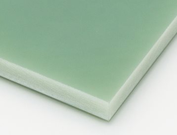
This is a fiberglass composite meant to make the PCB flame-resistant or flame-retardant (FR). Other than FR-4 substrate laminate, there are other options, but they do not have a good strength-to-weight ratio as the FR-4. This has made FR-4 become a well-accepted standard.

In 2G High-frequency Designing PCBs, Line, Typesetting, what Aspects Should Focus on?
2G or more high-frequency PCB RF circuit designs are not in the design of high-speed digital circuits.RF circuit layout and routing should be considered together with the schematic because they will cause a distribution effect. Moreover, the RF PCB design of some passive components is defined by parameterization and special-shaped copper foil. Therefore, it is required that the EDA tool can provide a parameterized device and edit special shape copper foil. In general, RF PCB design requires a dedicated RF circuit analysis tool.


