On PCB Etching for Design, The copper layers get central attention due to their developments in a printed circuit board by keeping other layers updated for supporting or protecting the circuit or used for simplifying the assembly process.
The PCB designers at the starting phase are merely focused on getting connected from point A to point B by reducing as many problems as possible.

However, by spending time and expertise, the primary attention of PCB designers is to improve the following functions;
- Refinement of the PCB
- Dedicating resources for artistry work
- Space utilization
- Enhancing the overall performance of the PCB designs
Contents
- 1 PCB Etching for Design–Low-Cost Boards
- 2 PCB Etching for Design–Homemade PCBs
- 3 Professionally developed Boards
- 4 Steps in the Etching of PCB Boards
- 4.1 1. Even the application of Photoresist to the Copper made Clad Board
- 4.2 2. Using Powerful UV light exposing undercover portions of the Board
- 4.3 3. Submerging the solution of the entire Board by removing the hardened photoresist
- 4.4 4. Using a copper etchant to remove undesired Copper from the Board
- 4.5 5. Drilling the holes in the PCB
PCB Etching for Design–Low-Cost Boards
The low-cost boards describe PCB designs at the expense of the highest quality and speed.
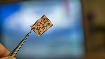
PCB Etching for Design–Homemade PCBs
Homemade PCBs are ubiquitous among their users due to their turnaround time.

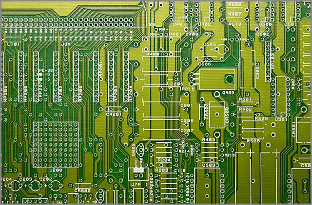
Professionally developed Boards
The professionally developed boards are based on the following points;
- These boards are developed using the latest technologies and advanced methods that enhance the capabilities and tolerance of these boards
2. Professional boards are developed by using etching technologies that are much better than traditional technologies for better equipment and expertise
3. These boards ensure a difference between the professional boards and amateurs because their tolerance level is tightened due to huge influential factors of expertise
4. These boards are ideally suited for luxury homes due to the difference between acceptable and great board houses

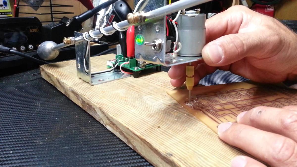
Steps in the Etching of PCB Boards
Different steps involved in the etching of PCB boards
1. Even the application of Photoresist to the Copper made Clad Board
PCB boards’ photoresist is UV sensitive, ensuring hardness when exposed to associated environments. It is covered by a negative of the copper layer image placed on the PCB.
2. Using Powerful UV light exposing undercover portions of the Board
The powerful UV light makes the Board stiff and sustainable to the environmental conditions.
The technology used in the development of this Board is similar to the technology used in creating semiconductors with features measured in the tens of nanometers.
Therefore, the method used in this PCB etching can show excellent features.
3. Submerging the solution of the entire Board by removing the hardened photoresist
4. Using a copper etchant to remove undesired Copper from the Board
It highlights an exciting challenge in the etching process which is desirable in anisotropic etching. Using the copper etchant, it is moved downward, and the edges of the protected Copper are unprotected and exposed effectively.
On the other hand, thinner traces are associated with smaller ratios of the protected top and revealed side layers.
5. Drilling the holes in the PCB
Holes are successfully drilled into the PCB for all different uses, and electroless Copper is deposited once the spots are successfully trained in the PCB.
The electroless Copper is used explicitly to build up Copper within the hole in the walls and create the value for the electrical connection through the Board.
It shows how PCB is made up and designed as designers need not have years of work experience in manufacturing and assembling such PCBs that are solid in quality by understanding the way of doing things to ensure more significant insights into both the how and why good PCBs are designed.
If you are a starter or experienced manufacturer of PCB, you have a bright future in China because its manufacturing is getting popular in this country.
Manufacturing is associated with the most promising features or functions that the manufacturers can provide to their customers according to their expectations.
Customers can select shipping options from China according to their convenience after selecting their appropriate shipping agent. The most effective PCB manufacturing in China is that manufacturing is cost-effective and cheaper than its competitors.
The customers are advised to review their PCB designs by visiting the website of WellPCB, which is a popular manufacturer of PCB in China.
Customers can order their selected PCB designs or call the customized designs according to their preferences and requirements.
You can conveniently place your orders by visiting wellpcb.com, enjoy excellent options for the plans of the PCBs, and demand the development of customized PCB assembly addressing your requirements.
The company offers tremendous resources to its customers to test the quality and functionality of the prepared PCBs to ensure the products work well at the customers’ end.