Contents
- 1 Choose Components During the Design Phase
- 2 Think About Component Footprint Decisions
- 3 Use Good Grounding Practices
- 4 Separate Non-lead-free from Lead-free Components
- 5 Assign Virtual Parts Footprints
- 6 Ensure You Have Complete BOM Data
- 7 Sort Reference Designators
- 8 Check Spare Gates
- 9 We Need to Fill the Pads
- 10 One Pad For One Connection
- 11 Consider the Component Package Choice
- 12 The Land Design Matches the Setup of Leads on a Component
- 13 Address Your Component Delivery
- 14 PCB on Both its Top and Bottom Sides
- 15 Summary
Choose Components During the Design Phase
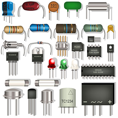
The design phase of your PCB should be the stage where you choose your PCB components because your design will determine the appropriate parts to select from the market. In like manner, the ingredients available in the market will also influence your PCB design.
Therefore, you should choose a design that captures the height and width. Other attributes of the component you want to use. These components include resistors, capacitors, transistors, and other necessary components.
You may choose to create a new design requirement—compact design, power-oriented design, or affordable design—or you can choose from your previous designs. Following this tip will hint you at other parts of the design phase, including your component choice.

Think About Component Footprint Decisions
As a PCB designer, you must select PCB component footprints and land patterns that provide firm roots for the PCB components. You must ensure you settle for a print that matches the land design. As the datasheet shows, using the numeric keys to make a strategy is perfect.
A PCB designer who does not comply with the datasheet is highly likely to get an incorrect component footprint, which can lead to many design errors.

Use Good Grounding Practices
The ground planes are essential parts of the PCB with components that should possess many bypass capacitors. After appropriate by an integrated circuit (IC) pin fixed capacitor, they will allow easy circuits and create room for fast performance.
Wne cannot ignore these capacitors, so you should watch out for the size and frequencies. Ensure you prioritize good grounding practices during your PCB design process.

Separate Non-lead-free from Lead-free Components
When choosing a PCB component, it is essential to separate defined lead-free parts from the undefined ones to ensure a lead-free arrangement. If not specified, it is crucial to label all ingredients as lead-free. But note that this is only right when there is no alternative for the leaded solder in a particular project.
A designer should not make this modification without the customer’s awareness because there is a variation between the lead-free and the non-lead-free. For instance, the Government platform motherboard must use lead solder design.

Assign Virtual Parts Footprints
The virtual parts contain ground and power signals. Wne need to consider these virtual parts during the PCB component schematic construction process. We cannot dispute the importance of the virtual parts during the process of designing PCB components.
Get a better understanding of your PCB assembly‘s virtual parts when you keep in sync with the bill of materials (BOM) created by providing a list of virtual elements.
The best thing to do is attach the PCB virtual parts to footprints and assign functions to them in accordance with the BOM to give the PCB an exotic design.

Ensure You Have Complete BOM Data
Another thing to give absolute attention to is the Bill of Materials data. The BOM data must be complete. You can follow the BOM report for informationAfter that, review and fill in the manufacturer’s information on every part before you advance to the PCB design stage.
A complete BOM can help PCB suppliers work faster and solve some problems as soon as possible.

Sort Reference Designators
The reference mark (RD) is part of the BOM, which specifies each PCB component’s usage and how to find it.
Sorting the reference indicator is another thing because it helps to arrange the contents of the BOM. To effectively work with your reference designators, you must endeavor to number them for a comfortable mechanism and review.
It Means that your reference number must correspond to your BOM data and keep in mind before PCB design.


Check Spare Gates
To ensure that the PCB system works effectively, you must check out for every additional barrier. The other door is essential because you want to connect the input to the signal to act as a part that won’t float.
To promote PCB independent functions, every spare gate in the drawing helps to understand and run the board for the team members. The component symbols made for PCB layout and finally printed over the PCB board are helpful during PCB assembly must be correctly positioned, especially when connecting to an unwired input.

We Need to Fill the Pads
Via-in-pads are holes reserved to help provide a good fit for the PCB components and ensure perfect connectivity among the elements.
The primary function of PCB Via is to ensure that power is available between all connections in the PCB. They are essential to prevent any interloping that could lead to severe destruction.
Another Via role is to ensure that the solder does not float when assembling the entire assembly, thereby enabling reliable soldering.

One Pad For One Connection
The composition of the PCB components must follow the one-pad-for-one-connection rule for proper alignment during the assembling process. If there is a mix of components on the pad, such as capacitors and resistors, you must recreate another pad.
Please always avoid creating pads that are not the size of other pads. This facilitates imbalances in the solder joint.
Peradventure, there would be contact between the planes; do not forget to clarify the pads.

Consider the Component Package Choice
It would help if you chose the PCB components package to supplement your aesthetic design and intrigue your customers. This is another essential tip that some PCB designers fail to follow, which works against them.
Choose a component package that can add a touch of perfection to your design, and it will speak well about your proficiency as a PCB designer.

The Land Design Matches the Setup of Leads on a Component
It would help if you used a well-framed land design pattern to match the setup of leads on each PCB component. It automatically gives each PCB component a structure that provides room for the placement of other properties needed to complete the PCB setup.
For once, PCB designers should not ignore the importance of a land design that corresponds with the setup of leads on the component.

Address Your Component Delivery
It is unrelated to the designing section, But this is another technique for making a PCB with perfectly formed components. This focuses on the component’s delivery aspects. According to the BOM, the PCB components should be delivered in parts to ensure the appropriate organization of all the kits.
For example, manufacturers may accidentally call unnamed materials on the BOM. Let’s say an extra component of 20% addition of 0201 1k ohm resistors. You should not, for any reason, mix the ingredients to avoid unnecessary hiccups. Instead, package the extra parts in a separate bag with appropriate labeling.
It is essential to agree with your manufacturer on the best means of conveying the components. This will prevent some of the usual problems faced during delivery.

PCB on Both its Top and Bottom Sides
You must consider the house that the PCB will have. It involves paying attention to the PCB height, including the top and bottom sides, to derive an adequate PCB at the end. It also encompasses understanding the PCB’s perimeter and how to structure it for easy mobility and portability.
Also, some PCB components have height restrictions, so you have to ensure that your component choices are feasible.

Summary
The clues above are essential for all PCB designers to consider when deriving their desired PCBs with incredible components. Following these tips will give you an elegant PCB and a PCB that will serve your needs or the needs of your customers.
Regarding the selection of PCB components, I believe you have a lot of knowledge. If you like to read more, you can contact WellPCB. Wne have 10 years of PCB production experience, help you solve problems, and provide quality services. What are you waiting for? Please circuit board shopping, various things might get you confused. Whether you are going for a single-sided PCB, a double-sided PCB, or any other type of PCB, You can contact us!