PCB Via is essential in the case of a multi-layer PCB. PCB is a multi-floor construction with various passages and links between two or more adjacent floors. As complex as it sounds, designing and implementing a multi-layer PCB is a highly complex process. Without vias, the construction of a reliable and high-quality multi-layered PCB is nearly impossible.
So, this article is all about what I learned about PCB Vias. Let’s get started.
Contents
1. PCB Via Size Requirements
PCB vias help make more compressed designs by routing traces via the PCB rather than on the surface. It supplies a conductive way for an electrical signal to go from one circuit layer to one more. This conductive way is a plated hole wall. Anyways, you will have various options for the ultimate look of the PCB vias.
1.1 PCB via Size
First, you need to ask your manufacturer for the most miniature annular ring and least drill size they will use in the PCB vias manufacturing process. The usual mechanical exercise will have diameter sizes not more miniature than 12 miles without regular rupture. Hence, your manufacturer may raise the expenses to compensate for ruptured drills.
You will see that annular rings will not have less than six miles in diameter for standard processing. Therefore, the minimum size you can get will have a 24-mil diameter pad and a 12-mil diameter hole.
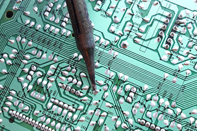
Figure 1 demonstrates a surface mount tech (SMT) micro-chip placed on a PCB via.
1.2 Standard PCB via Sizes
You would know that in simplest terms, vias are holes. So, the manufacturers can create all of the standard sizes of a drill. However, keep in mind that the development process will be proficient if the PCB has vias of the same size.
If PCB vias have the same size, it will also save a substantial amount of your time and the production cost. Can you guess why? It is because it will make the drilling process simpler. You can drill vias having a minimum size of 0.15mm and a 0.3mm solder pad. And, the maximum drill size can be as large as you may like.
On the other hand, different PCB via sizes may need a manual drill process to raise production expenses. In many PCBs, you will find that vias with a 1mm solder pad and 0.6mm hole size are most commonly found. However, you can make PCB vias smaller than 0.15mm by using a laser drill.
In this section, I have discussed the different possible sizes of the PCB vias. And, in the next section, I will tell you about various kinds of PCB vias.
2. PCB Via Types
2.1 Plating Through Hole
PCB vias can be categorized into three different kinds, i.e., blind via, buried via, and through-hole vias. However, I will discuss through-hole vias in this subsection, and the next ones will include the other two types.
Every type is categorized depending upon its position on the circuit board. Through-hole vias connect the bottom and top layer of the circuit board by moving via the inner layers.
You will find that these kinds of vias are mostly the least expensive. Further, they are also simpler to develop a style as they only require a plated through-hole. And a plated through-hole can be either laser cut or a driller.
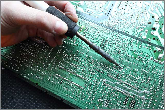
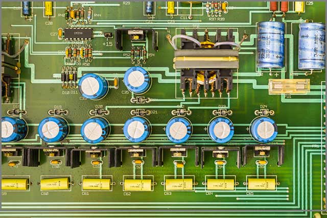
Figure 2 shows electronic components soldered on the plated through holes.
2.2 Blind Via
Coming to the blind vias, they are mechanically drilled. However, they break at a point before going through the whole printed circuit board. You will see that blind vias get bored from the bottom or top layer.
Blind vias, being mechanically drilled, can connect an outer layer to a nearby layer. Also, for some cases, an additional layer underneath and careful planning are needed to achieve better results.
A blind via can only be seen on one side of the PCB compared with a through-hole via. Hence, the plating solution cannot flow via the whole hole, and thus this makes the plating part complex.
Unlike a through via, a blind via is only open at one end, so the plating solution cannot flow through the hole all the time. That complicates the plating process. Moreover, blind PCB vias usually make a connection between ground rails, power, and internal layers.
2.3 Buried Via PCB
Coming to the buried vias, they are also mechanically drilled. They are utilized to make a connection between inner layer assemblies only. Initially, they are bored as through vias from top to bottom of an internal layer structure which would be laminated. For example, from L2-L4 of a 5-layer printed circuit board. After that, it is plated and prepared for the last lamination.
In other words, we can say that buried vias are embedded into the printed circuit board. It is because it makes a connection between two internal layers of the PCB. In this chapter, we have introduced you to the types of PCB vias. In the next section, we will give you the tips to select the best PCB via type.
3. Tips For Choosing The Best Via Option
In the previous section, we told you about the three main types of PCB vias. Now you have to wonder what type you should use and when. This section is dedicated to giving you tips for selecting the best via kind or option.
First of all, you should take into account the following main points before implementing any PCB via:
- Consider usage.
- Take into account the complexity.
- Also, consider how the selected PCB will affect the turnaround time of your board’s manufacturing.
- Lastly, I also consider the expenses it will be getting you into.
Now, we will mention a few more tips to help you choose the best PCB via type depending upon your design.
- 1: Select the least complicated PCB via a type that can meet the requirements of your design. It will decrease your manufacturing costs and turnaround time.
- 2: Utilize non-conductive epoxy fill whenever possible. It is cheaper and mostly enough for many signal routing.
- 3: Use buried and blind vias to remove stubs while routing high definition multimedia interface (HDMI) or similar high-speed signals.
- 4: Utilize conductive fill for vias that need high power. The capability of higher thermal conductivity can be beneficial for quickly directing heat away from high power components.
- 5: Ensure that the plated hole surface is planar while using tented vias. It will make sure that components are placed at the same level. Further, it will also ensure components tombstoning.
- 6: Make it your last option to use via-in-pad and ensure that your manufacturer can dependably make them.
- 7: Go for through-vias if you are looking for the cheapest via type or option.
- 8: Discuss with your manufacturer if you are planning to use buried or blind vias. You should do it before making a board layout to know about their abilities.
Hopefully, these tips will benefit you greatly. The following section will tell you about the main difference between a PCB via and a pad.
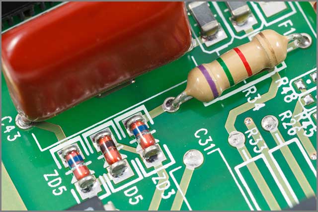
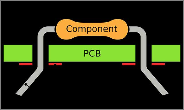
Figure 3 illustrates many different types of PCB vias located on a printed circuit board. The hand is soldering a through-hole component.
4. What Is The Difference Between A Pad And Via?
If you look at them physically, vias and pad are identical. Both of them are created using the same procedure. Further, a plated through-hole connects them, and both of them have copper rings on the bottom and top layers.
You may desire to use pads in locations where you want to solder a component lead. It would help if you did not hesitate to connect traces to the place on any layer. PCB vias are utilized when you would want to send a signal from layer to layer. They cannot be used for soldering electronic components.
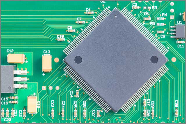
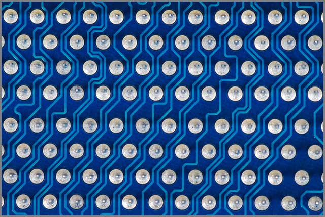
Figure 4 illustrates a pad on the PCB. We are hopeful that after reading this section, you will not confuse a PCB with a PCB pad again. In the next chapter, we will tell you about three different procedures for filling the PCB vias. Buckle up.

5. Via Tenting, Plugging, and Filling
5.1 Via Tenting
Via tenting is the procedure to make tented vias. They have a non-conductive solder mask covering them. In this case, you should not worry about filling the PCB vias. This procedure can also develop a small space with air confined in the via.
The same problem exists in tented vias as the PCB soldering process requires heating up. And, you would know that heating gas can give you a mini-explosion due to expansion. Hence, you should avoid this problem by keeping a small space in the center of the tent. This small space will allow the tented via to breathe.
Further, this would permit the via to lie close to the pad without having solder going down the hole.
5.2 Via Plugging
Generally, you will need to fill the via with a solder mask having a low-viscosity level. It will give you plugged vias. Other appropriate materials like resin utilized for laminate construction can also be used for filling the via.
The filling protects the copper, so additional surface protection is not needed. Your manufacturing costs will also go down. However, you will get no or slight thermal advantage from them when compared with conductively filled vias. And there are different fills available as many board materials grow with different ratios.
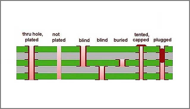
Figure 5 shows many different types of PCB vias that we have discussed until now. You can check it to clear out your concepts about separate PCB via types further.
5.3 Via Filling
Via filling is the process where you will need to fill through-hole PCBs with copper. Thus, you can also say that they are conductive PCB vias. In this procedure, your PCB manufacturer should try his best to develop an even layer of copper inside the PCB vias without forming a thick outer layer.
If you don’t utilize proper methods, you can end up with an accumulation of copper. This overabundance can put too much copper on the traces or raise the weight of PCB. Thus, you will fail to meet the specifications of your design.
Day by day, as via holes are getting smaller. It is essential that you strictly meet your design requirements. Standard via filling approach includes utilizing pure copper for filling the gap. But, this method frequently causes the development of voids where impurities can get trapped in the copper.
Furthermore, this void can also discharge gas when you heat it in the following production stages. It will develop holes that will disturb the connections among the copper layers of the PCB. However, you can avoid this issue by making an “X” patterned connections in through-hole vias. Also, you can leave a break at the top when you are filling a blind via.
The next chapter will tell you how PCB via plating uses are different from PCBs via filling.
PCB Via Plating Applications
No doubt, you will increase the capacity when you fill PCB vias with copper. But, it will also cost you more when compared with copper-plated PCB vias. Some applications may need the additional dependability but not all of them. Thus, you can also use a PCB via which only has copper plating smeared along the traces of copper.
You should always consider the voltage and heat requirements of an application where you need PCB vias. An accurately developed PCB with plated through holes can work quite well without malfunctions for low-power uses.
Figure 6 demonstrates electronic components placed on plated through holes.
In the same way, applications that need high operating power should use copper-filled vias. In the coming chapter, we will tell you about PCB via rivets and its inductance.
PCB Via Inductance Calculator
Hopefully, by now, you all will have a vivid vision of PCB vias. So, in the end, we will tell you how to calculate the inductance of any PCB via. According to Howard Johnson, this simple formula can be utilized to calculate PCBs via inductance:

Where his PCB thickness is in inches and d is PCBs via barrel length in inches.
At this point, we would also tell you about PCBs via rivets to further enhance your knowledge. And, don’t worry, they are not something complex. You can utilize them to secure terminals to a printed circuit board.
Figure 7 shows a PCB with silver studs or rivets.
Conclusion
As high-density designs evolve, the requirements for PCBs via types and handling are more complex and higher.
Because different manufacturers may have other equipment and requirements for hole handling, you need to clearly state all the requirements and check Gerber files together to ensure the accuracy of the data and parameters in the document; this can effectively avoid delaying the quotation and production.
Contact us at [email protected] if you need any further assistance or have any questions. We will contact you instantly and will clear out any confusion you may have.


