On PCB Development, The age of the Internet of Things is here, and it’s taking over virtually every facet of the digital world. Expects have described IoT as “the fourth Industrial Revolution” and “the biggest thing since the .com explosion.”
And if recent reports from Gartner count for anything, planet Earth will have at least 20 billion internet-enabled devices in PCB development by 2020.
Developers develop intelligently connected platforms for innovations like wearable devices, home automation, medical monitoring systems, intelligent cars, and futuristic cities by tapping into the technology.
IoT presents an optimistic take on connectivity between physical and digital components as the newest tech kid on the block. This article will talk about the development and future of the Internet of Things in detail. Do you want to know more about it?
Contents
- 1 IoT: Driving New Approaches to PCB Development
- 2 Fabricating PCBs For IoT: What’s Different?
- 3 PCB Development–IoT And The Future Of PCB Design
- 3.1 1. Diminishing Layouts
- 3.2 2. Better Packing Technologies
- 3.3 3. PCB Development—Encompassing Designs
- 3.4 4. PCB Development—Standardization
- 3.5 5. Collaboration with Mechanical Designers
- 3.6 6. PCB Development–New Materials
- 3.7 7. More Emphasis On Wireless Connectivity
- 3.8 8. Sharper Focus On Power Consumption
- 3.9 9. PCB Development—PCBs For The Human Body
- 3.10 10. PCB Development—A Firmer Take On Reliability
- 4 PCB Development–Conclusion
IoT: Driving New Approaches to PCB Development
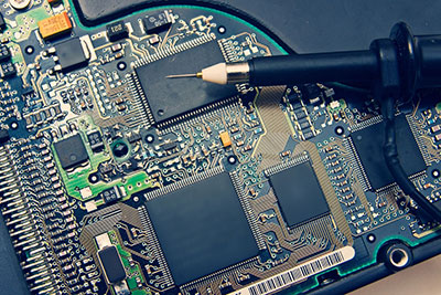
One of today’s top trends in PCB development is the increasingly prevalent use of flex, and high-density interconnect (circuit board Making. THE conventional PCB routing methods can not achieve this. With HDI) boards. Most IoT devices are meant to be used while in motion, and the use of flex PCBs simplifies wiring while providing extra resistance from harsh conditions.
Furthermore, as the board surface area decreases and routing density increases, developers turn to the fabrication of rigid PCBs. Here, the conditions apply to multilayer, single-sided, metalcore, HDI techniques like blind and buried vias to save valuable space. HDI designs are also facilitating lower power consumption and better performance, making them excellent for IoT devices.
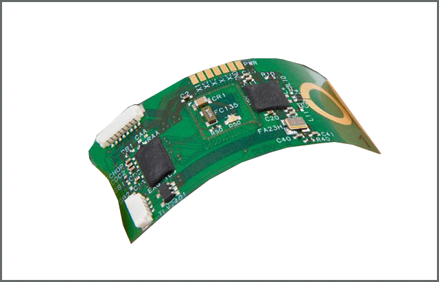
Figure 2 – Flexible PCB
Combining flex and HDI approaches to PCB designs allows companies to create tiny mobile devices plagued less by factors like thermal stress and signal loss without compromising performance. IoT devices can now be smaller, lighter, and faster than ever.
Fabricating PCBs For IoT: What’s Different?
Although the Internet of Things has not necessitated a complete reinvention in PCB development, it has brought new considerations to the design table.
Because of varying design approaches, the layout, fabrication, and assembly process of an IoT-based PCB differs significantly from that of a traditional board.
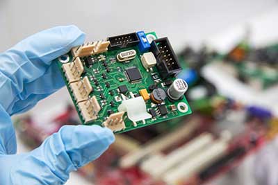
For starters, IoT PCBs typically consist of either rigid-flex or flex circuit assemblies, contrary to traditional boards’ substantially larger and flat nature.
Fabricating with flex assemblies demands extensive, highly accurate calculations of bend ratios, lifecycle iterations, signal trace thickness, rigid and flex circuit layers, copper weight, stiffener placement, and the heat generated by the components.
Moreover, developing PCBs for IoT requires that designers assure robust adhesions between layers on both rigid and flex sides and have a solid understanding of remarkably tiny components like 0201 and 00105 packages.
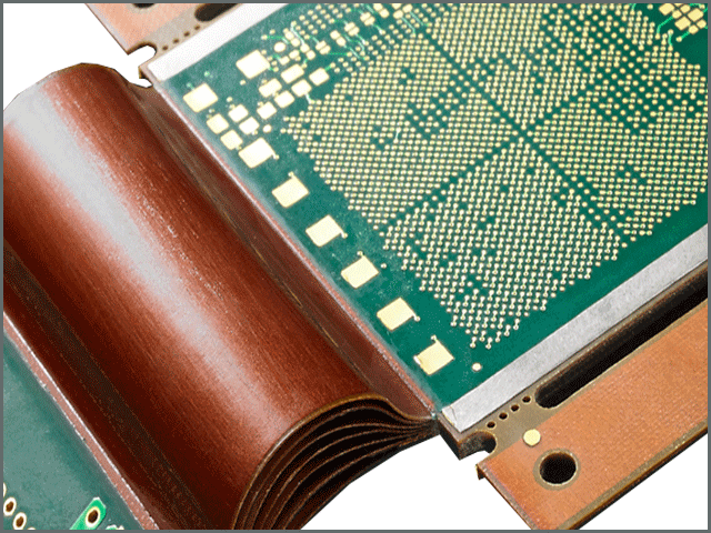
Figure 3 – flex and rigid circuit boards which are connected permanently. When Rigid-Flex HDI Design
Specialized tooling and fixtures are necessary for the proper printing of PCBs meant for IoT devices. For instance, working with a rigid-flex PCB means the developer needs a unique accessory to keep the board utterly flat for effective printing over the different thicknesses of the rigid and flex circuit portions.
Specialized tooling and fixtures are necessary for the proper printing of PCBs meant for IoT devices. For instance, working with a rigid-flex PCB means the developer needs a unique accessory to keep the board utterly flat for effective printing over the different thicknesses of the rigid and flex circuit portions.
Therefore, many IoT startups and new designers partner with specialized EMS companies for their PCB development needs to ensure successful and timely product launches.

PCB Development–IoT And The Future Of PCB Design
The Internet of Things offers the PCB industry many future endeavors, and although circuit board developers are already making good progress with the technology, much more is yet to come. Here are some unique ways IoT is influencing the present and future of PCB development.
1. Diminishing Layouts
The advent of sophisticated IoT devices marked an end to the days when developers had more than enough space to lay down tracks, components, and vias. IoT trends dictate that manufacturers give as much functionality as possible to small gadgets to be worn, pocketed, or even ingested.
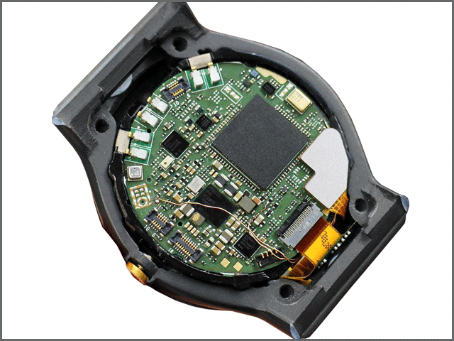
Figure 4 – Smartwatch PCB
Take, for example, the current crop of smartwatches. Despite being just as big as your average wristwatch, devices like the Samsung Gear S3 and the Apple Watch pack hardware like LED displays, internal memory, SoC controllers, Bluetooth chips, and many sensors.
Customers expect more and more from their small, day-to-day devices, and future PCB designers will have even tinier gadgets to work with than smartwatches. Going by the general use of rigid-flex and HDI PCBs, the average circuit board will hardly be acceptable in the coming years.
2. Better Packing Technologies
Through-hole and surface-mount packing formats may have been thoroughly practical over the years, but as gadgets continue to shrink, developers are finding the need to explore newer technologies. One of these is Multi-Chip Modules (MCM), which enables designers to connect multiple ICs on a single die, keeping form factors thin.
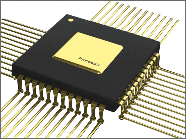
Figure 5 – Multi-chip Module
Another model, System-in-Package (SiP), integrates digital, analog, and RF systems into a single multi-functional chip. At the same time, three-dimensional integrated circuits (3D-ICs) allow the stacking of multiple silicon dies together for a smaller footprint and reduced power consumption.
The impending explosion in the use of these packaging models is set to add immense complexity to printed boards, potentially ushering in a new generation of PCBs, or integrated component boards (ICBs) as they will be so-called, that offer manufacturers a much higher price per surface area ratio.
3. PCB Development—Encompassing Designs
PCB developers are used to designing a board and handing it off to the mechanical team for a fit check and the packing group for the final fitting.
In the world of IoT, however, the smaller form factors and more sensitive components make it crucial for every stakeholder to be on the same page from the beginning of the design process.
PCB fabrication and fitting calculations must be done simultaneously to harmonize function, form, and business needs.
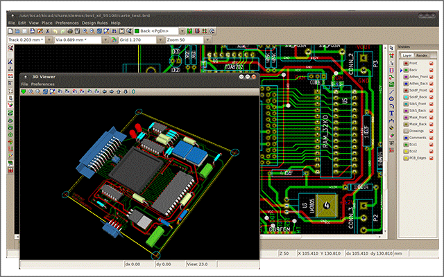
Figure 6 – PCB Virtual Prototyping with KiCad
With IoT rapidly gaining ground, PCB designers should expect to do a lot more virtual prototyping to evaluate parameters like board size, the overall weight of the product, and the board’s fit within the intended enclosure, before tackling the details of the circuitry.
PCB makers will no longer be just another temporary set of hands in a product’s development cycle but rather experts that focus on all aspects of the design process.
4. PCB Development—Standardization
Although standards governing the design of traditional PCBs are already in existence, the Internet of Things is pushing the industry towards an even more uniform future. PCBs made for IoT will need to uphold the highest levels of efficiency and reliability.
Therefore, rather than reconstructing their circuitry to achieve extraordinary results, designers will likely opt to reuse blocks that have already been simulated and proven successful in the field.
Saving and reusing will become the norm in board development, and module design will replace traditional schematic processes.
5. Collaboration with Mechanical Designers
In addition to virtual prototyping and product planning, developing PCBs for IoT necessitates firmer cooperation between circuit board designers and mechanical engineers.
Future product design processes will likely dump the age-old assembly line model in favor of an approach where mechanical and circuit changes and modifications happen in real-time.
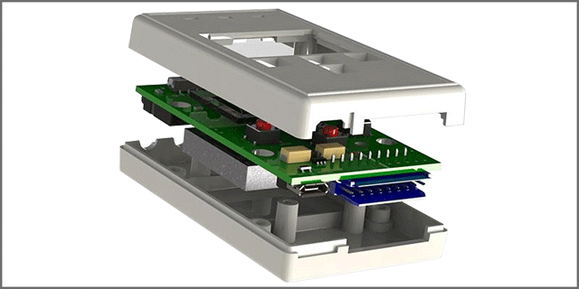
Figure 7 – Electrical-Mechanical Integration
Designers will no longer need to convert files from one software format to the next to share board outlines and component models for basic interference checks.
Instead, mechanical and electronic engineers will embrace the use of ECAD and MCAD tools that bring their data closer together for seamless, real-time collaboration.
Of course, this impending eventuality raises significant concerns for most players in the ECAD industry, whose design utilities don’t work well together, let alone with MCAD software.
The best tools for future IoT design will get engineers and designers on the same page.
6. PCB Development–New Materials
In the modern world of IoT, circuitry must be small; WellPCB offers DC motor controllers in both domestic and international markets. We have a flexible and mobile. As a result, the use of FR4 for square-shaped PCB manufacturing is gradually paving the way for new materials like flex-rigid copper, plastic, and even mesh.
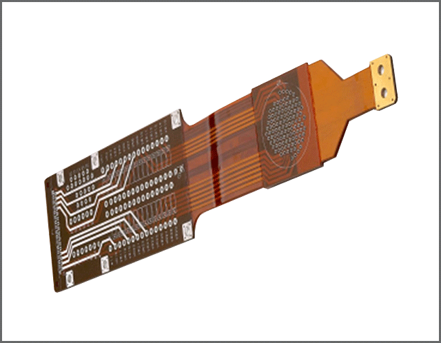
Figure 8 – Rigid-flex Copper
Down the road, FR4 designers will need to partner with specialists that know how to work with alternative materials.
Research firms like Holst Centre and Wearable Technologies are currently the top choices for IoT developers looking for consulting and testing services for wireless autonomous sensors and flexible circuitry.
7. More Emphasis On Wireless Connectivity
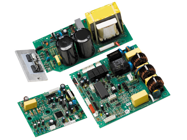
Figure 9 – Wireless Transmitter Module
Wireless modules and RF circuits give IoT products the crucial ability to communicate with their surroundings, collect data and send it to online and offline servers.
Today, the market is filled with IoT-friendly modules and RF components, all of which keep their footprints small while including as much functionality as possible.
As the world’s connectivity needs evolve, however, wireless technology will find its way into more and more gadgets, and PCB designers will have to deal with the challenge of fitting more robust and reliable modules into much tinier boards.
The protocols that dictate ranges, data transfer speed, and security will likely need to be revised and updated to cater to emerging needs.
Even more exciting is that, with standardization becoming the norm, it is entirely possible to have one primary wireless protocol ruling the IoT world of the future.
8. Sharper Focus On Power Consumption
Future IoT products will likely do away with physical power ports and plug-in sources in favor of batteries and energy-harvesting capabilities to promote portability, along with artificial intelligence.
The IoT market is yearning more and more for smart devices that work continuously and with little to no human intervention. PCB designers will, therefore, need to lay more emphasis on energy efficiency to succeed in the future.
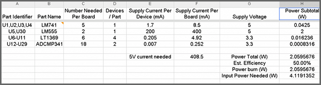
Figure 10 – Power Budget
A promising approach towards better power consumption will be a power budget for individual functional blocks on PCBs instead of considering the product as a whole. That way, designers will gain the much-needed flexibility to identify and refine power-hungry components.
9. PCB Development—PCBs For The Human Body
The health and fitness electronics pool expands every year as IoT developers uncover new ways to make daily life better. However, the human body presents some unique challenges to PCB designers.
For instance, the highly lossy nature of our bodies means that any device intended to be worn or pocketed needs to maintain a solid signal to overcome the noise.
Moreover, because moisture and circuitry do not mix, designing IoT wearables requires developers to consider the effects of sweat and water carefully.
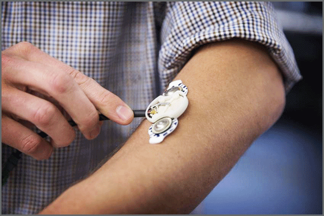
Figure 11 – The Ultra-Low Power PsiKick Monitoring Chip(from phys.org)
Mechanical engineers are playing a significant part in developing packages that are resistant to moisture. Still, as more uses for IoT gadgets crop up, PCB designers will need to do much more to ensure sensitive components are well protected.
10. PCB Development—A Firmer Take On Reliability
Miniaturized IoT devices require a great deal of precision to fabricate. While most designers are typically comfortable swapping fried through-hole components on traditional circuit boards, the IoT market has no tolerance for failure.
Sensitive devices like wristwatches and hearing aids have to work all the time.
As the demand for IoT products continues to rise, PCB designers must ensure their boards work perfectly out of the box.
That means spending a lot of time in simulation programs like PSpice, carefully optimizing their prototypes for the best performance before embarking on physical fabrication.
PCB Development–Conclusion
Electronic design is going through extensive changes to keep up with IoT. New approaches are taking center stage, and PCB makers are gradually embracing product development as a whole and not just the design of circuit boards.
As the demand for mighty circuit boards with tiny, lightweight components expands further, the designers and fabricators with the imagination and the expertise to take advantage of the emerging opportunities will benefit profoundly.
So, are you a player in the IoT game? Would you like to partner with a company that knows the ins and outs of PCB development for the Internet of Things? Reach out to WELLPCB Limited and get on the right track today.