Contents
- 1 Getting Started with Building Your PCB Prototypes
- 2 Making A Printed Circuit Board for your PCB Prototypes
- 3 Manufacturing your Printed Circuit Board using WellPCB
- 4 WellPCB PCB Capabilities and Some Common PCB Terms
- 5 Moving from PCB Prototypes to PCBA
- 6 Saving Money in PCB Prototypes and PCBA Manufacturing
- 7 Conclusion
Getting Started with Building Your PCB Prototypes
So now you have this fantastic idea or, better still, a PoC (Proof of Concept), but you need to scale to something worth mass producing or at least can be fabricated by some manufacturers for demo purposes; how do you get started with building your PCB prototypes?
In hardware design, PCB prototypes are a “hand-built” model that represents a manufactured (easily replicable) product sufficiently for designers to visualize and test the design.
The word prototype comes from the Latin words proto, meaning original, and types, meaning form or model.
With all the tutorials out there and the number of free resources available, it’s becoming possible for almost anyone to build quick PCB prototypes in a couple of hours.
Bringing your PCB prototypes to a place where they can be commercialized takes a lot of effort, planning, and expertise.
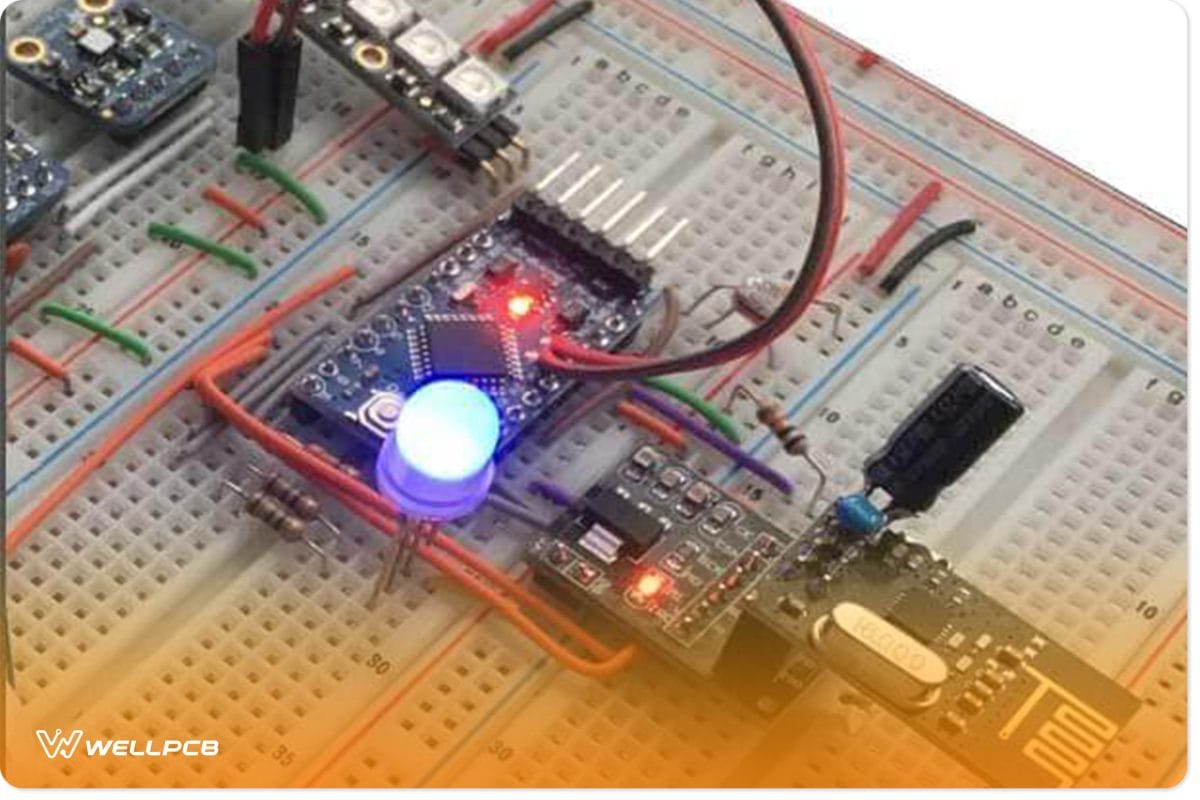
You have to make a host of decisions about hardware, which eventually drive decisions about the device software. Breadboard PCB
It’s easy to build with a Raspberry Pi or even the popular Arduino, but the chances you can mass produce with those are mostly limited.
Of course, this doesn’t mean you can’t possibly build a board on the Arduino board like the Arduino Pro Mini or those headless Arduino can plug into it and then go on fabricating something like that.
Still, they can get quite expensive and could even be more powerful than you need.
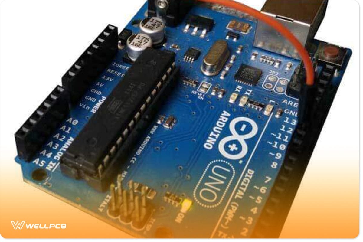
Many of today’s hardware startups have built their first PCB prototypes with Arduino. Arduino is easy to learn, even without an electrical engineering background or only the necessary programming skills. Even a child could do it, and many of them do.
Components Selection
The first step in getting started with building your PCB prototypes is knowing what components you will need.
You can quickly get an idea of those based on your block diagram or existing PoC, and even the device’s desired functions can promptly tell that.
For example, building something like a wearable heartbeat monitor will require some of the following:
1. A Microcontroller unit – Atmega, ARM, PIC, and others
2. A Pulse sensor – A dedicated pulse sensor might work, or a combination of LED and Light detectors could work as well.
3. Powering Unit
4. A display interface – LCD, LED, OLED, TFT, or others.
One can easily outsource most, if not all, of the needed parts from a single electronics supplier and, in some cases, from multiple suppliers.
The following are some suppliers you can buy your details from – AliExpress, Digi Key, Arrow, Mouser, Adafruit, and several others.
Schematic Design
The next step will be to create a diagram of the electronics design, usually called a schematic diagram or a circuit diagram.
The schematic drawing shows how every component connects, and this is not something you will do by hand but a unique tool designed for this purpose.
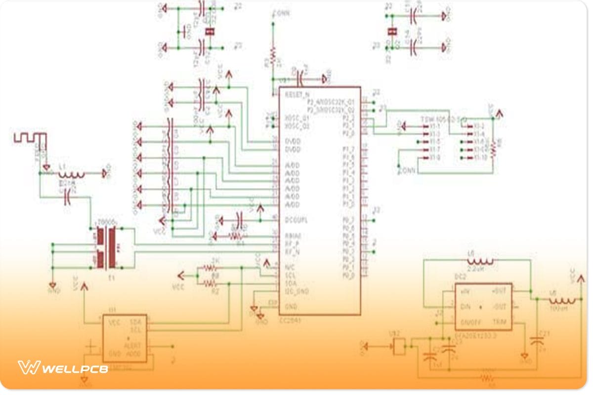
Creating a schematic is a core step in building your final device, and you can’t afford to skip it.
Getting started with your schema is very easy; you need to know the right tool to build.
Several circuit design software programs can be used for schematic design; some are free, and some are paid.
Most design software can be used for schematic drawing and also for making your PCB layout.
Below are some software to be used:
1. KiCAD – Free to use.
2. Eagle CAD – Premium but with the limited free option
3. Altium – Premium
4. DipTrace – Premium
5. OrCAD – Premium but offers a free trial.
After deciding on the design software to use, one can familiarize oneself with the software environment since each software might have a different look and feel.
When creating your schematic on your software of choice, one must follow some standard practices in schematic design.
Some conventional methods are highlighted below –
1. Using a junction dot to indicate more than one connection that connects in a junction.
2. Use a net name for pins rather than drawing hundreds of connections around them. This enhances the readability of a schematic without adding unnecessary clutter.
3. Always using the same symbol for the same device
4. Separating your schema into logical blocks, especially when designing some complex circuits.
When you are done with your schematic design and have fully cross-checked it, the next step will be to convert the circuit design to manufacturing PCBs; there are high chances of layout failures, which can go a long way into negatively affecting the final product’s functionality.
Several PCB layouts will be used to manufacture your board.
In the next chapter, we talk about making a printed circuit board for your PCB prototypes.
Making A Printed Circuit Board for your PCB Prototypes
Making A Printed Circuit Board for your PCB Prototypes,
first, having a schematic diagram is one step of the process of having a full-fledged professional board.
The next stage of the process, which is the one that can’t be skipped, is designing the layout of your printed circuit board. However, what is a Printed Circuit Board?
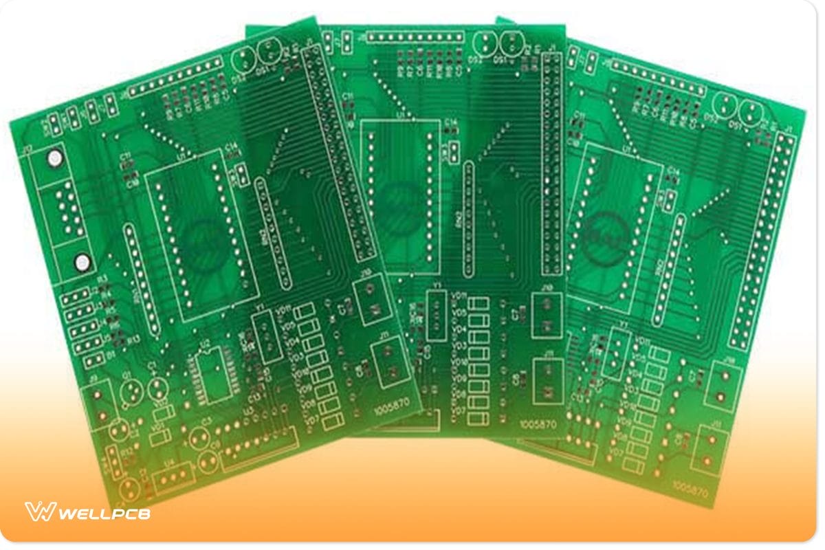

A Printed Circuit Board, otherwise known as PCB, is a physical board that holds and connects all of the electronic components in one place.
The schematic design is usually transferred to the PCB using several methods. The design of the PCB influences some factors, like
1. Cost – The more significant the board, the more expensive it is to make.
2. Performance – The board design and the type of components used will affect the device’s overall performance. A poorly designed board might be susceptible to noise, which in turn degrades the performance of the device.
3. Durability,
4. And many more.
Once the schematic is ready, we move to make the PCB.
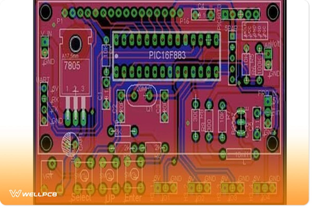
The PCB is designed with the same software that was used in creating the schematic diagram.
The software will generate the PCB layout and footprint based on the given components and schematic diagram; without the schematic diagram, the software will not create the basic PCB layout.
Getting started making a PCB layout might be time-consuming and tedious for first-time users.
Still, fortunately, there are several handy tutorials and resources online for most PCB software in learning how to build them.
Depending on the software of choice, there is usually a way for the user to switch from the schematic view to the PCB layout view where the PCB will be designed.
Design your PCB as you envision your final device model. The software will have various verification tools to ensure the PCB layout meets the design rules for the PCB process used and matches the schematic. You can quickly test whether your design will break your device or not.
The smaller the product and the tighter the components must be packed together, the longer it will take to create the PCB layout.
If your product routes large amounts of power or offers wireless connectivity, PCB layout is even more critical and time-consuming.
Most PCB prototype designs’ essential parts are power routing, high-speed signals (crystal clocks, etc.), and wireless circuits.
Having complemented your PCB prototype design, you should go ahead to manufacture your printed circuit board, and there are several ways to get this done.
Either make it yourself at home or send the design to a manufacturer specializing in making PCBs.
Although there are techniques for producing PCBs at home, they are limited to simple designs. So, you will most likely need to outsource the production of your PCB prototypes.
In the next chapter, we talk about manufacturing your printed circuit board from a third-party manufacturer.
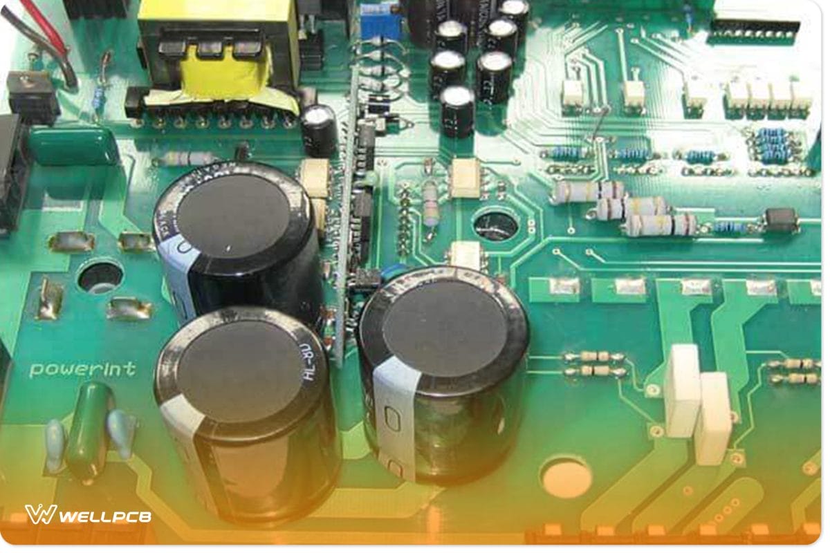
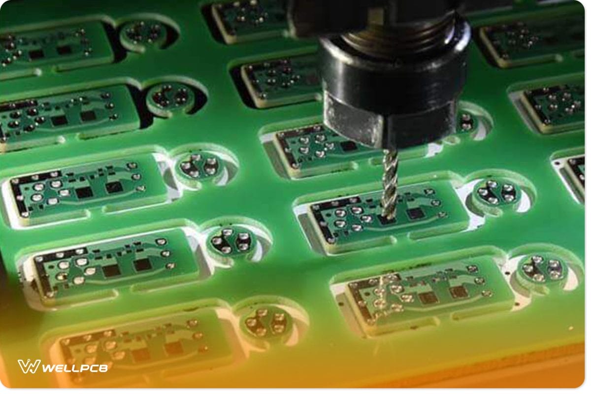
Manufacturing your Printed Circuit Board using WellPCB
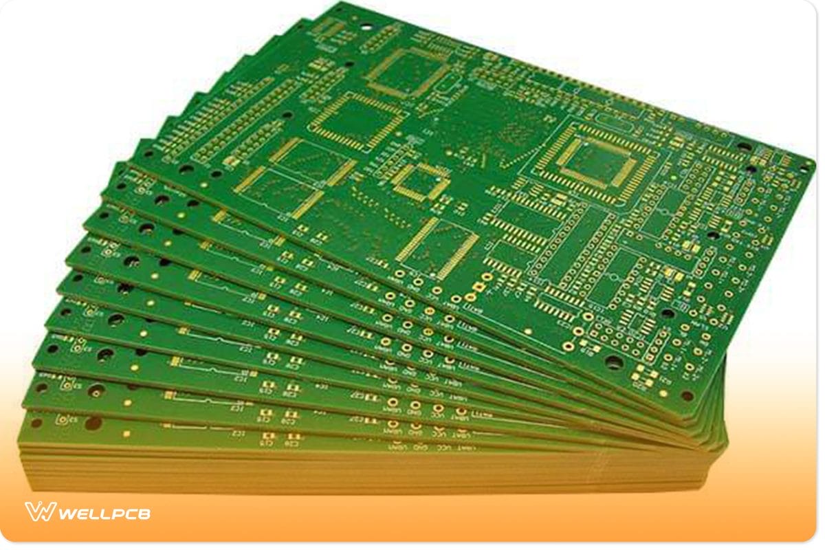
Having successfully developed the printed circuit layout for your device, you need to do next to make the board.
Before commencing manufacturing, it’s always a good idea to see how the final product will look.
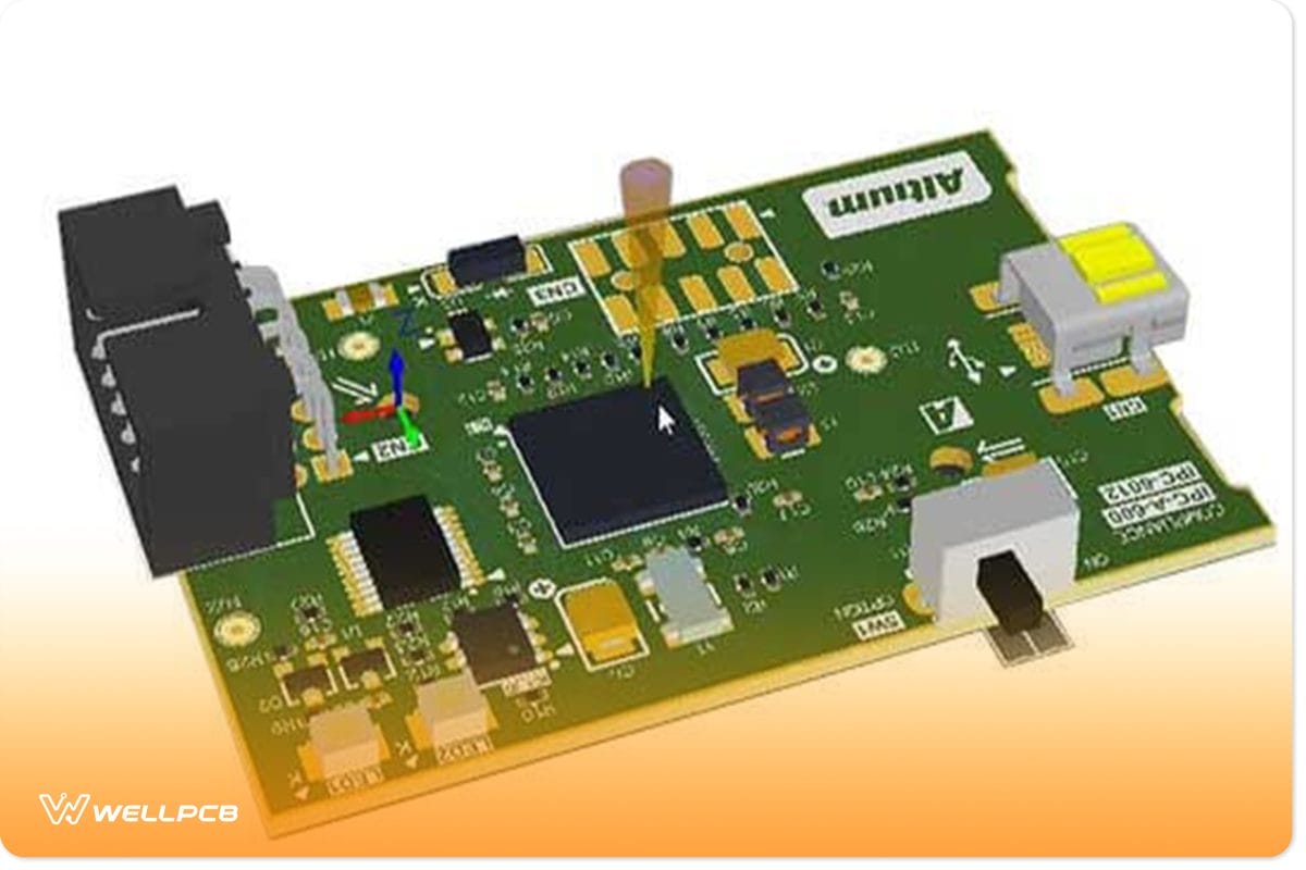
Some software like Proteus or Altium has a 3D layout viewer that will allow one to view the board in 3D to feel how the board will look.
Before sending your design to be manufactured, you first need to generate a file format that the manufacturer will work with and decide what to use.
WellPCB is a leader in manufacturing.
Printed Circuit Board and the best bet for your PCB making jobs.
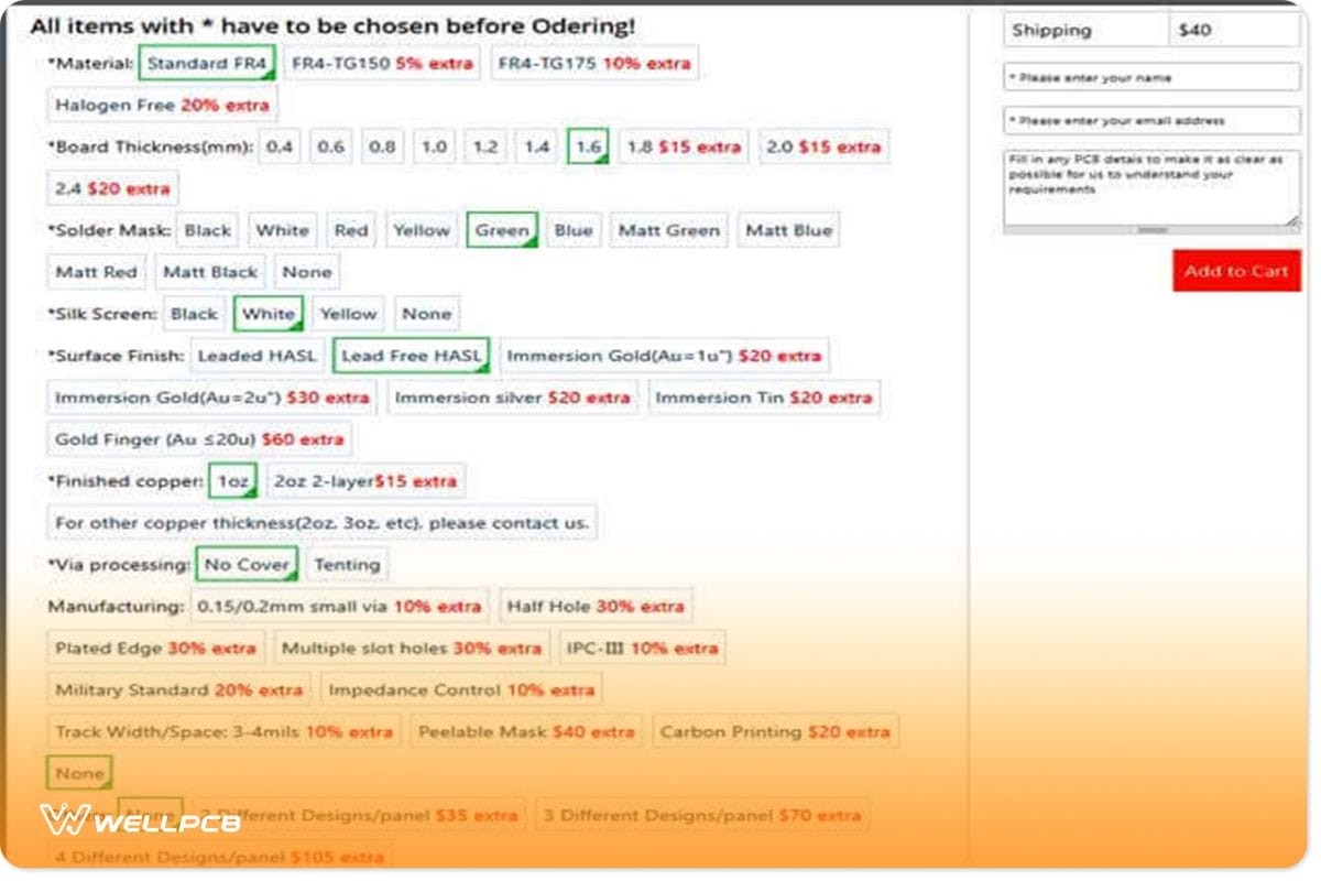
The PCB design must be converted to a Gerber file that most professionals use, the standard for the PCB industry.
A Gerber file contains all of the necessary design files to use in the PCB’s production. WellPCB accepts four file formats (Gerber, pcb, pcbdoc, or cam file format).
WellPCB prints a silkscreen on both sides, and it comes without any extra charge. It’s helpful to include part numbers on the printed silkscreen layer.
It’s also a good idea to know the board house specification.
WellPCB has a minimum of 3mil for line/track width and space. Ensure your design doesn’t exceed that. Use your software design rule check to ensure your board doesn’t exceed the manufacturer’s production abilities.
Silkscreen requirements state the desired color on the PCB, and most are UV-cured inks and are RoHS-compliant.
1. White
2. Yellow
3. Black
Those are the most widely used colors; others are also available, and colors can add to process time and cost.
To order for your PCB on WellPCB, you follow these easy steps:
4. Visit the WellPCB PCB Online Quote Section – https://www.wellpcb.com/pcb-quote
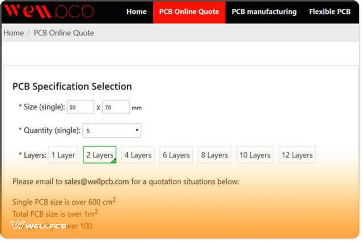
5. Fill in your board details and click add to cart. Need to know about ordering custom PCB Circuit boards online. For the PCB board you need, you can contact us at WellPCB minimum quantity is five units of PCB
6. Register a new account.
7. Upload your PCB Gerber or. Brd files.
8. Order your item and wait for it to be delivered.
WellPCB also helps perform a full DRC check of all client files, which is helpful, especially if the design has some issues or errors.
The user will be alerted of the problem to avoid wasting time and money during the production of the board.
Now, you sit down and wait for your printed circuit board to arrive. The PCB fabrication lead time for its PCB services is at least 24 hours and a minimum time of about 120 hours for an 8 – 12 layer PCB.
In the next chapter, we will be talking about some of the PCB terms and WELLPCB capabilities.
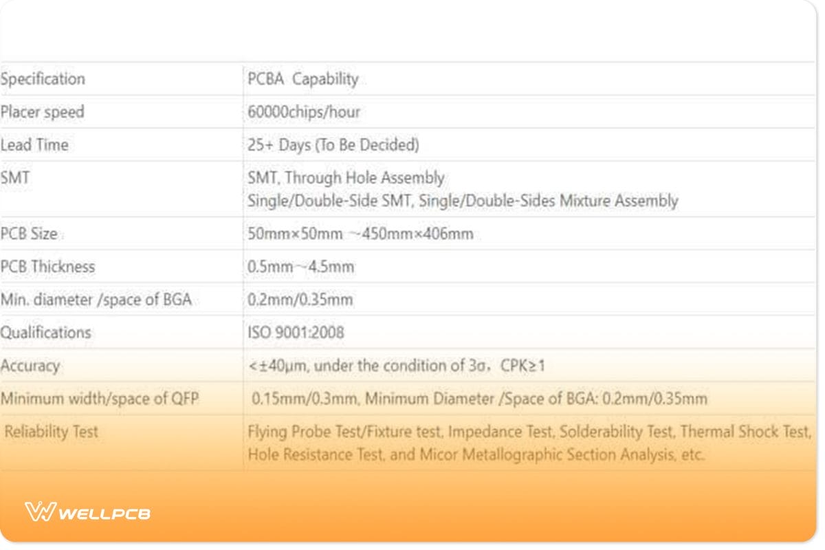
WellPCB PCB Capabilities and Some Common PCB Terms
WellPCB is a leading manufacturer of printed circuit boards and offers printed circuit board assembly to accompany its PCB prototypes.
This makes WellPCB your go-to manufacturer for your entire product development. Also, they provide Turnkey services for outsourcing the components for your electronic board. Breadboard PCB
WellPCB is focused on offering PCB prototype services and not just large-scale manufacturing. Their PCB prototype services go at a minimum of 5 units. Not only are they offering prototyping services, but they are also packaged at meager prices.
A promotional price of $3.99 for users looking for 1-2 layers, 10pcs PCB prototypes, and a board of less than 10cm*10cm.
WELLPCB is capable of producing 100,000 square feet of 2-32-layer PCBs and delivering over 5000 varieties monthly.
With a quick turn to meet 24-hour delivery for double-sided PCBs, 48-hour for 4 to 8 layers, and 120-hour for 10 layers or higher PCBs. Their standard lead time is about 5 – 6 days, and an Expedited time of 24 – 48 hours.
The following are WellPCB PCB manufacturing capabilities
1. Support Material: FR4, High TG FR4, Halogen Free material, CEM-3, Rogers HF material.
2. Layer counts 1-32 layers.
3. Finished Copper Thickness: 0.5-5 oz.
4. Finished Board Thickness: 0.2-6.0mm.
5. Min. Line/Track Width: 4mil.
6. Min. Line/Track Space: 4mil.
7. Min. Contour Tolerance: +/-0.1mm.
8. Min. Finished Diameter of PTH Hole: 0.1mm.
9. Max. Board Thickness/Hole Ratio: 12:1.
10. Min. Solder Mask Bridge: 4mil (Min. SMT Pad Space 8mil).
11. Min. Legend(Silkscreen) Track Width: 5mil.
12. Solder mask color: green, black, blue, white, yellow, matt, etc.
13. Solder mask hardness: 6H.
14. Legend/Silkscreen Color: white, yellow, black, etc.
15. Surface Treatment: HAL, Lead-Free HAL, Immersion gold, OSP, Immersion Tin, Immersion silver, etc.
16. Other Technology: Gold finger, peelable mask, Non-across blinded vias, characteristic impedance control, Rigid-flex board, etc.
17. Reliability Test: flying probe test/fixture test, impedance test, solderability test, thermal shock test, hole resistance test.
18. Flammability: 94V-0.
Surface Finish
A PCB surface finish is a coating between a component and a bare board PCB. It is applied for two primary reasons: to ensure solderability and to protect the exposed copper circuitry.
Standard surface finishes preference – Non-RoHS or RoHS compliant.
1. HASL (Hot Air Solder Level) – Contains Lead non-RoHS, cheaper and quite popular.
2. ENIG (Electroless Nickel Immersion Gold) – MoThe most popular finish and lead-free but expensive
3. Immersion Silver – RoHS compliant will tarnish like any silver product
4. OSP – Organic Solderability Preservative
5. LF-HASL (Lead-Free Hot Air Solder Level)
6. Immersion Tin – Used the least of all finishes
Soldermask
Soldermask is the color to be used for the PCB prototype finish. Any color can be used. However, sticking to standard colors is the best and most professional. The most popular are:
1. Green
2. Blue
3. Black
4. Red
5. White
6. Yellow
The mask can be in either Matte or Gloss in those above colors. Matte is less readily available due to Gloss is the most widely used. Processing Matte for specific colors may add time due to equipment changes and processing cleans and applications.
Silkscreen
Silkscreen is the printing done on the PCB for identification. It is used on the component side to identify components, test points, PCBA part numbers, warning symbols, company logos, and manufacturer names. The following are some of the colors being used:
1. Black
2. White
3. Yellow
Those are the most widely used colors; others are available; however, colors can add to process time and cost like MASK. Ask if you have special requirements for your product.
In the next chapter, we will talk about how to move your PCBA mode.
Moving from PCB Prototypes to PCBA
So, what’s PCB Rapid Prototyping? PCB assembly. Directly speaking, PCB Rapid Prototyping. PCB assembly.
Directly speaking, PCB Rapid Prototyping. 3D PCB Printing makes the PCB and does the Printed Circuit Board Assembly (PCBA, an abbreviation for printed circuit board assembly, which refers to the combination of PCB prototype manufacture, components sourcing, and B3D PCB Printing makes the PCB and the Printed Circuit Board Assembly PCBA is the PCB with components assembled).
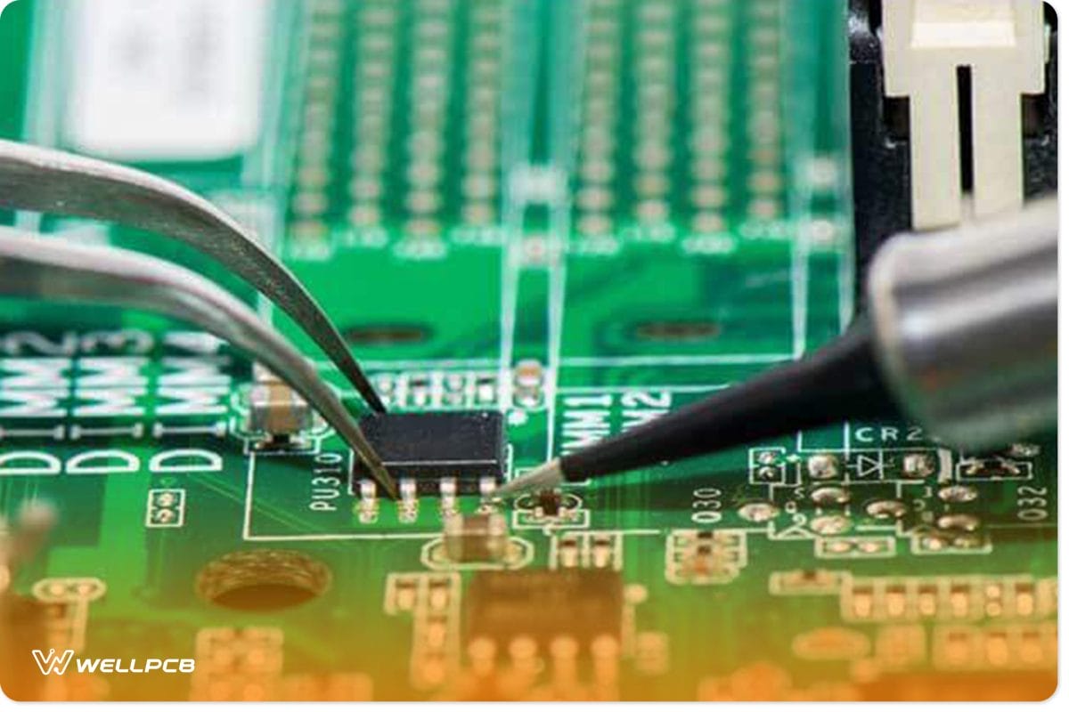
So now you have your printed circuit board available and ready to populate the board with the needed components. You might be tempted to solder this manually yourself.
This might be a good option, especially when the number of panels is less than five or, worst case, ten units; anything more than that might not be a good idea, but going the route of PCB Rapid Prototyping.
3D PCB Printing not only makes the PCB but also does the Printed Circuit Board Assembly PCBA.
Assembly Types of PCBA
The main assembly types of PCBA are shown below:
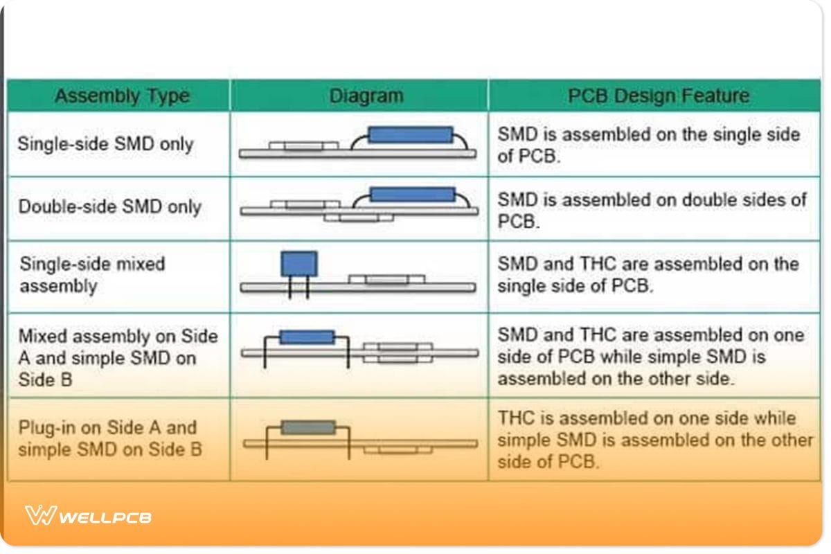
Those are the commonly used PCB Rapid Prototyping. 3D PCB Printing makes the PCB and does the Printed Circuit Board Assembly (PCBA assembly types. SMD means Surface Mount Devices, and THC implies Through Hole Components).
PCBA helps engineers, product developers, hobbyists, and others to self-populate the board with needed components by a manufacturing firm.
It is usually faster and cheaper on bulk orders. Getting started with PCB Rapid Prototyping.
3D PCB Printing makes the PCB and does the Printed Circuit Board Assembly (PCBA is also relatively simple as far as you have the necessary resources).
Just like WellPCB is capable of handling all your possible PCB prototype works, they also offer an accompanying production film work that you require to manufacture PCBs.
In the case of PCBA service, it helps one streamline the whole board development process.
It does not cost much more to have the PCB populated unless you tack on additional steps in the process, such as burning a program to the MCU or running a 100% test on the finished boards.
To get started with PCBA, you need to have all the required documents.
Aside from your PCB prototypes design file, you will need a design specification if there are special needs for your work, a bill of the material (BoM) list for the number of components on your board and also can be generated from the software being used, and part placements made from the software used.
When starting your PCB Assembly, one crucial thing to take note of is the sourcing of the components for the board.
The board owner can decide to source for the parts alone and send them to WELLPCB for assembly or let WellPCB handle the integral components sourcing, which I feel is better.
Of course, partial supply can also be agreed upon.
Go to PCB Assembly on WellPCB here and fill out the Request for Quotation (RFQ) form. Input as many details as possible and send it.
WellPCB will get in touch if they need more information from you and continue the assembly process order.
The WellPCB Bill Of Materials (BOM) of a PCB gets fitted aboard. PCB Assembly process can take up to around 25 days for large volume manufacturing, which is an excellent time for large volume PCB assembly compared to other PCB Assembly manufacturers.
This will make it easy for a pick-and-place machine to easily pick and place the components on the PCB Assembly capabilities:
More information about WellPCB SMT). This will make it easy for a pick-and-place machine to easily pick and place the components on the PCB. Assembly capability can be found here.
At this point, all you have to do is sit down and wait for your populated PCB to be available and sent to you.
This concludes the end of this chapter, and the next chapter will discuss how to save money when doing PCB and PCBA.
Saving Money in PCB Prototypes and PCBA Manufacturing
Now, congratulations, you have your fully developed hardware PCB prototypes or, better still, hardware board.
For newbies, this will have been a good experience, and also a lot of money must have been sent, which could have been avoided.
Some of the money spent could have been avoided due to unnecessary complexity and errors in the PCB and circuit design.
This chapter will show some of the handy tips and tricks that can help you save even millions when doing large volume manufacturing.
Keep Your Board Size at a Minimum
Keeping your board size at a minimum is crucial in saving costs and making your final product as portable as possible.
The bigger it gets, so do the prices. If the board becomes smaller, so does the cost.
Also, making your board too small might not save you cost since assembling and preparing your board might require specialized equipment.
Using Surface Mount Components as Much as Possible
You might be tempted to use a DIP (dual in-line) package, commonly known as Through-hole components, because it’s easy to use but might not be the best cost-saving option.
1. Using surface mount components will reduce the number of holes that need to be drilled on your board, typically used for through-hole parts.
2. Using surface mount components will also reduce the board size.
3. Using surface mount components will make the board assembly faster and lesser equipment used.
Set Your Design Up for Penalization
By going on board penalization, you can save yourself a ton of money.
Getting all of your boards on one panel means that a rapid-fire pick-and-place machine can get all your parts placed in one go without requiring any additional setup time.
Silk Screening Helps You Reduce Your PCB Prototype Costs?
Requesting silk screening on one side will cut your artwork costs in half. Sticking with standard colors and larger geometries will also prove beneficial.
Understanding these constraints can help you to better PCB prototype pricing and cost savings.
Use the Right Via for the Job
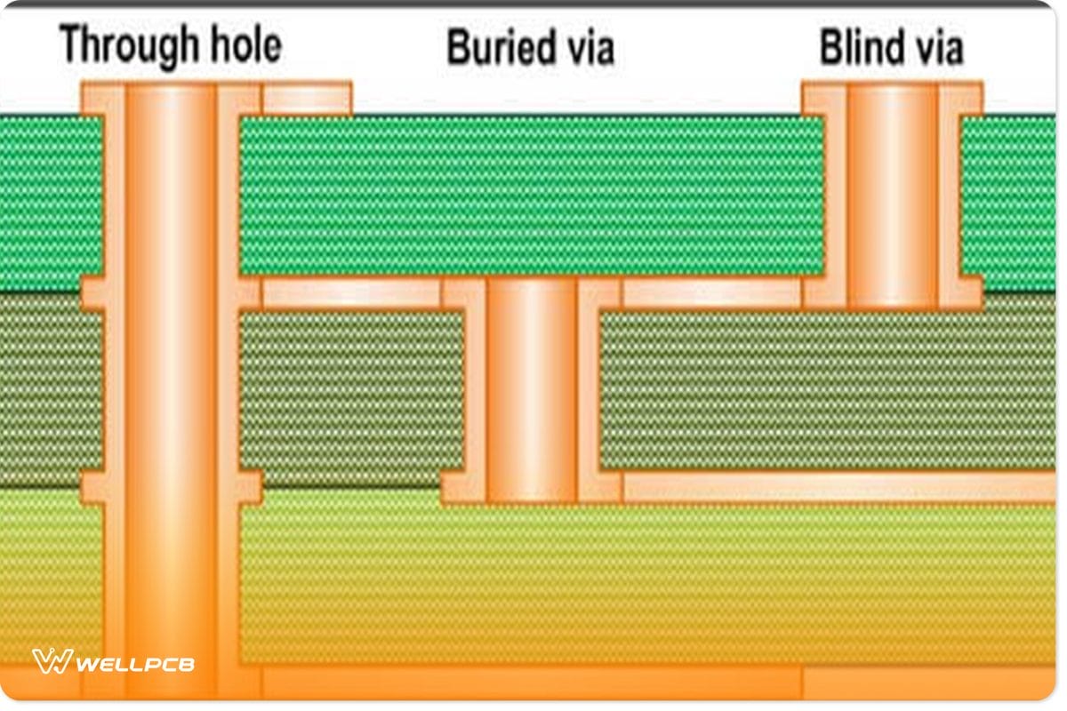
There are three types of vias – through-hole vias, blind vias, and buried vias. The last two are only going to be used for high-density and high-frequency PCBs.
So, this one is simple: if your design doesn’t need these types of vias, leave them out to avoid any extra manufacturing costs.
This concludes the end of this chapter and the end of this guide.
Using standard materials and several of these tips mentioned above can save you several thousand to millions of dollars when embarking on large-volume manufacturing.
Conclusion
When building and launching your products to market, some other things also need to be considered.
1. Certifications – Every wireless-based product needs to go through some certification process to be clear of any hazards or issues and be permitted to the market.
2. Enclosure – Depending on the type of product you are building, you might need some enclosure around your board to give it some artistic look or for some reason.
3. Quality Control – Quality control issues a formal inspection report for review and shipment approval.
You should expect each shipment to be inspected and approved before being released. Such a protocol creates a closed-loop process that builds in continuous improvement for consecutive production runs.
This guide should give you enough head start in launching your following product.
Taking an idea from concept to production is not for the faint of heart.
You have to withstand failures, criticism, and mishaps, and managing the whole manufacturing process can be very challenging.
Still, a manufacturer like WellPCB is in the business to help you succeed.