Contents
What is PCB Silkscreen?
Think of roads and streets on a map—they’re only useful if you can see text and legends identifying where each connection leads.
In a PCB, silkscreen serves this same purpose. It provides essential text-based information on various circuit points, components, and other crucial details about the circuitry, making it easy to understand and troubleshoot.
For a flexible PCB, silkscreen plays an equally vital role, helping identify specific components and connections on boards that may need to bend or fit into compact spaces.

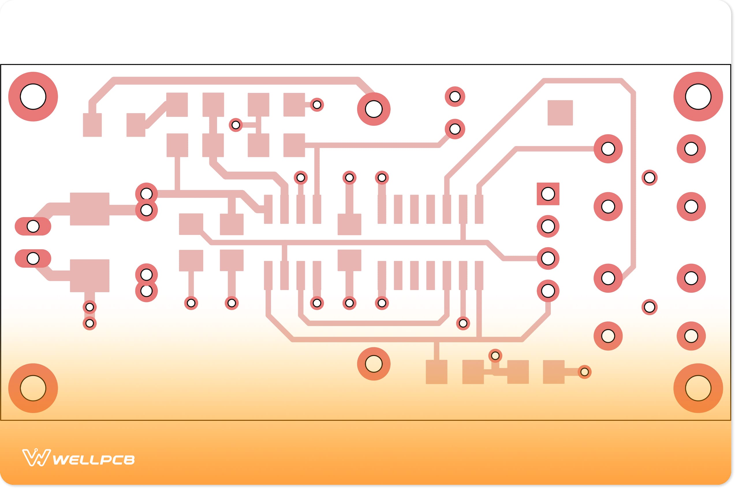
Figure 3: Yellow PCB-Silkscreen
You should understand that PCB silkscreen is just one process of overall PCB manufacturing.
Technological advancement allows the text and beautification images to be part of silkscreen artwork design.
However, the pitfall is that you may overlook the fundamental purpose of the design and may make the information unreadable easily.
Therefore, You must keep the primary goal of silkscreen in mind while creating the artwork.
Now that you have developed a basic understanding of PCB silkscreen let’s examine its significance in overall WellPCB.
We have ten years of experience in the PCB manufacturing process. We will provide you with a one-stop service and high-quality products.
You can send us the documents you need to make and get a quote immediately! What are we waiting for?
Significance of PCB Silkscreen

First, let us remind you of the primary use of PCB. Also known as Print Wiring Board (PWB) or Engraved Wiring Board, PCB provides mechanical support to connect the various electronic parts in a circuit board electronically.
It uses conductive pathways, signal traces, or tracks imprinted from copper sheets laminated onto a non-conductive substrate.
Components and conductive paths are spread all across the board without identification.
This requires you to place customized information to help the end user/customers.
- Print company logos like the name of the company that made the product,
- Warning signs like High Voltage,
- Version numbers like V2, V3, etc.
- Manufacturer identifiers,
- Testing points,
- Part numbers,
- Components orientation,
- Processing types, etc.
In a broader perspective, you can say that the role of PCB Silkscreening extends to but not limited to
- Circuitry identification includes testing points, ground points, component interconnects, etc.
- Troubleshooting of circuits in case of a burnt part or undesired result produced.
- Parts identification in case of replacement required or design evaluation needs to be done.
- Safety precautions by putting in warning signs like high voltage, grounding, etc.
- Branding and publicity of manufacturer. It can also serve as protection against illegal copying of circuit design.
- Product evolution, such as component replacement testing or rating verifications.
It may be noted that silkscreen information depends on the board size of the PCB you choose. If you have limited space available, you should prioritize the critical data.
This becomes more critical if you have selected a flexible PCB design for your project. The
The PCB silkscreen process impacts the overall quality of the PCB. Once you understand the process, as described in the next chapter, you can learn more about it.
Process of PCB Silkscreen
PCB silkscreen is a subprocess in the board tree of solder masking and baking, UV exposure, and development. However, due to its overall impact on the product’s grading and reliability, it can be considered the most sophisticated among the four in its class.
Now, PCB silkscreen is a part of the overall PCB manufacturing assembly line.
Overall silkscreen process consists of at most 32 steps, which can be categorized into six broad processing areas.
These processes may vary in actual scenarios depending on the material of PCB elements, quality requirements, and cost.

Figure 4: Automatic Character Ink Printer
3.1 PCB Silkscreen Design using EAGLE
This is the phase where the artwork you designed to be printed on PCB is readied. You can do it very quickly and artistically with the Computer-Aided Design software EAGLE.
It is part of the PCB design package and lets you design your silkscreen layer, h circuitry,y, and other design elements pleasingly.
The rectangle shape of the yellow color represents the silkscreen outline. You can look for it above the grey package dimension lines.
Once the silkscreen menu is selected, it is easier to move ahead with your design.
From parts placement points to text writing can be done through different menu options available. You can refer to the EAGLE Silkscreen tutorial for more details.

3.2 Preparation of PCB board
Once the CAD blueprint is finalized, it’s time to implement hardware. You need to perform some steps to finish the product well.
The first step in this process tree is selecting the type of board for WellPCB. We have ten years of PCB manufacturing experience.
We offer a one-stop service and high-quality products. Send us the documents you need to make and get a quote immediately! What are you waiting for?
The selected material is then picked up for cleaning, followed by tape trolling and board handling. The PCB board is then ready for printing.
At this point, the PCB Designs should be ready and printed (black) on transparent paper.
The designs are placed on the dried silkscreen. In this case, the silkscreen PCB Design should be placed on the prepared silk fabric how you would like the writings or the markings to appear on the PCB.
It is essential to ensure that the PCB Design paper does not move from its position. This can be done by fixing the designs firmly on the surface using TRANSPARENT tape.
When this is done, the whole setup (silkscreen and the attached designs) is turned upside down such that the methods face downwards. The top side is then covered with dark cardboard.
The UV light is shown below for about 15 minutes when the PCB silkscreen artwork is fully developed.
To expose the developed silkscreen template, pressurized water is used to wash away the emulsion parts not exposed to the UV (not cured).
3.3 Silkscreen Printing
In these steps, actual silkscreen printing on the board occurs. The board is fixed on the machine for printing. The screen moves upward, downward, and left in the following four stages, suitable for direction printings. The design you made on EAGLE is now imprinted on PCB.
The ready PCB (already etched) is placed below the silkscreen fabric to print the silkscreen on the PCB. The PCB should precisely align with the silkscreen artwork on top.
Again, after positioning the PCB directly below the silkscreen and aligning it well, it should be fixed firmly in place to ensure that it does not move during the application process. This can be done using stoppers at the sides of the PCB.
The silkscreen UV curable ink, usually white, is applied evenly over the artwork (silkscreen) using a squeegee. The writings or markings are well imprinted on the PCB surface. From here, the PCB is dried for about 10 minutes using a drying oven.

3.4 Handling Procedures
Although printing has been completed, a proper handling mechanism is vital to retain the PCB board’s quality. That is why the highest number of steps are gauged in handling procedures.
As shown in the figure below, around 12 different stages are performed to ensure that silkscreen printing does not affect the quality of the PCB and that the information imprinted on the board meets the overall criteria.
3.5 Inspection Procedure
The inspection procedure is conducted in the middle of the handling steps and at the end of the processing steps. Its purpose is to check the quality of the PCB panels visually.
This procedure ensures that the information on board is correctly readable by the human eye. It would help if you checked for misprints or missing information.
3.6 Treatment of Silkscreen
In the final step, the silkscreen print is treated, and the product is inspected for readiness. Once quality assurance is passed, the PCB with silkscreen processes is completed.

Figure 5: Process of PCB Silkscreen
An emulsion is mixed with the developer in a ratio of about 10:1, preferably done in a dark room. The mixture is then applied evenly on the surface of the silk fabric using a wide squeegee or a similar tool.
It is advisable to apply around two layers on each side to make a total of 4 layers. This layer must be uniform, with no spaces or bubbles.
Please leave it to dry up or accelerate the process using a drier.
One of the dependent factors on which some steps in the PCB silkscreen process tree depend is the Method of PCB silkscreen that you choose. The next section describes methods of PCB silkscreen for your detailed understanding.
Methods of PCB Silkscreen
The choice of the PCB silkscreen method depends on many factors, including time, cost, the precision required, board spacing available, and the material of the PCB used. Each method described below offers a fair trade-off in these parameters to help you with PCB design choices.
4.1 Manual Screen Printing
Manual screen printing is the oldest and most cost-effective PCB Silkscreen method. This process uses epoxy, which is pushed onto the laminate and dried to create an impression on the board.
Setup requirements for manual screen printing are much more accessible. Its cost-efficiency also makes it a preferred choice. Also, the application of manual screen printing still makes it a select option for many tasks.
On the downside, this method requires more board spacing and impression drying due to its support for a larger text size. Pad clearance is another challenge.
It would help if you opted for manual screen printing to cut costs; board spacing is not an issue.
4.2 Liquid Photo Imaging
This process utilizes a similar process that was based on the correct PCB service provider. Thankfully, there have been various PCB manufacturing processes in the past.
The same procedure as the solder mask is used for silkscreening. The difference is that white replaces green.
Laminate is first coated through the epoxy. This epoxy is liquid and has the property of photo imaging. The sketch of silkscreen is transferred to plates through exposure to UV light.
The results obtained from liquid photo imaging are more precise than those from the manual silkscreen process. This method also reduces the required spacing, utilizing the board space more efficiently.
This process requires more ink than the other two processes.
Also, the time needed to set up and more time to apply.
You can use liquid photo imaging to save your project’s space on board and fineness.

4.3 Direct Legend Printing
This process uses the exact mechanism used by paper printers. It uses high-end inkjet printers capable of ink transfer on PCB.
Another ease of using this process is that CAD application data is directly printed on the circuit boards. The ink used in Direct Legend printing has also been upgraded to acrylic to save impression drying time.
Being the most digitalized process, this process has the highest accuracy and best time efficiency. It can have a low text height capacity, but lower than 0.02 inches is not used as it may not remain readable by the human eye.
The downside is that this process cannot be used for boards with the silver material survey. Also, acrylic ink is limited for some applications.
You can gain the benefits of time and board spacing by choosing DLP.
Choosing the proper method of PCB silkscreening helps reduce overall cost. The next section describes other factors affecting silkscreen cost.
Understanding The Cost of PCB SilkscreenDue to fixed cost characteristics,
During the PCB design process, PCB Silkscreen cost is placed under the head of nonrecurring tooling. The silkscreen process contributes around 12-15% of the overall PCB manufacturing costs.
Text design refers to character width, height, thickness, spacing, and placement variations. Artwork cost is usually not separately charged.
The cost of ink depends on the silkscreen method used. Acrylic ink is used for the DLP method, whereas other methods utilize epoxy ink.
Ink cost depends on specific properties such as substrate compatibility, adhesion properties, curing procedure, and acid/alkali treatment immunity.
The color of the ink is also a decisive cost factor. White ink costs less than other colors.
Around 5% of overall PCB cost can be reduced with cost optimization for PCB silkscreen regarding material choice.
The method of silkscreening used also impacts overall cost. Liquid Photo Imaging (LPI) and Direct Legend Printing (DLP) cost more than manual screen printing, as the capital cost of setup is high.
Another vital factor in silkscreen costing is whether you want to print artwork on both sides or only one side. In the case of both sides, the cost jumps up.
You can also consider the DIY option for PCB silkscreen or opt for a manufacturer. This factor also controls the budget, as you desire.
Details about DIY PCB silkscreen are given in the next chapter.
DIY PCB silkscreen
PCB silkscreen manual process is more natural to set up at home or your business place. This process is part of the overall WellPCB. We will provide you with a one-stop service and high-quality products.
You can send us the documents you need to make and get a quote immediately!
What are we waiting for? The video below shows ten years of PCB Manufacturing.
Reference:
Homemade PCB by the method of screen printing
There are a few prerequisites for implementing PCB silkscreen at home. You need to know how to use a CAD tool for PCB design and design the color, font, and text placement.
Referred to as artwork is a critical part of the silkscreen process. A creative approach can be taken to make the Pthe CB charming, but it must also be readable.
Secondly, the most crucial aspect of learning is transferring ink to the laminate. That delicate process has a direct impact on the finished product.
Steps involved in manual silkscreen require proper attention for the fine finished product.
First, polyester screens are stretched on an aluminum frame. The coating is done on the screens in the second step.
If the screen and panels are not placed in a synchronized manner, otherwise it can ruin the whole board.
Once the coating is done, it should be adequately dried for use. These steps should be kept in mind while developing a DIY PCB Silkscreen.
Still, some factors make you prefer a manufacturer for your work.
Check out our next chapter for guidelines if you want to choose a manufacturer rather than DIY.
How to choose a PCB silkscreen manufacturer
It is better to select a PCB silkscreen manufacturer if you are looking for time-saving and high-quality work.
The manufacturer has strong learning curves developed over time which makes them the better choice for PCB silkscreen.
Still, you should be aware of pitfalls to avoid if you choose a vendor for your PCB design.
First, an essential aspect in the preparation of the artwork.
It would help if you worked closely with the vendor to complete CAD or manual PCB design before production.
This is the point when you can decide the font size, clearance spacing, color, single or double-size printing, and other important silkscreen design considerations.
Remember that these points directly impact the overall cost, so choose them carefully.
Once ready, you should double-check the design for errors and readability.
Once developed, the die design may be used repeatedly, but remaking it in case of any precision issues will cost time and money.
Your designer can always help you in making these decisions.
You can evaluate the manufacturer’s capabilities by communicating with him about different aspects.
A better manufacturer has a strong command over the subject and will guide you throughout the process.
Choosing the right vendor, such as WELLPCB, makes your work hassle-free.
Summary
PCB silkscreening is a delicate process that can impact the overall quality of your PCB, but it can also add value through classy artwork.
Therefore, the cost trade-off is an essential consideration when finalizing designs.
An in-depth understanding of the whole process, along with the pros and cons of each method and step, makes it easier to decide whether to DIY or choose a manufacturer for the procedure.
WellPCB for manufacturing your next electronic project.
You need to know about ordering custom PCB Circuit boards online. For the PCB board you need, you can contact us at WellPCB. We have a team of professionals with extensive experience in the PCB manufacturing process and assembly jobs.
You can save cost and time by choosing PCB manufacturing technology and knowledge, helping many customers solve problems. If you are interested, you can visit our homepage.
The services extend from standard to customized options as per your needs. We provide additional color options of white, yellow, and black.
Also, you can save the silkscreen cost of purchasing PCB from us.
You can contact our technical support team for further information and your queries regarding PCB silkscreen.
You can reach us through email at sales@wellpcb.net or visit our website, www.wellpcb.com, for more details.