This is a step-by-step guide that outlines how to use Altium for PCB designing. It describes creating schematic circuits using the Altium designer; it looks at how to create component symbols and make the footprint using Altium designer. Generally, the Altium designer tutorial aims at teaching both students and professionals how to design PCBs using the software.
Contents
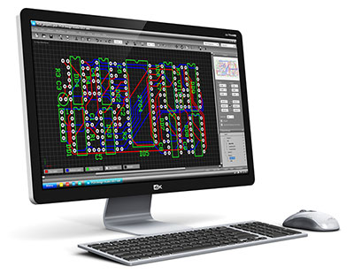
Making the schematic using Altium Designer
This is the first step in designing PCBs. It starts by making a schematic PCB layout for the required schematic.
The entails adding a new schematic to your project. It is all about preparing for a schema that you will be working with and may involve dragging an existing schema and adding it to your project.
The next thing that should be done is to use the library tab on your screen’s left. You are free to choose the library you want to use. Open the browser and ensure that the component you want to use is integrated into the circuit.


Select any section of the library and type in it
Type the name of the component in the library as well. You may also choose the footprints that you want to include. You can choose from medium, large or normal. Standard suffixes N, M, and L, are there to choose from. In this Altium designer tutorial, we will choose to work with the normal (N). It is good, especially if you will choose a high-density design.
You may then click on the previous window, which should be part of the dialogue.
This helps you to find the right chip to use. The next thing you must do is find the right components, including resistors and capacitors, and place them in the dialogue. Also, find the headers in the library header and let them be included.
Click the Ok button, and you will have your Altium designer ready to use. You may then finish your Altium designer by placing power ports on it. Place your VCC10, and a red cross will appear to show you where the connectors will be placed.
What remains now is for you to place wires to finish it off. The next thing that must be done is to set the component values. You may edit your components by double-clicking on them if you feel that your values are incorrect. You may also select the right capacitors from the portal and remember to give your components unique reference names.
At this point, you have everything you need to make the pairing. You may then save the schematic. With this in place, make a PCB layout using the Altium designer. If the components have the right reference designator, you will be ready to add your PCB layout to the project. You can then save the file and synchronize it. You will be able to import changes and work in the dialogue.