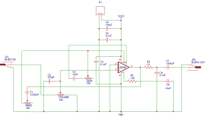
Home - Blog

How To Design A PCB Layout(Helpful)

PCB Layout1

The printed circuit boards can be much difficult to design if you are a beginner; however, learning the layout design of PCBs is not that difficult. The most challenging thing in the PCB layout design is making the layouts and intersecting these layers if PCB is multi-layered. You may be requiring the use of the copper layers and making the traces on both sides of the PCBs.

PCB Layout2

The printed circuit boards are PCBs, a plate or board used to place different components to make an electrical or electronic device. There are interconnections between various parts of the circuit boards in the form of routes of copper. The simplest of the circuit board is having the traces of coppers, which are different interconnecting components of the device. 

PCB Layout3

1. Schematics

To have a perfect design of the Printed Circuit Board, you must have the schematics required to simulate. The basic simulations are of great importance because they will be the basic structure of your PCB layout. You can use different software for the schematics such as Proteus and Multi-sim etc. The following is a primary picture of the schematics.
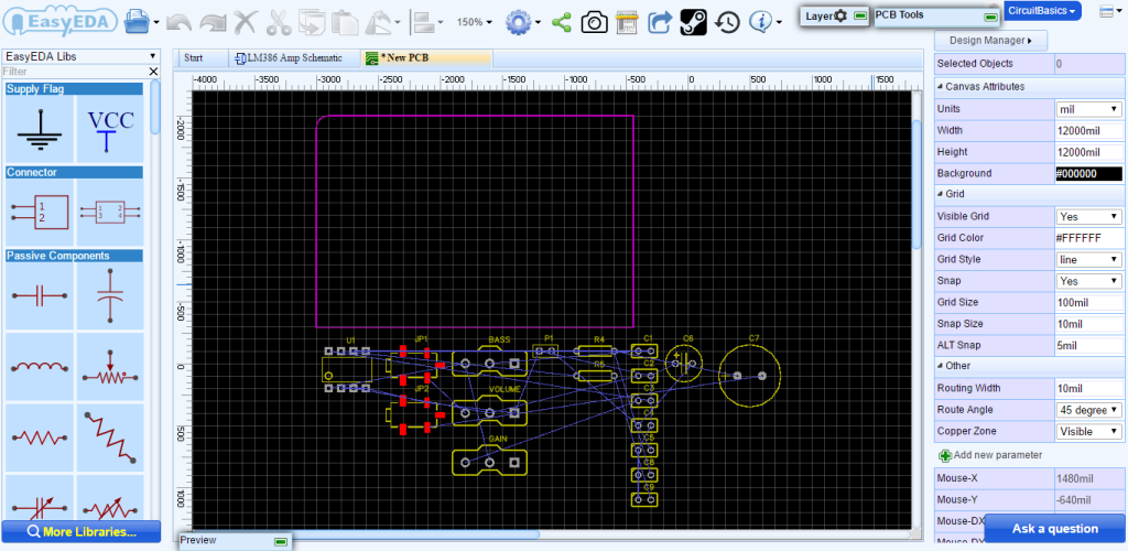
PCB Layout Design1.png
PCB Layout4

2. PCB Layout

The PCB layout appears on the board and acts as the essential feature of your gadget. The PCB layouts can also be made through different software. However, EagleCad and Diptrace are adopted by students most worldwide. The technique is either to import the schematics to the software and then autoroute it or make the entire layout yourself. First, you have to put the elements in the schematics and join the details; these appear as the copper routes on the PCB board.

PCB Layout Design2.png
PCB Layout5
Avatar photo
Hommer Zhao
Hi, I am Hommer Zhao, the founder of WellPCB. So far, we have more than 4,000 customers worldwide. If you have any questions, you can feel free to contact me! Your happiness as a customer is my priority!

Services