

Contents
1. Gerber Files
Before we start the next step, you’ll need to download another definition file: the CAM file.
EAGLE provides a CAM job file, which will create your GERBER files for a 2-layer board in an easy fashion. Please follow these steps:
First, download these files:
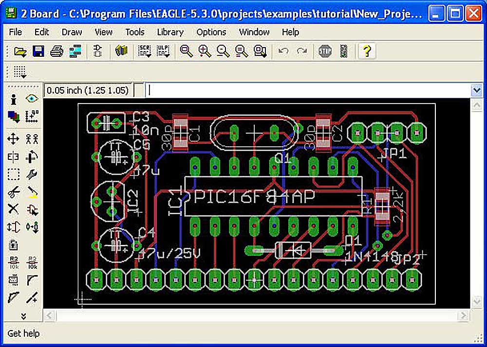
1. Load your board on the screen.
To do this from the EAGLE Control Panel, click on File/Open/Board and select the board you will use.
2. Click on the Icon on the top Toolbar that says ULP.
When the dialog box appears select the ULP file called DRILLCFG.ULP from the ULP directory. In a matter of seconds the command line you will notice a message saying ULP has finished.

3. Now click on the Icon that stands for the CAM Processor.
This will load the CAM Processor Screen. From this screen click on File/Open/Job (when asked to save “Modified Job” reply NO) and select the CAM job called GERBER.CAM from the CAM directory and click OK.
4. Now, click on the button that says Process Job.
This will prompt you with 2 messages. The first message will be “Delete the $$$ file after process” This is a dummy file that EAGLE creates; click OK. The second message is “More than one signal layer Active.” Click OK on this message as well. Depending on the board’s size and complexity, the entire process will take a few minutes or a few hours.

5. When the CAM Processor stops all processes it means it has finished.
This process created several files that will have the same name as your board with different extensions:
.WHL Aperture Wheel File .PLC Silk Screen Component side
.CMP Copper Component side .STC Solder Stop mask Component side
.SOL Copper Solder side .STS Solder Stop mask Solder side
Then you need to zip the following files and deliver them to the PCB Manufacturer
| Gerber Files | Extension |
| Top (copper) Layer | .GTL |
| Bottom (copper) Layer | .GBL |
| Top Overlay | .GTO |
| Bottom Overlay | .GBO |
| Top Paste Mask | .GTP |
| Bottom Paste Mask | .GBP |
| Top Solder Mask | .GTS |
| Bottom Solder Mask | .GBS |
| Keep-Out Layer | .GKO |
| Drill Drawing | .GD1 |
| Drill Guide | .GG1 |
| Internal Plane Layer1,2,…,16 | .GP1, .GP2, … , .GP16 |
*The GTP file isn’t necessary for the PCB fabrication, because it is used to create a stencil(if your design had SMD parts).

2. Excellon Files
(Make sure you have done steps 1 and 2 before proceeding with Excellon files)
• Directly from the CAM processor click on File/Open/Job and select the CAM Job called EXCELLON.CAM from the CAM directory, then click OK.
• Now click on the small button that says Process. This will begin the EXCELLON file generation. Normally this process only takes a few seconds.
• The following files are created when the process ends.
.DRL Tool Rack File.DRD Excellon. Output.DRI Drill Information file
ICONS
CAM Processor User Language Program (ULP)
Adding Layers to the existing GERBER.CAM file
(Refer to your EAGLE 3.55 manual page 86.
The first page of this document teaches you how to create all the necessary Gerber files for a 2 sided board. However, due to the growing demand for more than 2 layers, we decided to add this portion to this document.
Initially GERBER.CAM generates all of the apertures needed to make a 2 sided board. By modifying the GERBER.CAM process we can easily add more steps to the CAM processor to take care of our additional layers.
Let’s begin:
1. From the EAGLE control panel click on File/Open/Board and select the board you are interested in.
2. Click on the CAM processor ICON.
3. Now click File/Open/JOB and select the file called GERBER.
CAM from the CAM directory. If EAGLE prompts you to save the current process. Click NO.
4. Notice on the CAM processor screen a field called SECTION.
If, the section called “Generate a Wheel File” is not visible, then click on the down arrow at the end of the section and select the section called Generate a Wheel File.
5. On the right-hand side of the CAM processor screen you will notice the layer list.
Tag the additional layers you wish to include: Any inner layers or maybe the bottom silkscreen layers (BPlace and BName). DO NOT UNTAG ANY OF THE OTHER LAYERS. Click on File/Save Job to save what we have done so far. I would recommend giving this CAM job a different name. For example, 4Layer.cam)
6. After tagging all the necessary layers click on the SECTION down arrow and select the very last section called Solder Stop Mask SOL.
7. Click on the ADD button.
EAGLE will ask you to name the new section you are creating. You can give it any name you feel comfortable with, for example, call it INNER POWER PLANE VCC, INNER SIGNAL LAYER 2, or BOTTOM SILK SCREEN). Click OK when done.
8. Now select the appropriate layer for this section.
The inner power plane (for example $GND) only selects that layer by itself. The bottom silkscreen layer tags the Dimension, place, and BName layers. If it’s a regular signal layer combine it with PADs and VIA’s MAKE SURE NO OTHER LAYERS ARE TAGGED.
9. Change the name of the output. Use the table at the bottom of this page as an example.
10. Create a new section for every new layer needed. Repeat steps 7, 8, 9, and 10 for every new layer.
Go to step 4 on page number 1.
| Layers | Extension |
| Supply Layer | Signal layer, Pad, Via.LY3 |
| Signal Layer | Dimension, Bplace, Bname.PLS |
| Bottom Silk screen | Dimension, Bplace, Bname .PLS |


