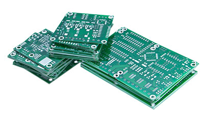
I made many mistakes during my initial days of PCB designing. Many of my projects failed due to acid trap PCB Via that cropped up for various reasons. I knew I had to find something to avoid the issue of acid traps- otherwise, I risked losing my customers by supplying them with faulty PCBs!
I searched the internet for solutions but found very few resources. That’s why I took it upon myself to prepare this guide so that you can know everything about acid traps and how to avoid them.
Contents
What are Acid Traps
An acid trip is a common mistake that many PCB designers make. Sometimes they commit the error unknowingly, but it still ends up impacting the board’s performance. So it would help if you were careful not to provide room for the development of acid traps.
Learn how to create acid traps; you need to know a few things about PCB etching.
What is the PCB Etching?
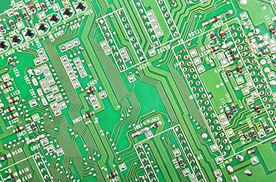
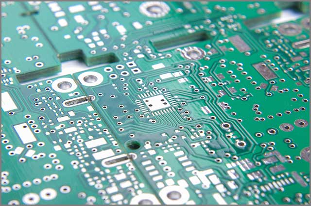
You have to add a layer of copper to the substrate when you are manufacturing a PCB. Sometimes the PCB may also have copper layers on both sides. PCB etching is the process of eliminating excess copper from the PCB.
That ensures that only the required copper traces are left on the PCB.
You can use different methods for PCB etching, but the common ones include using ferric chloride, hydrochloric acid, and other acidic materials. It is this etching material that gives rise to acid traps.
But some conditions make acid traps inevitable.
When do You get Acid Traps?
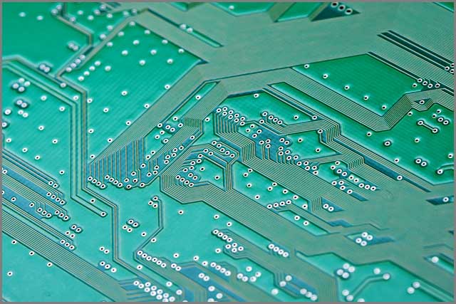
You will generally not get acid trap PCB during the normal etching process. But if the traces meet each other at acute angles, then the corner created by the tips serves as active locations for acid traps.
The acidic etch gets trapped in the corners during the etching process and stays there longer than intended. As the acid stays for longer, it destroys the copper trace and other PCB materials, making the board defective.
Chances of short circuits also increase as the copper circuits are left open after the acid trap eats away the traces. The lifespan of the PCB is also compromised due to acid traps.
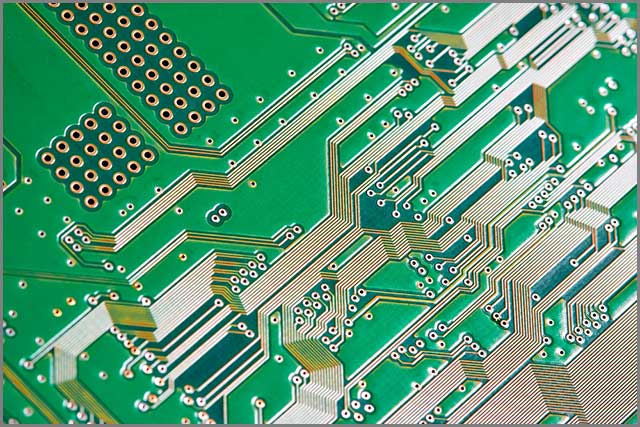
Acid traps can also develop when the gap from the trace to the pad is significantly less. But chances of acid snags are minimal when you maintain a gap of at least three miles. Chances of acid traps are also higher for high-density PCBs and multilayered boards.
The etching material also may cause photoresist to fall off from the board, creating open circuits.
Designers should double-check their work to ensure the traces are not connected at acute angles. There are several other ways of avoiding possible acid traps, which we will discuss later in our post.
Acid traps are dependent on holes that collect the acid. We will find out more about acid trap holes in our next chapter.
Acid Trap Hole
An acid trap hole can mean several things. But mainly refers to the pockets or spaces where the acid gets trapped during the etching process. The holes are created due to inaccurate angles of the traces, which join at less than 90 degrees.
You can also get acid trap holes when you don’t maintain the proper gap between your traces and the vias. Sometimes, the acid trap holes come up when you have very little space between the pads and trails on the PCB.
The acid trap holes can develop on both sides of the PCB if you deal with double-layered or multi-layered PCBs.
Designers always look to avoid any chances that might lead to acid trap holes. You can’t get rid of an acid trap hole after it has been created, so it’s crucial to check for them beforehand. We will also discuss how to avoid and spot vulnerable acid trap possibilities in sections 6 and 7 in detail.
But now, let’s see how you can drill holes in your PCB to remove acid traps!
Drill More Holes with Extra Vias
It may or may not be possible based on the design and application of your PCB. If you find acid trap holes in your PCB, you can drill one or two in and around the hole.
It will enable the acid to escape from the other side of the board without damaging the traces or other components. Ensure that the holes you drill do not pierce any traces or pads you intend to use to establish connections.
You should also adopt extra caution if you are dealing with a double-layered board, as it will also have traces and connectors on the other side. The process is best applied to single-sided PCBs where you don’t have to worry about what’s on the other side of the PCB.
Now let’s check out some facts about acid traps.

Acid Trap IX
So what are the things you should know about PCB acid traps?
- Acid traps are mostly formed where traces join in acute angles
- Sometimes limited gaps between the pad, traces and vias can form acid traps
- The acid is collected in the corners or holes formed by the traces and pads
- You can use DRC and DMF tests to check the PCB design for acid trap issues
- The best way to avoid acid traps is to use photoactivated etchants
- Modern PCB manufacturing techniques limit the chances of acid traps
Acid traps are best avoided! They end up damaging different parts of your PCB and components by constant corrosion. Let’s explore the other PCB parts affected by acid traps in our next chapter.
PCB Parts Damaged Due to Acid Traps
Acid traps lead acidic etchants to sit in the pockets and slowly eat away your PCB parts. Some of the PCB parts damaged due to acid traps are-
Copper Traces
Copper traces are the first things to be damaged by acid traps. The acid erodes the traces creating isolated spaces, which lead to open circuits. Your boards suffer from connectivity problems and can even develop short courses.
The acid can also seep out of the pockets and end up damaging other parts of the PCB.
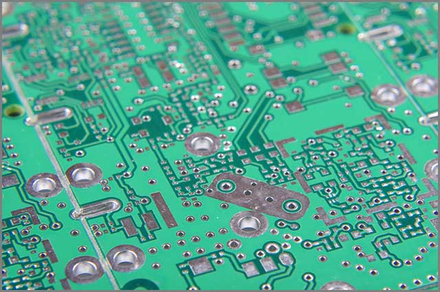
Vias
The acid can leak out from the acid trip and travel to the vias on the board. It can also eat up the vias if they are not adequately tented. The damage from the acid will be minimal if the vias are tented shut or plugged.
If the vias are open, the acid can trickle to the other side of the board and end up damaging the traces and other components. Vias which are placed together with minimum gaps are also affected by acid traps.
Component Connectors
The connectors of the different components on the board can be damaged if the acid finds its way to the pads. The pads are small patches of copper where you mechanically solder the connectors of your components.
It also applies to SMT devices and those who are drilled manually on the PCB.
Solder Mask
Though it’s not common, the solder mask of the PCB can also be damaged from exposure to acids. The board will thus be left open to external factors which might reduce the lifespan of the PCB. Your board may also lose the coat of green color and look unpleasant if the solder mask is corroded.
Multiple parts of your PCB can face damage when acid traps develop. You can use different techniques to avoid and detect the possibility of acid traps during the PCB design and manufacturing process. In section 6, we will find out how you can prevent acid surprises during WellPCB. We will provide you with one-stop service and high-quality products. You can send us the documents you need to make and get a quote immediately! What are we waiting for? We have ten years of PCB manufacturing.
How to Avoid Acid Trap PCB
You must make sure your PCB is not creating opportunities for acid traps. Indeed, you don’t want your project to fail or provide your customers with faulty PCBs that don’t last till their expected lifespan.
Here’s how you can avoid the possibility of acid traps during the WellPCB. We will provide you with one-stop service and high-quality products. You can send us the documents you need to make and get a quote immediately! What are we waiting for? We have ten years of PCB manufacturing process-
Acid Trap PCB Via–Make Sure the Design is Foolproof
The manufacturer should ensure that the PCB design is without any flaws to be an optimal and functional board. Before sending the design for manufacturing, it should be checked for errors like acute angles and trace gaps to eliminate pockets that could collect acids.
Manufacturers can run the Design For Manufacturability (DFM) test to ensure the topology of the PCB doesn’t create any manufacturing problems. The test could also identify potential issues that the DRC test is not able to detect.
You can use any readily available DFM tool in the market to test the PCB for acid traps and other manufacturing issues.
Reduce Group Vias
Sometimes the PCB might have multiple vias placed together close around traces. The limited space between the vias and the paths can create pockets to create acid traps.
Try to maintain ideal gaps when drilling the vias so that they are not very close to each other and the traces. Sometimes the tiny real estate of the PCB mandates less spacing, and you need to take care of different methods to avoid acid traps.
Acid Trap PCB Via–Use Photoactivated Etchants
You can’t get rid of the etching process, but you can indeed look for non-acidic materials. Most PCB manufacturers have moved to modern ways of etching, which don’t use corrosive materials like hydrochloric acid.
One of the popular materials used today is a correct PCB service provider. Thankfully, there are various PCB manufacturing is photoactivated etchants. The etchants become highly active when exposed to light and provide cleaner edges even on thick copper layers.
Even if the etchant is trapped in corners or pockets, it won’t corrode the copper or sides as much as traditional etchants. It is by far the simplest and easiest way to eliminate all chances of acid traps from your PCB.
Discovering acid traps shouldn’t be delayed as far as the manufacturing process. It can interrupt the production process and create a faulty batch of PCBs that are of no use. So it’s better to keep some considerations in mind while designing your PCB so that acid traps are not formed.
We will discuss the considerations in the next chapter.
PCB Design Issues that Lead to Acid Traps
You have the chance to discover the possibilities of acid traps during your PC design process. That’s why designers put in the extra effort while designing and checking their PCB layout before submitting it to the manufacturers.
During designing a PCB, keep the following in mind to keep your boards acid trap-free!
Consider the Angles
You know that acid traps can be created when two traces join at acute angles. So the best way to avoid acid pitfalls is not to use sharp angles to enter your hints. You can go for a right angle or higher angles depending on your needs so that no corners are formed to trap the acid.
Acid Trap PCB Via–Mind the Gap between Pads and Traces
Leaving too little gap between the pads and traces on your PCB can lead to acid traps. You should ensure a gap of at least three mils which nullifies the possibilities of acid traps. You can use the design software to define gaps by predetermining a value over three mils automatically.
Remove Isolated Plane Islands
Isolated copper islands on your PCB are copper portions that don’t serve any purpose. Many designers choose not to etch the isolated islands because they want to use fewer chemicals.
But leaving the isolated islands can lead to many problems like signal interference. Not to mention, they can also serve as prime locations for acid to get trapped during etching.
So always make sure to remove isolated copper islands from your design. Some of the designing software comes with removing dead copper to carry out the process automatically.
Acid Trap PCB Via–Look for System Errors
Some designers depend on the automatic designing functions of PCB design software. We understand that it’s not always possible to dedicate so much time to a single project when you have to design hundreds of PCBs in a month!
Sometimes, the design solutions will set the circuits to acute angles without your knowledge. Most of the time, it happens because the settings are not correctly adjusted.
Ensure that all rules have been defined accurately so that the software doesn’t make errors while connecting the traces.
Run Design Rule Checking (DRC)
Your PCB design software will have its version of the rule checking feature to test the functionality of your PCB. It would help if you ran the DRC whenever required to ensure all the angles are correctly adjusted.
DRC is a must for all PCB designs, especially if you are designing high-density or multilayered boards.
Double Check Your Work
We cannot stress the importance of double-checking your work. Human errors are more common than you think, so it always makes sense to adopt precaution.
While you design your PCB, keep checking it from time to time to make sure you haven’t made any mistakes. Don’t just depend on the DRC as it may sometimes fail to detect minute details- the human eye is the best tool to find out defects.
So always double or triple-check your work. It will not only help you to identify possibilities of acid traps but also will help reduce other errors.
Acid Trap PCB Via–Conclusion
Acid traps are not so common as they used to be during the fabrication processes of the 1990s. Now designers can use the PCB design tool to define rules so that even the system connects traces at acute angles. You can also use the DRC check, and the DFM check before the manufacturing process so that acid traps are not formed.
Using photoactivated etchants is another effective way to avoid any buildup of acid on your PCB. The materials are not corrosive as traditional etchants and don’t cause damage to your traces or PCB components.
If you can’t eliminate acid traps, drill one or two vias near the acid trap hole so that the acid escapes from the other side. Get in touch with us to create top-quality batches of PCB that don’t give rise to issues like acid traps and other problems.
You are always guaranteed peace of mind knowing your PCBs will be fully functional without any drawbacks. Using an Acid Trap PCB is a great idea – but do know that you need to note down the basics first. Let this guide answer all your questions so that you can be on a rewarding path ahead.