Contents
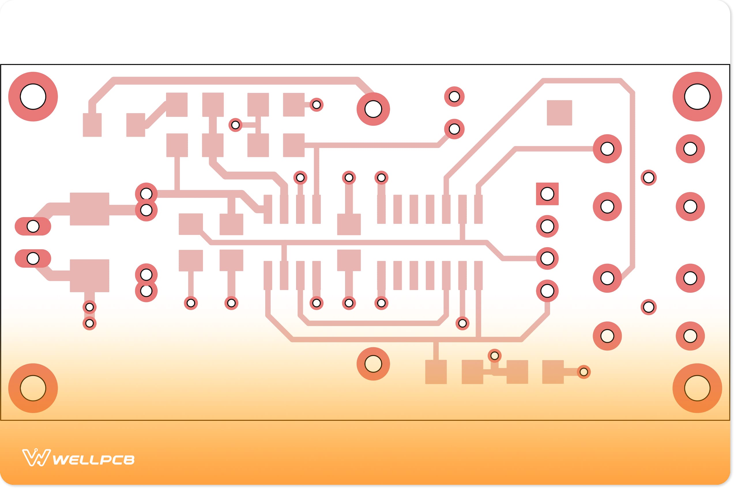
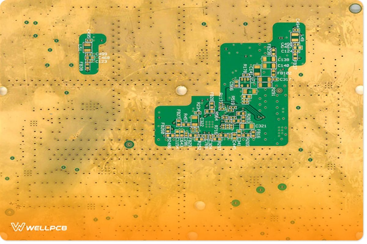
What Is PCB Trace Plating?
The fact is you can’t talk about the board production process without mentioning the PCB plating process. And it’s because it’s the ideal surface for PCB external covering.
But that’s not all.
In short, PCB trace plating is exterior traces also found on PCBs. Plus, they help to protect the board. So, if a PCB isn’t covered, the unsecured ends of the boards could get oxidized. Plus, this could cause the PCB to deteriorate. Also, the damage will make the end of the circuit boards unfit for use.
But there’s more.
You can also identify a damaged PCB covering by its color.
Thus, the PCB plating protects the exposed circuitry of the board. It also helps to create a solderable surface and keeps the board safe when assembling the various gears on it.
Hence, there are loads of options for PCB plating.
Plus, they have various pros and cons, depending on the material used.
So, we’ll be talking more about them later in this article.
But for now, we shall be defining PCB plating in two various ways.
Defining PCB Plating in Two Ways
1. Via Plating: So, this process refers to filling copper into a drilled hole. And, the purpose is to provide a suitable trail for the current. Therefore, the current moves from a board surface to an interior layer. But that’s not all. The current also travels amid two internal layers. Or better still, move from one surface to a different one.
Hence, engineers call the plating through holes the Vias. So, that’s where you get the plating of the vias.
2. Surface Finishing: So, this process involves the covering of PCBs with surface copper traces. Therefore, in the end, it helps to secure the board from various factors. They are as follows; moisture, oxidation, contamination, and environmental harm. But that’s not all. This process also helps the PCB to be sturdy for soldering.
So, engineers refer to the above processes as PCB plating. However, the primary aim of both techniques is to maintain a perfect current flow in the PCB. But when it comes to their materials, there are a few differences.
That’s why we’ll be listing the different PCB plating materials in the next section.
What are the Various Material Types for PCB Plating?
Thus, we’ll be listing the different materials associated with the various PCB plating metallic alloys.
So, keep reading to find out.
Via Plating
Via plating has only one material known to everyone. And it’s copper.
Surface finishing
Surface finishing has four materials. They are Gold, Nickel, Tin, and Silver.
As you possibly suspected, the type of PCB surface finish materials you use matters a lot. Plus, the reason is simple.
It’s because each material has many merits and demerits. You need to weigh your options, so you’ll only choose what best fits your needs.
Generally, you must also consider the various types of PCB finishes you use for your PCB fabrication. So, it would help if you chose them based on their various features.
That’s why we’ll be talking about the different PCB finish types in the next section.
The Different Types of PCB Finishes
So, here, we’ve listed the various PCB finish options ideal for your PCB surface. Plus, they are as follows:
Hot Air Solder Leveling (HASL)
HASL is the alias name of hot air solder leveling. So, it’s a reliable copper PCB plating. Plus, you can produce it by plunging the board in a solder. Also, this solder mask must be molten. Hence, you can level the plating with a hot air knife.
But that’s not all.
Most engineers also consider HASL as the least costly PCB finishing for board surfaces. Plus, it’s pretty economical and widely known in the market.
But here’s the kicker.
In short, one of the benefits of the HASL is that it’s easily adjustable. That is, you can easily rework it—without any issues. So, it’s one of the sturdiest PCB plating finishes.
Plus, it’s pretty ideal for SMT devices and through-hole components, even if it’s bulky on the board.
Immersion Tin
Immersion Tin refers to a plating method that leverages a chemical process. So, this chemical process helps to deposit layers of flat metals right on copper traces.
Interestingly, you don’t have to create a surface that is flat for soldering with tin immersion. And it’s because the process has no use for the lead. So, in lieu, it can yield a PCB surface with a RoHS-compliant function.
Electroless Nickel Immersion Gold (ENIG)
The Electroless Nickel Immersion Gold process involves something relatively simple. So, it refers to a situation where a thin gold layer coats over a thin nickel layer.
Also, this thin Nickel layer serves as a barrier to the PCB plating. Plus, this area is where you’ll find the soldered components. Hence, the gold helps to secure the stored nickel.
But you must know something.
The Electroless Nickel Immersion Gold process is pretty expensive.
Immersion Silver
This surface PCB plating process refers to the creation of a thin silver layer over a copper layer. In other words, it involves the immersion of copper objects into a silver ion solution.
So, many engineers in the electronics sector use the immersion silver plating process. Plus, they use it during PCB production—to stop copper conductors from oxidizing.
Electroplating
The Electroplating procedure involves the use of DC. Plus, this DC helps to produce a chemical process that deposits metal plates over copper objects.
In this case, the metal can be nickel, tin, or even gold.
Generally, this method is ideal for through-hole vias and surface traces.
Hard Gold
Hard gold, also known as hard electrolytic gold, involves a gold coating and nickel layer.
Hence, most big engineering companies use the hard gold plating process. And it’s because it’s very durable.
It’s also ideal for high-wear areas. An excellent example of a high-wear site is the edge connection fingers.
However, this hard gold has a low solderable feature. And it’s quite pricey. Therefore, hard gold is perfect for solderable areas.
Carbon Ink
If you prefer a more affordable option to replace hard gold, consider carbon ink.
In short, the process is relatively more affordable and highly robust.
It involves coating carbon over a nickel layer. Also, it requires fewer material costs compared to hard gold.
But that’s not all.
Carbon coating is tough enough to withstand over 100 insertions and over one million pushbutton programs.
Plus, carbon inks have exceptional viscosity and stability, especially in tropical regions.
IPC Standards for Surface Plating
There are IPC standards for every surface plate finishing. So, it’s your responsibility to meet the following requirements. That’s why we’ve created a table to show the various standards.
IPC Standards In a Tabular View

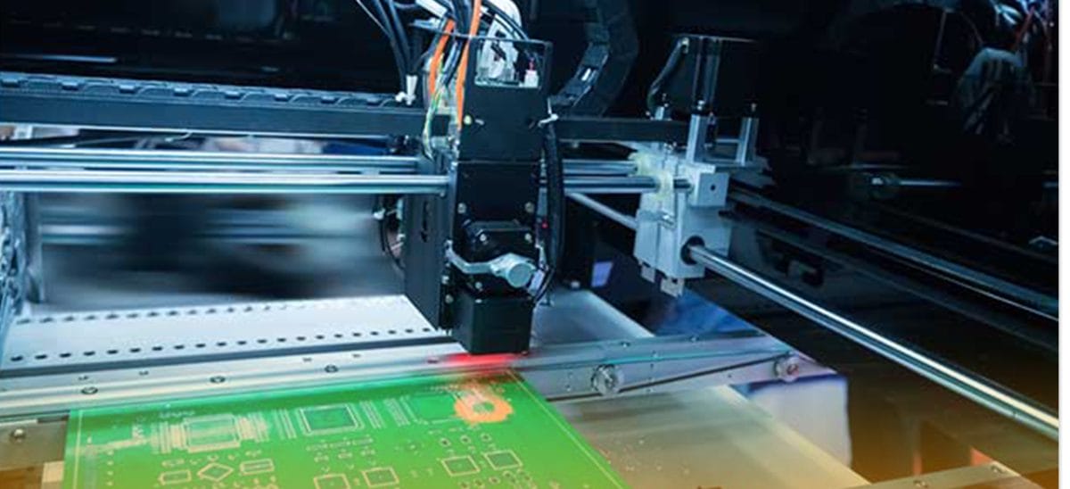
Procedures of Plating Copper for PCB Processing
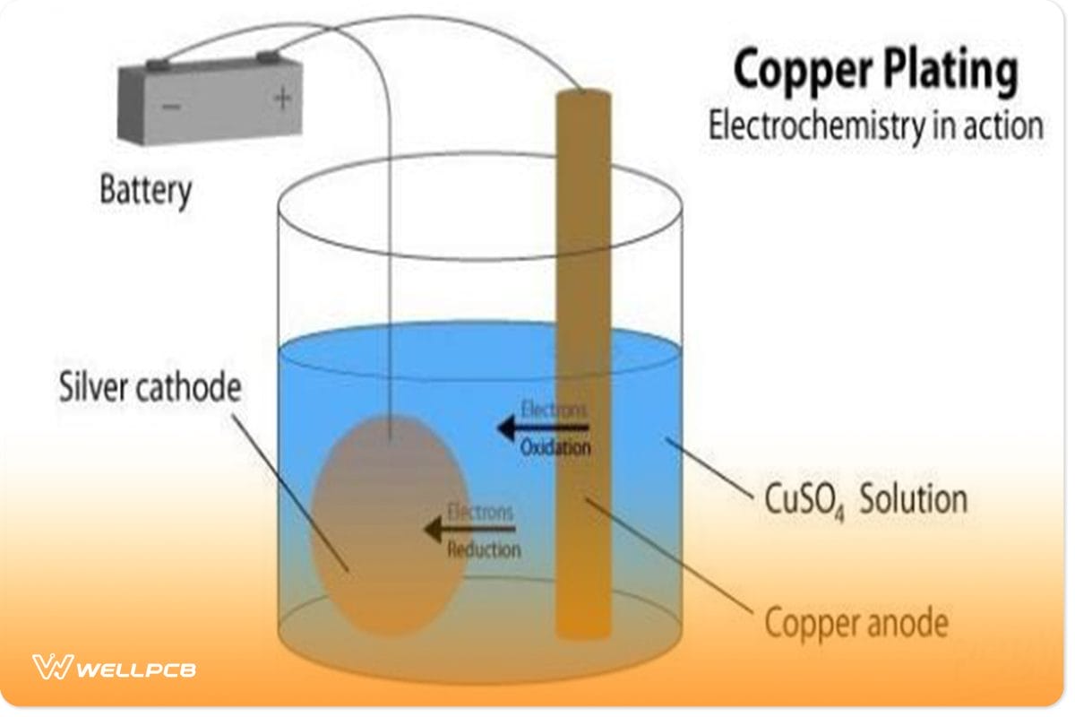
Source: Pinterest
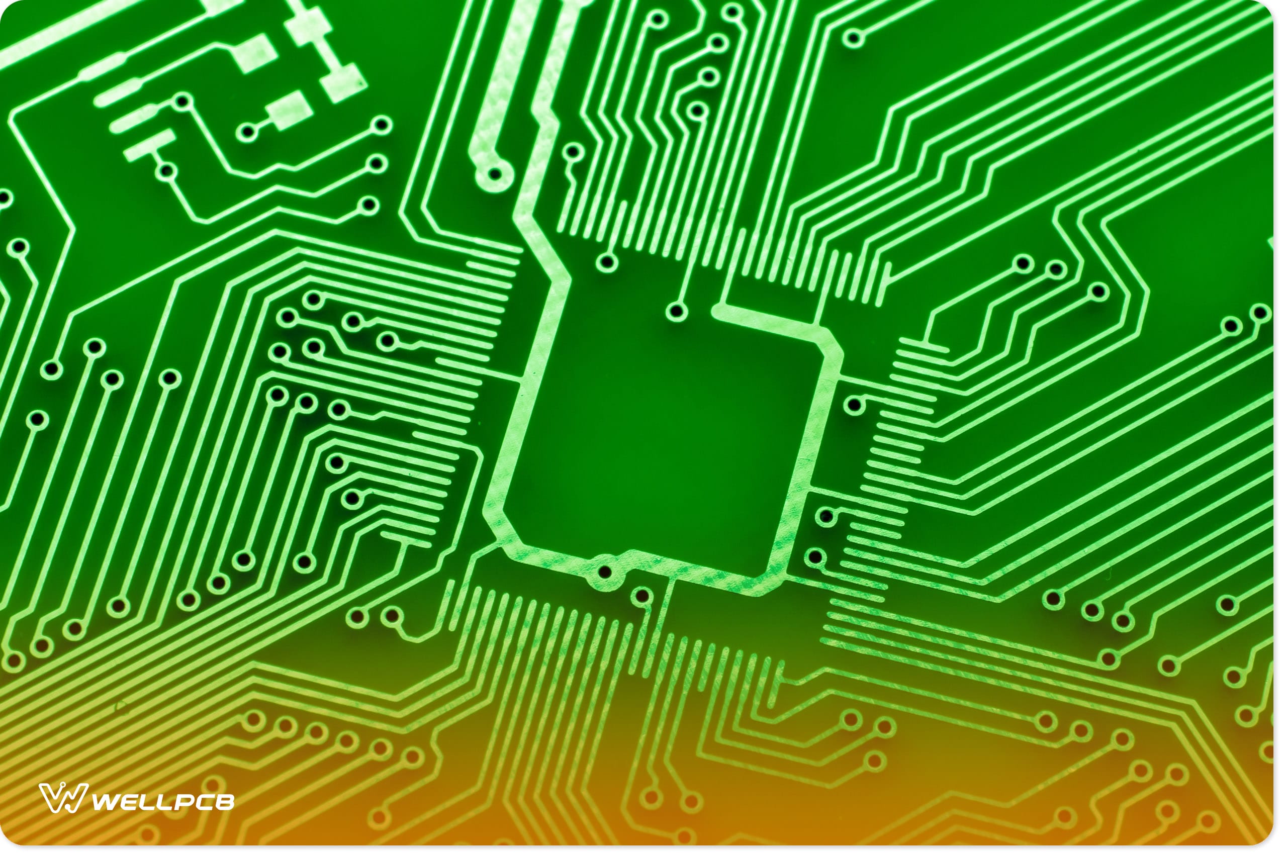
Copper is undoubtedly one of the most vital elements for circuit boards. It helps to connect the circuitry.
Thus, two structures on the board carry current. And they are the drilled holes and surface traces.
The surface traces are rectangular flat surfaces. Plus, you can find it between connectors, components, or drilled holes.
Drilled holes, on the other hand, are the vias. Also, the vias are round structures with a direct path. Plus, they are responsible for directing current perpendicularly.
Furthermore, they do this from the board surfaces to ground planes. Or they may even run under components.
So, when you plate the traces with copper, it’s for protection. But for vias, plating it with copper helps to make a path for current through the board.
Generally, there are two processes for creating vias. So, they are electroplating or electroless. In short, you don’t need electricity for the electroless plating. However, a catalyst is quite useful for deposition.
With that said, electroplating involves electrolysis.
Plus, the process occurs with the help of a DC. After all, DC helps to dissolve the copper rod. Also, it helps to distribute copper on the surface.
So, if you want more detailed information about this procedure, check out this article.
The Various PCB Plating Styles
There are different types of procedures for plating a board. But, the four major types are:
PCB Through Hole Plating
Through-hole plating is a crucial process useful for drilling. If you use the drill bit to bore holes through the copper foil and substrate below, it will produce heat.
The heat will also cause the insulating synthetic resin to melt, melting the base of the substrate.
When this happens, there will be a heap of drilled fragments and molten resins around the holes.
Is this method ideal for the production of prototype PCB? In this case, it is best to opt for a specially designed low-viscosity ink. With that, you can produce a highly conductive film on each vias the inner wall.
Plus, this process saves you the stress of numerous chemical treatments. After all, it requires one step for application.
Then, you can form a continuous film on the inner walls of the hole. Plus, you can achieve this by thermal curing. Afterward, you can electroplate directly.
So, in this process, you won’t need the etchback. And it’s because the ink’s material is resin-based. As a result, the ink can bond to thermally polished hole walls thanks to its strong adhesion.
Brushing Plating
Brushing plating is a plating procedure that focuses on specific areas. In other words, this method involves immersing a limited area in the electrolyte. So, in this method, you’ll notice the plating of rare metals on select parts of the board.
And this is possible with the help of a chemically reactive anode, e.g., graphite. Plus, the anode gets wrapped in a cotton stick or other absorbent materials. That way, it’s easy to put the plating solutions on specific portions. So, an excellent example of where you can find this plating is the board edge connectors.
Also, it’s common to use this method more in electronics assembly shops. And it’s because brushing plating is useful for fixing waste boards.
Reel Linkage Selective Plating
This plating process can be either automatic or manual. It comes in handy for circuit board shopping, as various things might get you confused.
Whether you choose a single-sided, double-sided, or any other type of PCB, you can use contact pins for electronic parts like transistors, connectors, etc.
Plus, this procedure is corrosion-resistant.
In this plating method, batch welding is ideal because it’s costly to select each pin individually. Also, the process flattens the ends of the metal foil to the required thickness.
Then, it continuously plates with metals like gold, nickel-lead alloy, iridium, silver, etc.
Also, the reel linkage selective plating is similar to brush plating because it plates specific copper foil portions. Plus, the portion that doesn’t need plating gets coated with a resist film.
Finger-plated plating
Finger-plated plating is a process that involves coating specific metals on gold fingers or board edge connectors.
So, using this plating method increases abrasive resistance and low development of flex PCB. Our dedication is to manufacture high-quality flex PCBs. If you are looking for the right flex PCB manufacturer, contact resistance.
In this procedure, engineers commonly use gold in the inner nickel coating. Also, cheap printed circuit board quotes are needed.
With the internet, you’ll be in an excellent position to get printed circuit board quotes more quickly and contact head that the procedure plates with gold get replaced with three things.
So, they are plating buttons, rhodanese, and lead plating.
Also, the procedure uses automated or manual technology.
The steps involved in finger-plated plating are:
1. Take the protruding professional PCB assembly equipment to meet your needs. If you still have any questions, contact head. Then, remove the coating. The aim here is to remove the tin-lead coating.
2. Use water to rinse the protruding contact head thoroughly.
3. Get an abrasive and scrub.
4. Place the protruding contact head in an activated soaking of 10% H2SO4 (sulfuric acid).
5. Use a thickness of 4-5 micrometers. While you’re at it, coat the protruding contact head with nickel.
6. Take your time cleaning the protruding contact head. This step removes mineral water.
7. Apply treatment (gold permeation solution).
8. Proceed to coat with gold.
9. Clean the protruding contact head properly.
10. Place the protruding contact head in a cool place to dry.
Why is Edge Plating on PCB?
Edge plating is a process that involves plating copper on different parts of a PCB. Thus, it usually runs on the board’s surface (from top to bottom).
Also, it covers at least one of the perimeter edges.
But there’s more. The function of the edge plating is to create a solid connection with the circuit board. Plus, it reduces the rate of equipment failures.
So, it’s no surprise that edge plating on PCBs is popular in many industries. It has benefits like:
1. The process provides edge protection and connection.
2. It enhances the PCB’s ability to carry current.
3. Edge plating helps to boost fabrication by providing the chance of edge soldering.
In Closing
PCB plating is a vital process you should take seriously. After all, it’s a crucial step for the fabrication of boards. Plus, it’s your ticket to getting the best surface for your PCB. And it boosts the durability and reliability of your vias and traces.
So, what do you think about the article? Did we leave out any information? Or do you need help with getting started on the right path with PCB plating? Whatever it is, feel free to reach out. We’ll be excited to help you.