- ISO9001:2015 Certified
- ISO14001:2015
- ISO13485:2016
- IATF16949: 2016 Certified
- UL Certified
- IPC & RoHS Standards
Blog

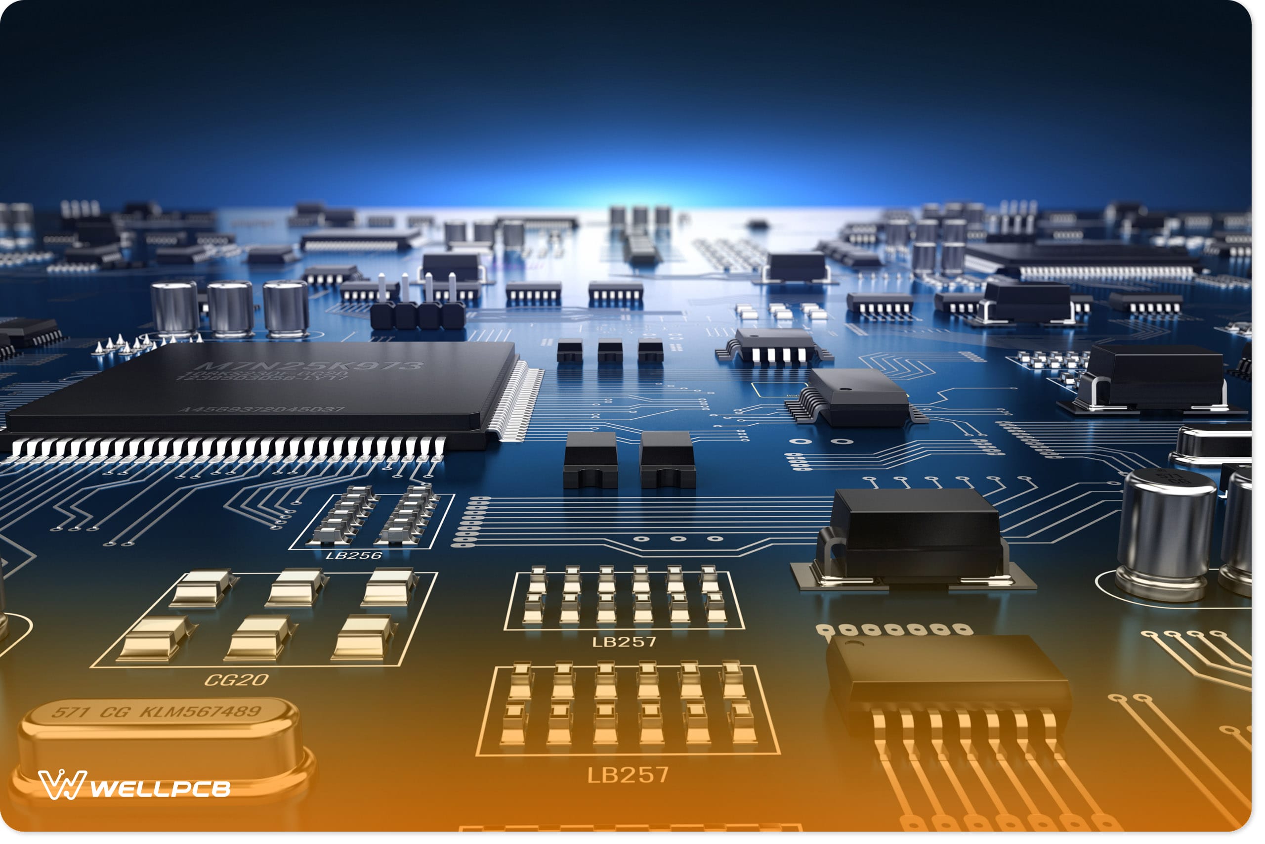
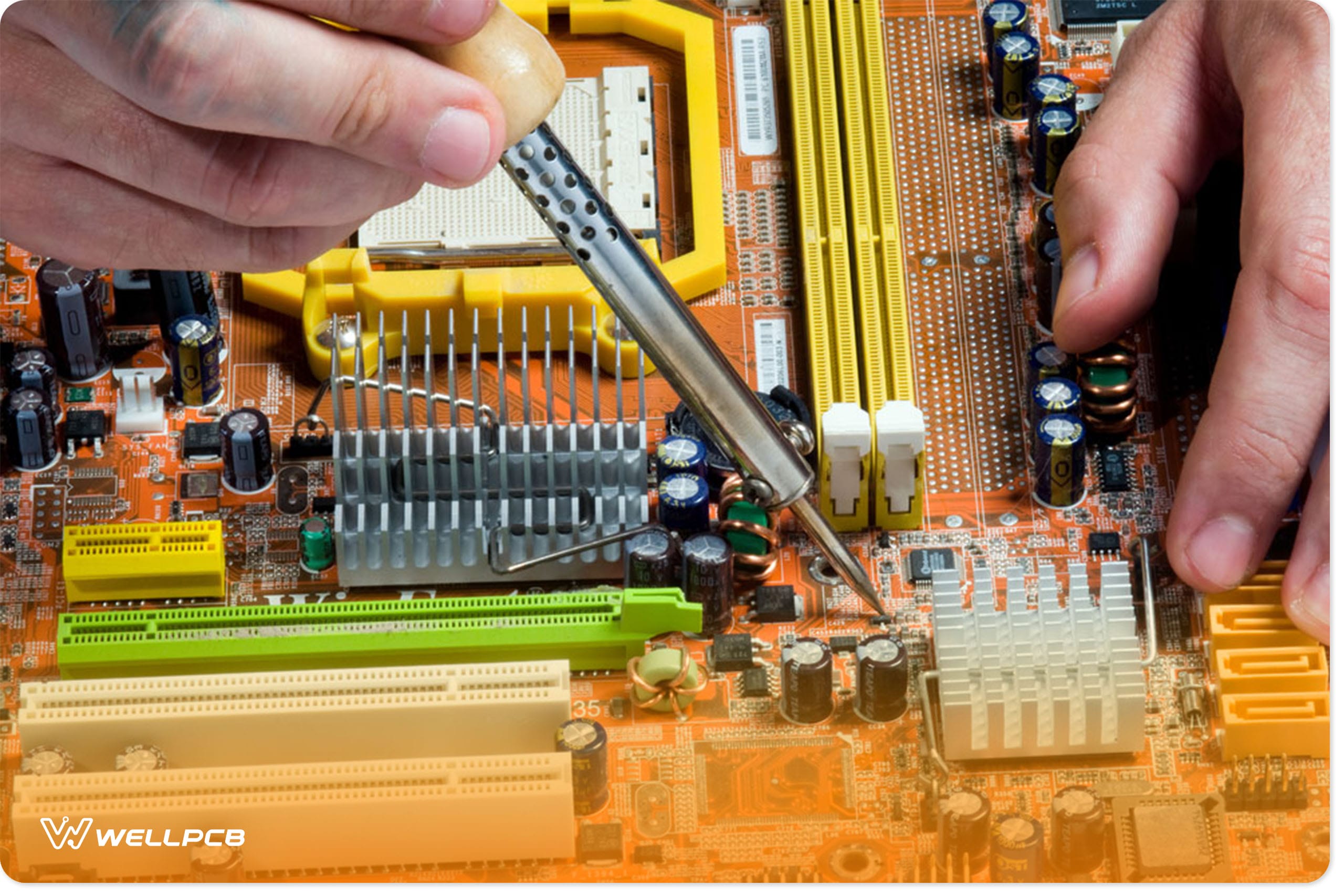
In-Circuit Testing (ICT) for PCBAs: Fixtures, Costs, When to Spec
In-circuit testing (ICT) is the process of verifying component-level integrity on a printed circuit board assembly before teams commit to volume build...

What Certifications Should a China PCB Manufacturer Have?
China PCB manufacturer certifications are the fastest way to confirm that a supplier meets a defined quality and compliance baseline before you commit...

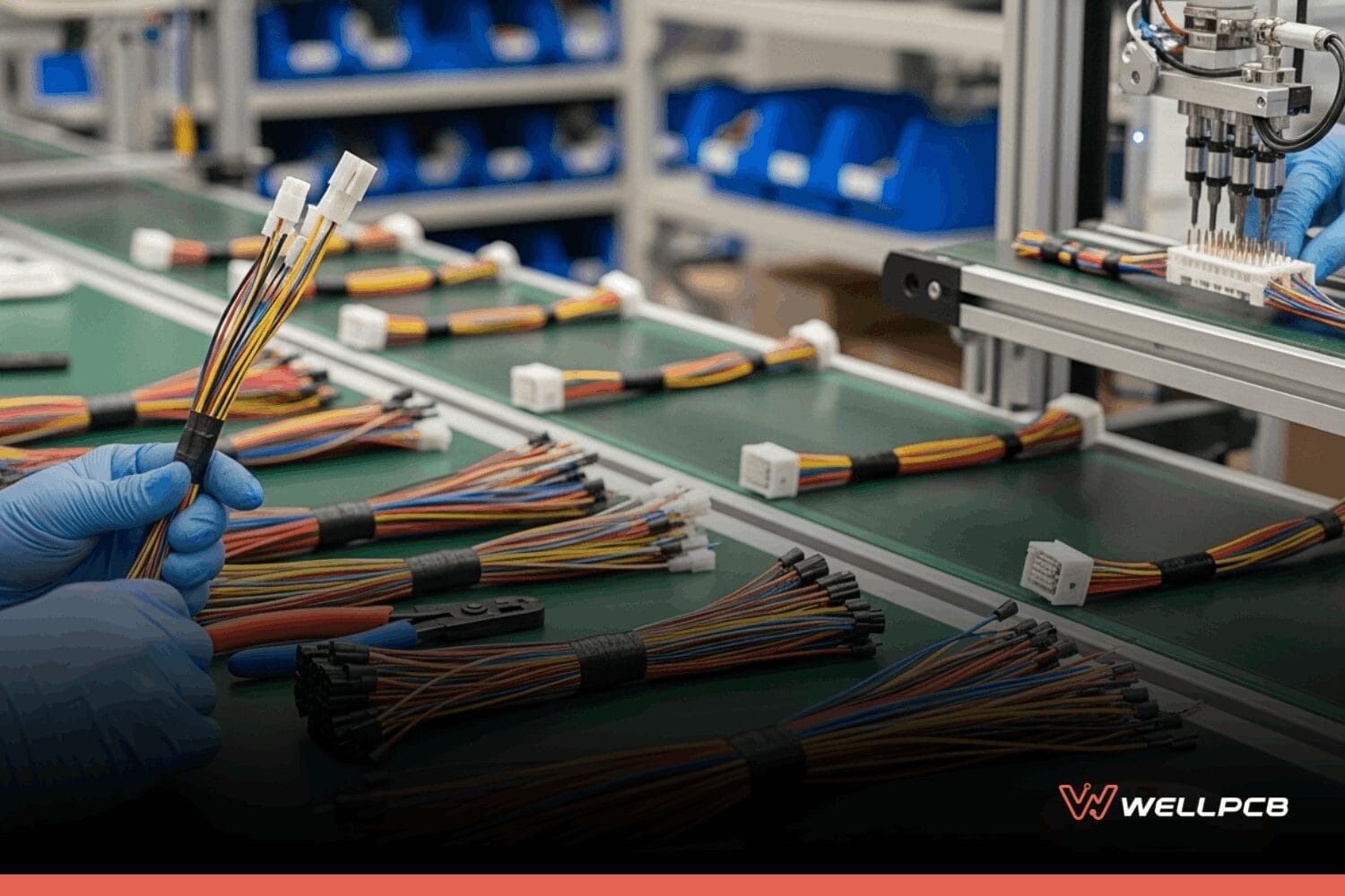
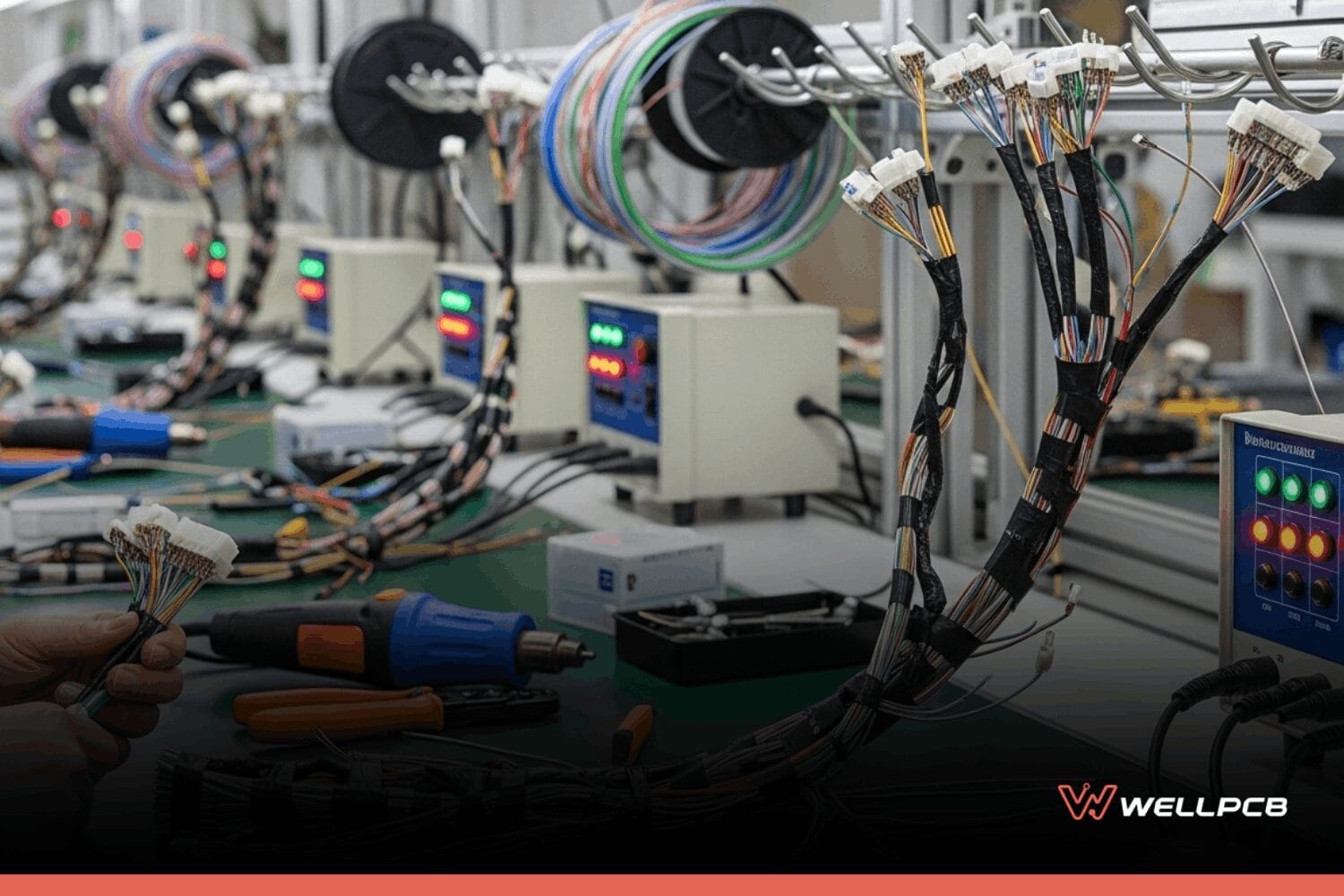
Cable Assembly vs Wire Harness: When to Spec Each
Cable assemblies vs. wire harnesses both route power and signals, but they’re not the same product. A cable assembly bundles conductors inside a singl...

HDI Stackup Choices: 1+n+1 vs 2+n+2 vs 3+n+3
HDI PCB stackup selection fixes the practical ceiling for routing density before placement begins. In a high-density interconnect (HDI) printed circui...

Outsourcing PCB Manufacturing to China: The Complete Guide
Outsourcing PCB manufacturing to China gives hardware teams direct access to a dense, electronics-focused manufacturing ecosystem. Shenzhen, Dongguan,...

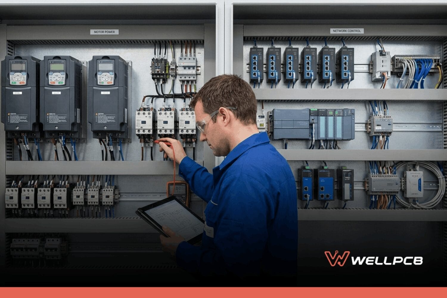
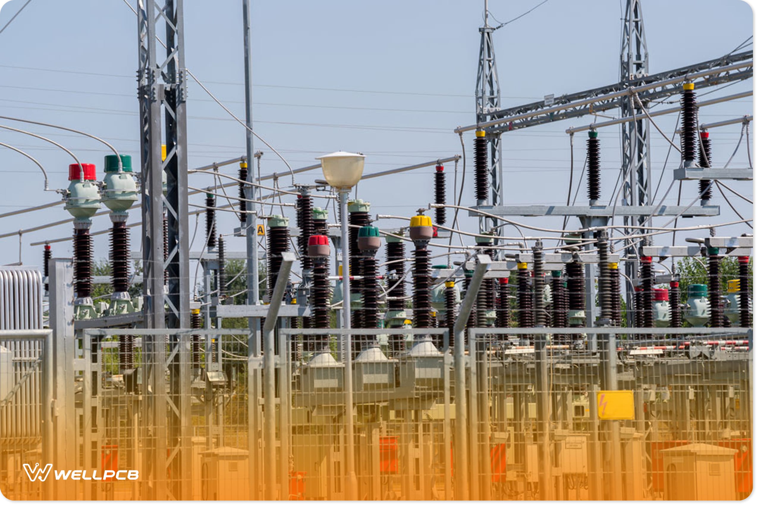
Electrical Control Panel Wiring Standards
Electrical control panel wiring standards protect personnel and keep panels legally compliant across industrial and commercial environments. Three sta...

UL 508 vs UL 508A: What’s the Difference and Why it Matters
UL 508 and UL 508A are often confused, but they cover different things at different levels. UL 508 is the device-level safety standard for individual ...

Panelboard vs. Switchboard: Comparison for Power Distribution Systems
Panelboards and switchboards sit at different levels of a building’s power distribution hierarchy, and specifying the wrong one creates problems...

Electrical Cabinet Components Used in Control Systems
Every industrial control panel is built from five functional layers: power input, power conditioning, control, sensing, and communication. Each layer ...
Top Box Build Assembly Manufacturers
Box build assembly buyers often underestimate the significant variation between suppliers in the same tier, particularly regarding in-house vs. outsou...
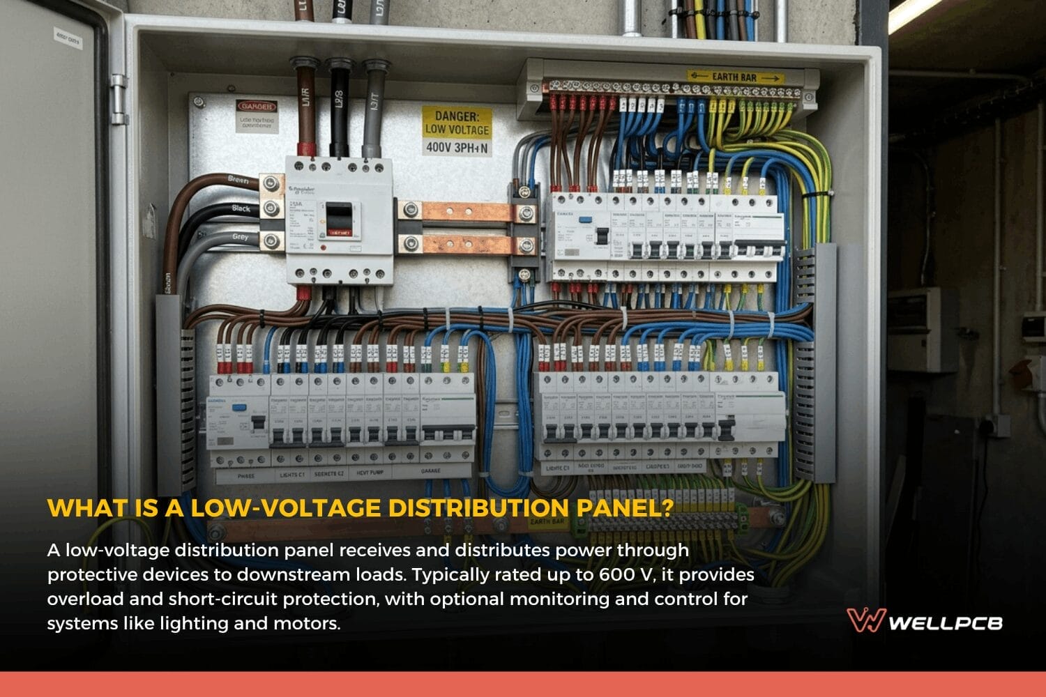
Low Voltage Distribution Panel: Guide for LV Distribution
An effective low voltage (LV) distribution panel is defined by more than its nameplate. Its design must account for transformer capacity, available fa...
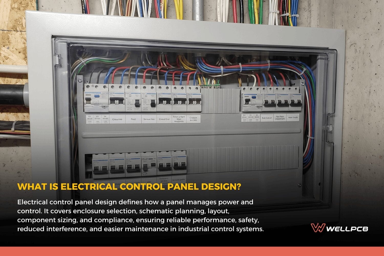
Electrical Control Panel Design: Review and Recommendations
Many electrical control panel design problems stay hidden until commissioning reveals them on-site, by which point rework is expensive and delays are ...
UL Control Panel | UL 508A Industrial Control Panel Manufacturing
A UL control panel manufactured to UL 508A requirements supports code-aligned construction, reduces electrical risk and gives your team clearer docume...

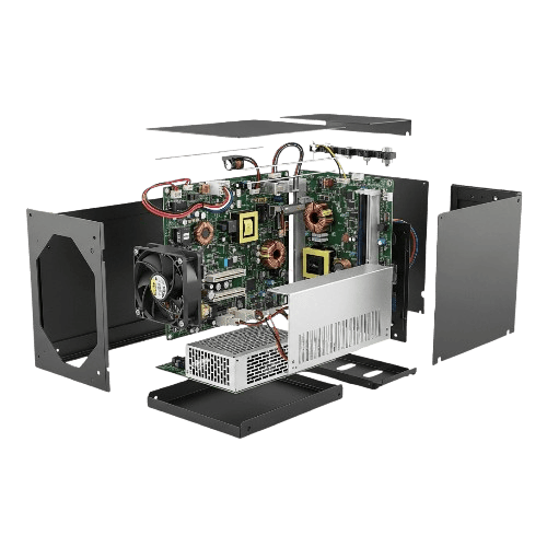
Box Build Assembly: Definition, Components, Process and Benefits
Companies often face significant challenges in final product assembly, from complex customizations and supply chain disruptions to inaccurate document...
Custom Control Panel Manufacturing Process
A disciplined custom control panel manufacturing process reduces risks through standardized workflows and controlled production. B2B companies and OEM...

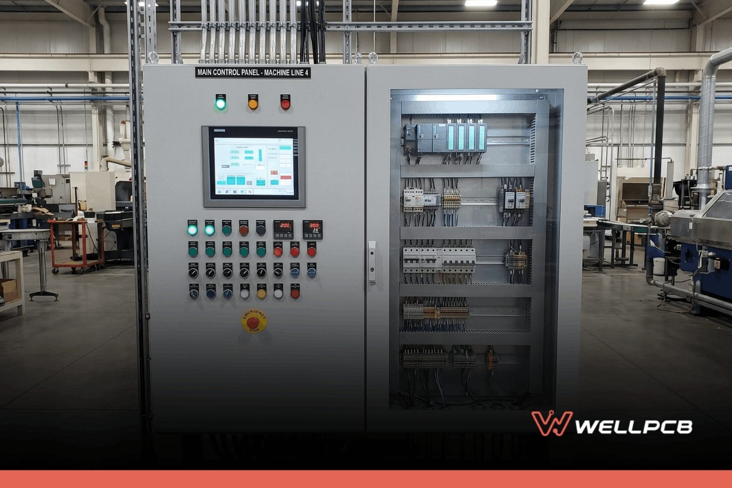
Industrial Control Components: What Each Part does in an Industrial Control Panel
On a 480 V packaging line, a single failed component inside an industrial control panel—a power supply, a breaker, an overload relay—can bring product...

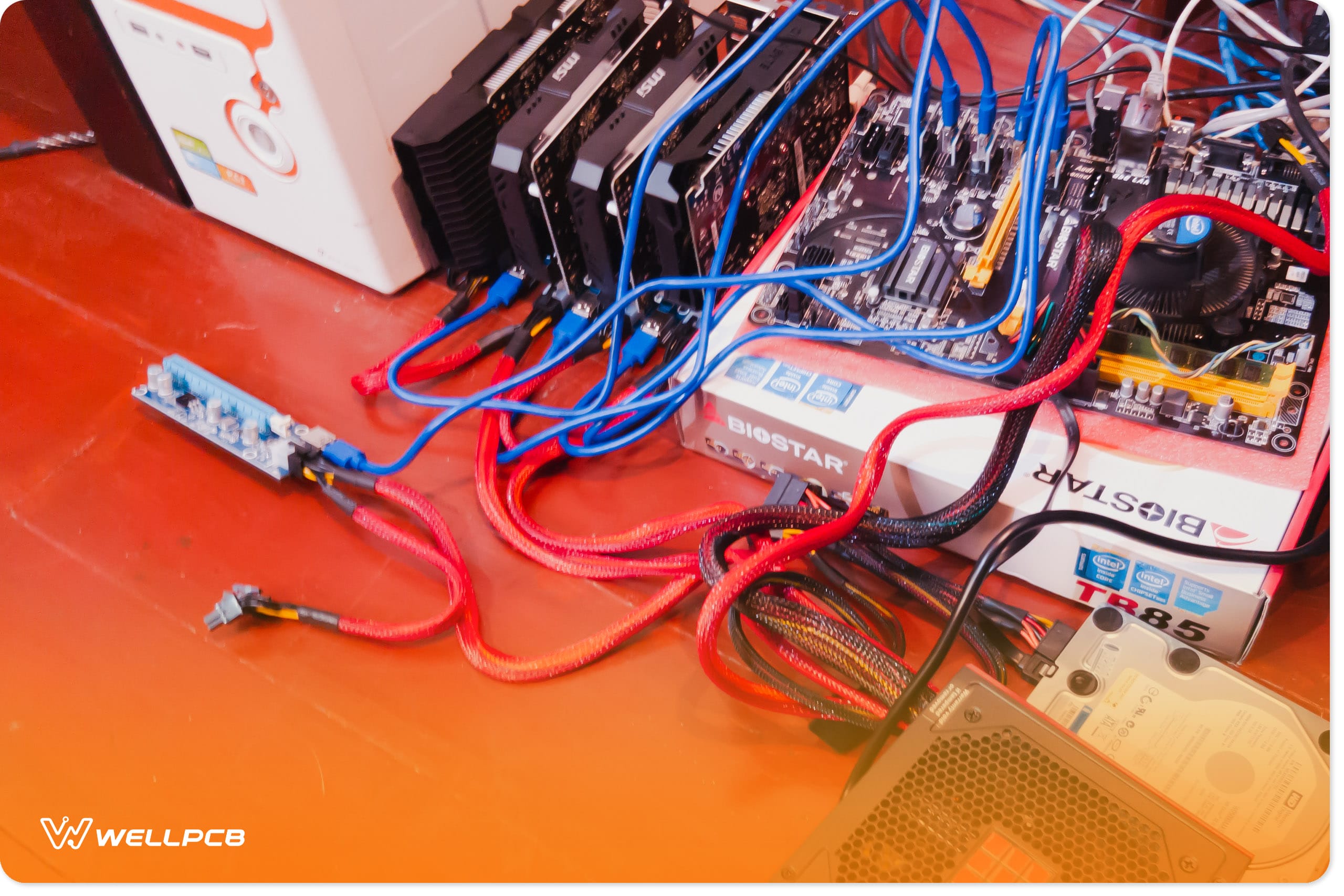
Truck Wiring Harness Manufacturers
Truck wiring harness failures rarely happen without warning signs in manufacturing and design. Some suppliers reduce costs by choosing lower-grade mat...

Top Automotive Wire Harness Manufacturers
Automotive wire harnesses ensure smooth operation by managing power and signal transmission across vehicle systems. They contribute to the overall rel...
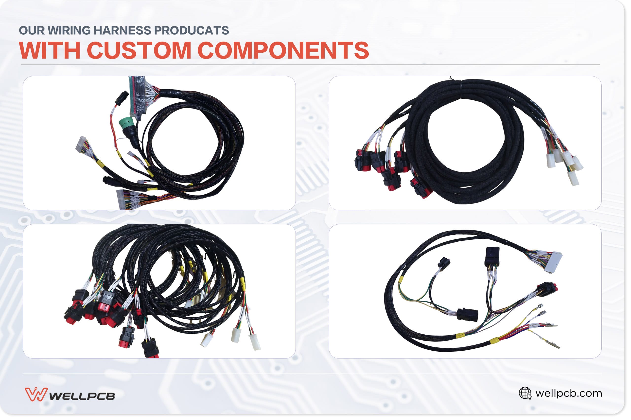
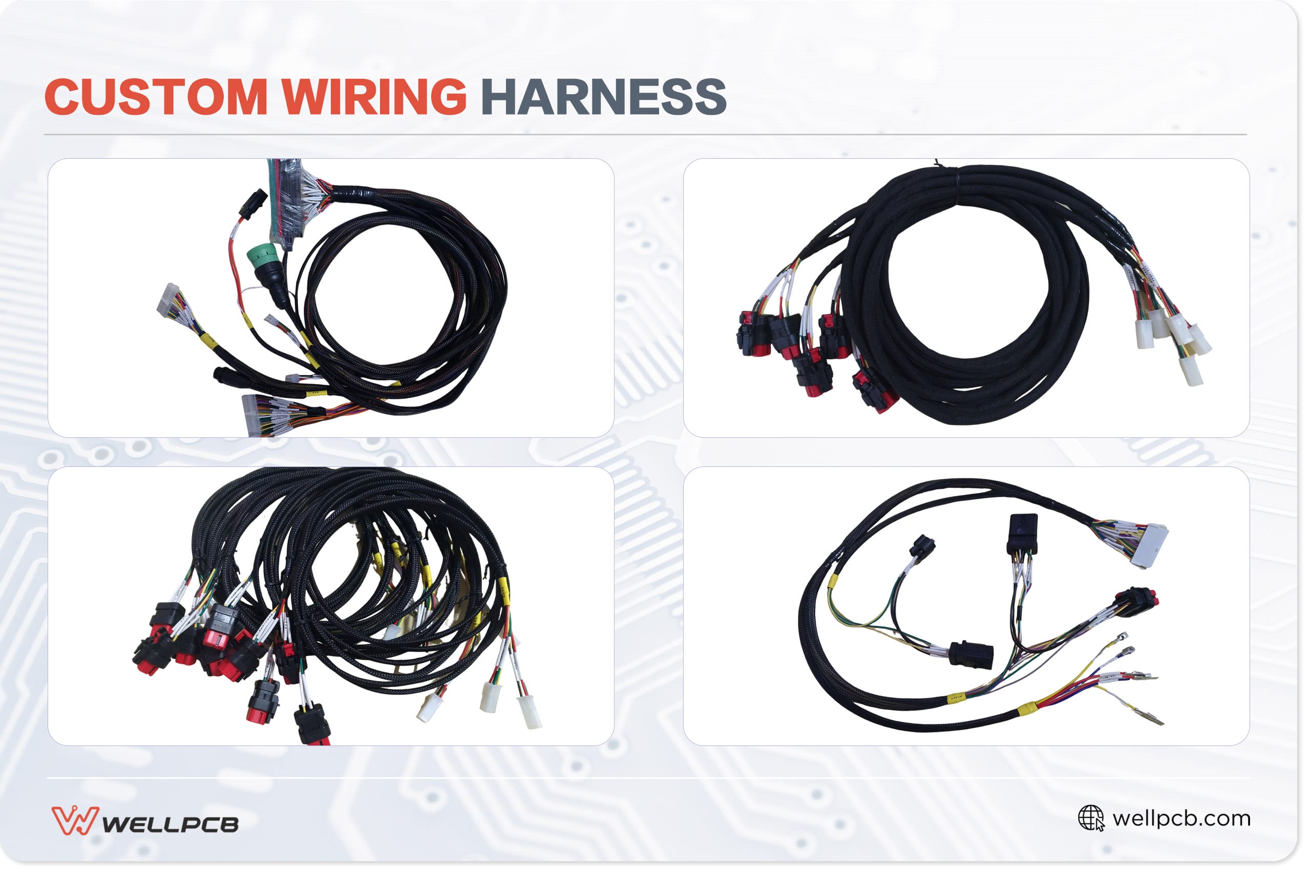
Custom Wire Harness Manufacturers
Custom wire harness manufacturers directly influence how electrical systems perform in real-world conditions. A properly built harness assembly organi...
OEM Wire Harness Manufacturers
Wire harness manufacturing influences electrical integrity and long-term equipment reliability for original equipment manufacturers. Inconsistent crim...

Robot Cable | Flexible Solutions for Robotic Cable and Automation
Industrial automation continues to accelerate, and the supporting infrastructure is scaling with it. Market analysts project significant market expans...

Cable Protection for Robotic Industry | Applications
Cable protection for robotic industry applications is critical because cables sit at the center of every robot’s performance. Power, data and control ...

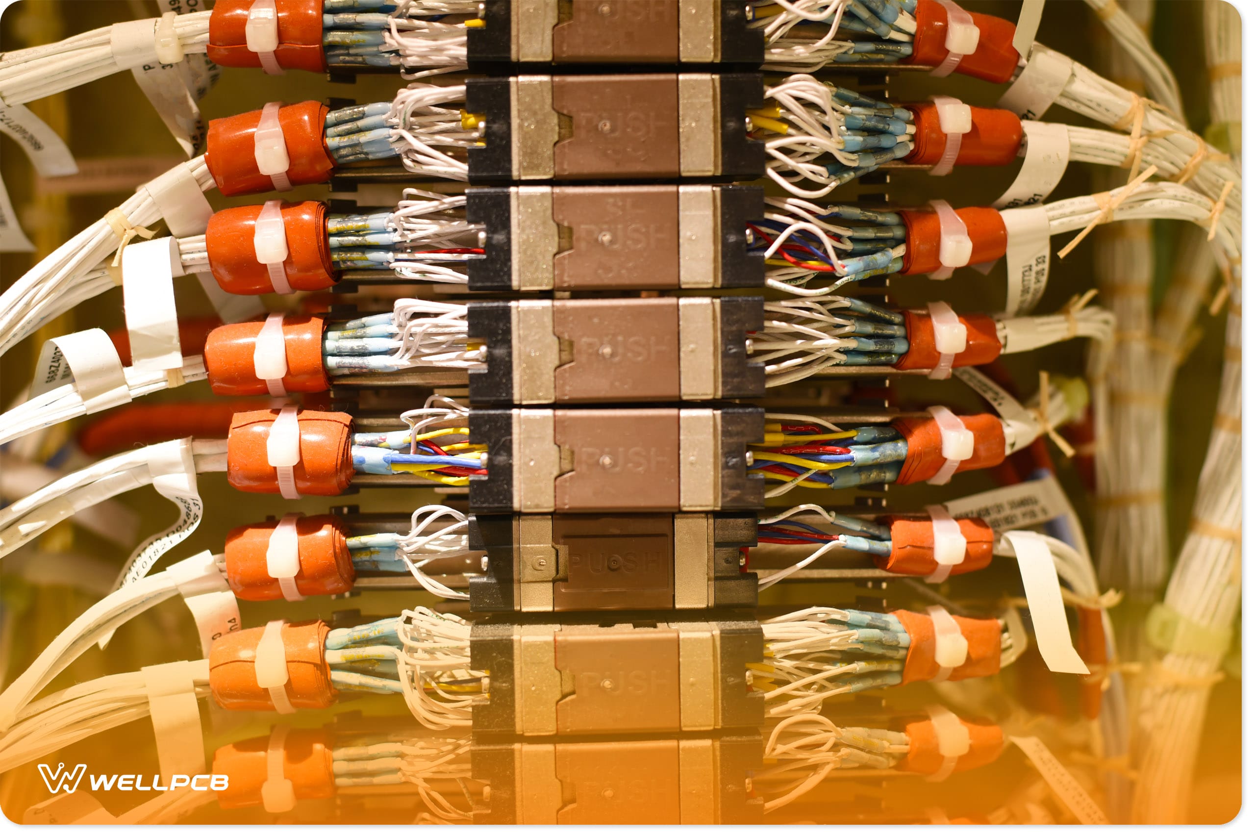
Top Industrial Wire Harness Manufacturers | Custom Wire Harnesses
Industrial systems depend on wiring that performs reliably under constant load, vibration and long service cycles. Choosing the right industrial wire ...

Top Aerospace Cable Assembly Manufacturers
Working with the right aerospace cable assembly manufacturers is essential for any aviation application. These cable assemblies must deliver consisten...

Top Waterproof Cable Assembly Manufacturers
Selecting the right waterproof cable assembly manufacturers is a must for products that operate where moisture, immersion and environmental stress are...

Top Appliance Wire Harness Manufacturers
Choosing the right appliance wire harness manufacturer directly affects product safety, service life and long-term production stability. In household ...

Top Medical Cable Assembly Manufacturers
Medical cable assemblies play a direct role in device safety, signal accuracy and long-term reliability across clinical environments. They carry power...
Robotics Cable Assembly Manufacturers | Robot Cable Solutions
Robotics cable assemblies form the electrical core of automation and robotics, powering control systems and enabling precise data transmission between...
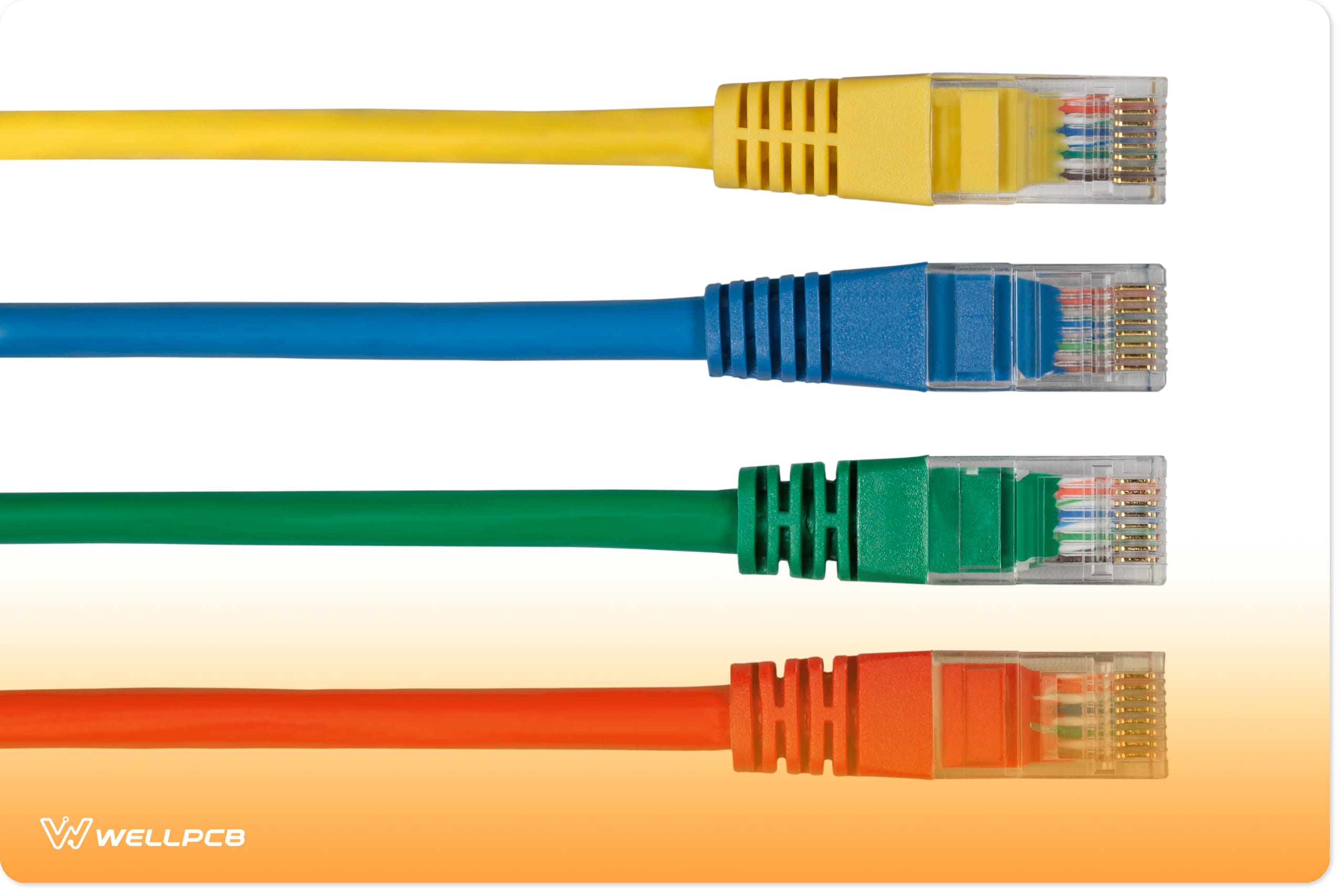
RJ45 Connector Pinout: Complete Guide & Wiring Diagrams
RJ45 connectors are synonymous with Ethernet connections because they are commonly used with CAT cables to facilitate data and power transmission acro...
Top 10 Cable Manufacturers in the World
Cables and wire harnesses are essential in industrial (machines and equipment), automotive, aerospace, power, communication, and electronic applicatio...
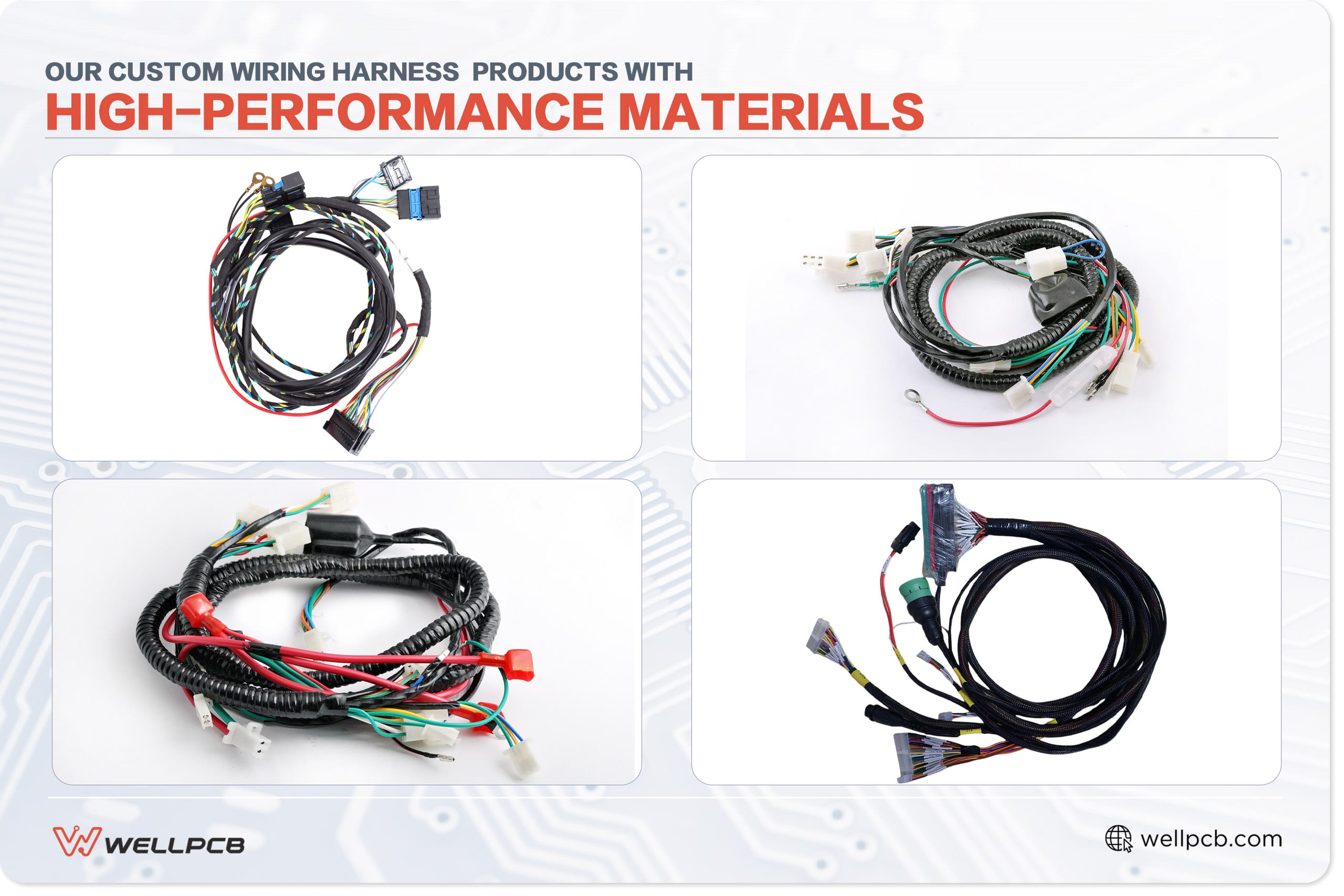
High-Performance Materials for Wiring Harnesses
Cars, planes, manufacturing equipment, medical devices, etc., have come to rely heavily on wire harnesses to handle the interconnections between inter...
Understanding Wiring Harness Components: Comprehensive Guide by WellPCB
Custom wiring harnesses are crucial for industries that require complex multi-cable systems. These systems power equipment and networks for the automo...

Comprehensive Guide to Designing Electrical Wire Harnesses
Similar to how blood vessels carry oxygen to and from the heart, electrical wire harnesses connect and feed power to complex electrical systems. Data ...
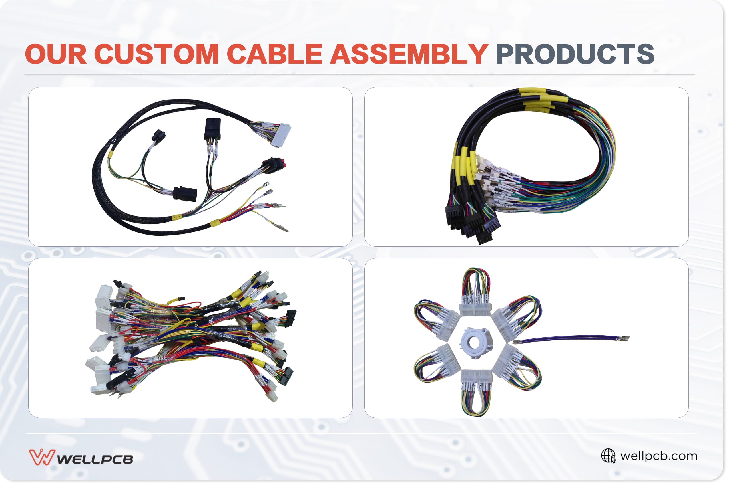
Benefits of Custom Cable Assemblies in Manufacturing
Cable assemblies play a critical yet often overlooked role in manufacturing. They are vital in streamlining and optimizing industrial operations. Most...
Best Practices for Wire Harness Assembly in Aerospace Applications
Modern aerospace vehicles no longer use mechanical controls. They rely on fly-by-wire systems, which use electrical wires to send control signals to v...
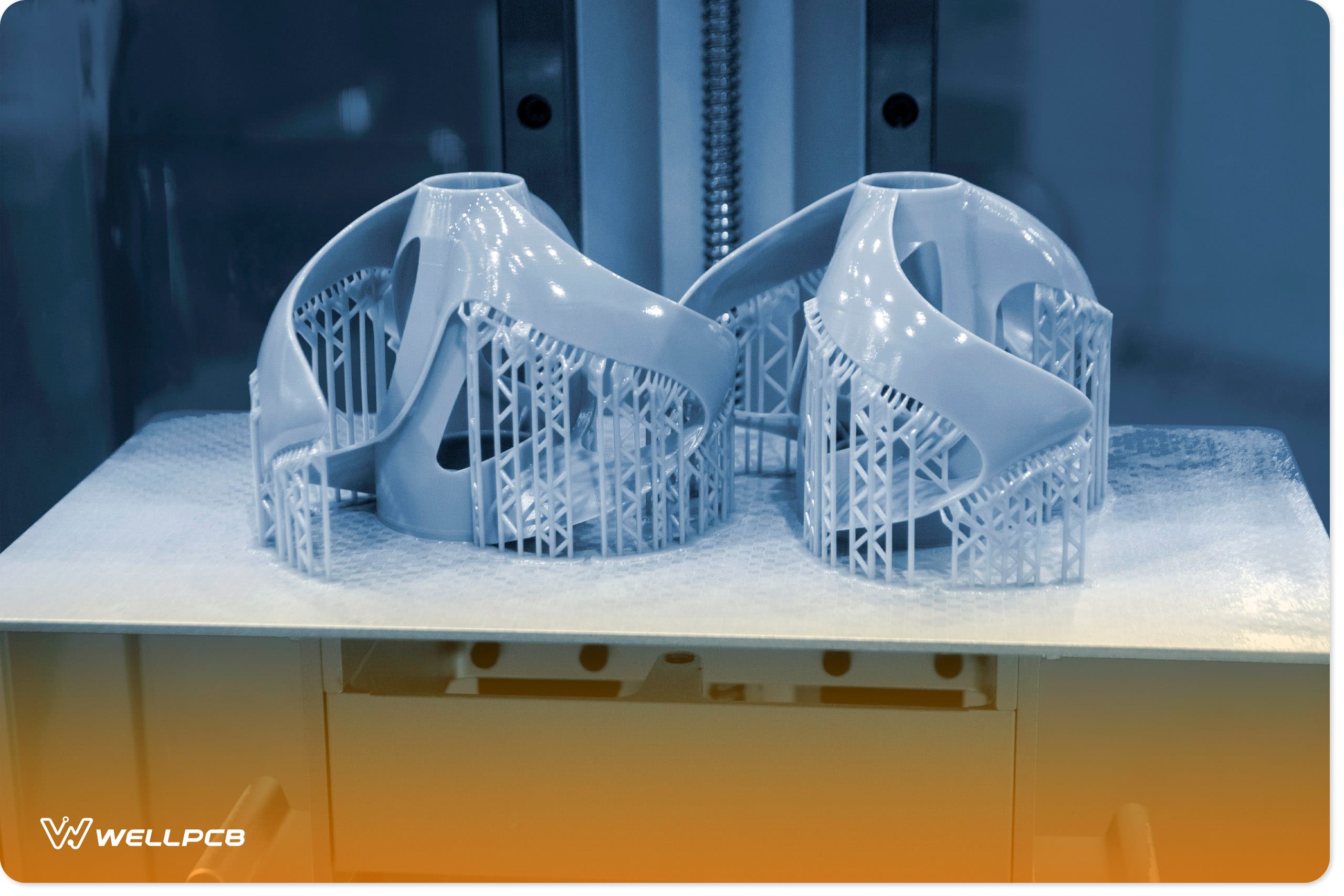
How to Reduce Costs and Increase Efficiency with 3D Printing
The manufacturing landscape is becoming increasingly competitive, especially in the 3D printing space. So if you plan to explore 3D printing in your b...

Case Studies: How Businesses Are Using 3D Printing to Innovate
With breakthroughs in materials, printers, and techniques, 3D printing has evolved from its original role as a tool for low-volume, rapid prototyping....
3D Printing for Custom Enclosures in Electronics: Enhancing Product Design and Functionality
The electronics industry is seeing a surge in demand for custom 3D-printed enclosures, as they offer business owners like you a cost-effective alterna...

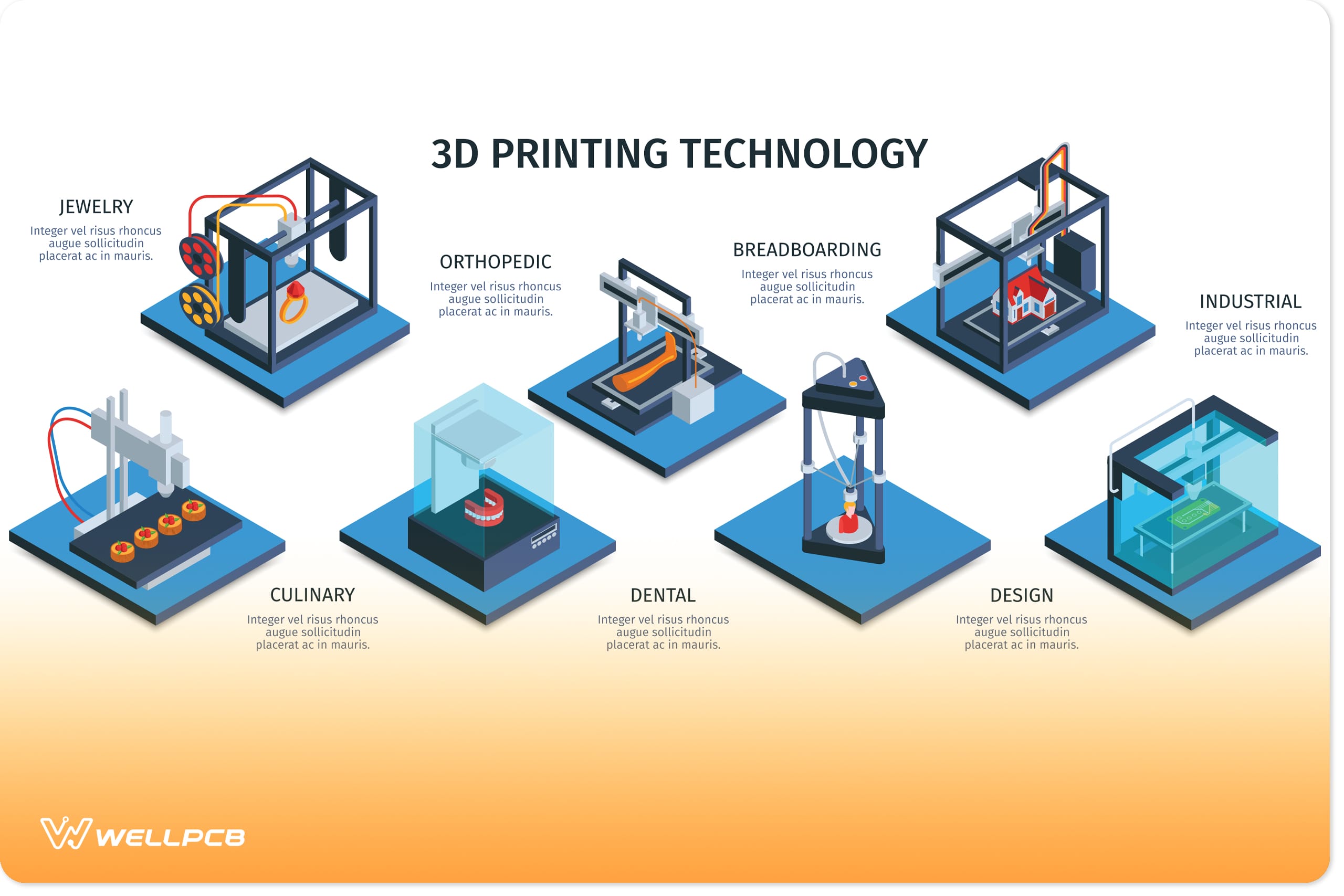
Top 10 Industries Transforming with 3D Printing Technology
3D printers aren’t usually associated with industrial manufacturing, largely due to their early adoption by hobbyists and small businesses. However, a...
12 Benefits of Turnkey PCB Assembly Services for Entrepreneurs
The importance of turnkey PCB assembly services cannot be overstated. Put simply, turnkey PCB assembly implies that the PCB supplier handles everythin...
The Ultimate Guide to 3D Printing Services for Large Enterprises and SMEs
3D printing services for businesses are essential for businesses today, as they enhance production efficiency, foster innovation, and reduce costs. Bo...
Circuit Simulators: A Guide to the Top 13 Tools
Circuit simulators allow you to evaluate the feasibility of your circuit designs, serving as virtual prototyping tools for printed circuit boards (PCB...
FDM vs. SLA vs. SLS: Which 3D Printing Technology is Best for Your Business?
When thinking of the best 3D printing technology for business (at least for plastics and resins), three terms come to mind: FDM, SLA, and SLS. Each te...

Integrating 3D Printed Components into PCB Design: Opportunities and Best Practices
Additive manufacturing, or 3D printing, is a relatively new technology with considerable potential to revolutionize the manufacturing of electric prin...

What is 3D Printing? An In-Depth Overview for Business Owners
3D printing, or additive manufacturing, is the process of creating 3D objects layer by layer. By simplifying the production process, it sets the stage...

3D Printed Circuit Boards (PCBs): A Game Changer for Electronics Companies
3D printed circuit boards (PCBs) are transforming the electronics industry by offering faster prototyping, reduced costs, and better design flexibilit...

3D Printing Software: Essential Tools for Business Success
When you think of 3D printing, the first image is often the printer itself. But the hardware alone is not enough; it needs the right software to manag...
The Complete Guide to 3D Printing Materials: What Your Business Needs to Know
Aside from the printer and 3D design software, the most crucial element in 3D printing is the material itself. The choice of material directly affects...

EMI Shielding in PCB Design: Unlocking Efficient Circuits
Electromagnetic interference (EMI) is an undesirable disturbance that disrupts electrical circuitry and impairs the functionality of printed circuit b...
6 Essential PCB Layout Guidelines for Great Designs
PCB layout guidelines are a set of design rules and best practices that ensure optimal PCB performance, reliability, and manufacturability. They cover...

8 Expert PCB Design Tips for Reliable and Manufacturable Boards
Even with advanced PCB design tools like OrCAD and Sprint-Layout, successful PCB manufacturing requires careful circuit design. This is because proper...
Thermal Management PCB Materials: How to Enhance Heat Dissipation in PCB Designs
Modern PCBs typically have complex structures and high densities, which inevitably leads to significant heat buildup. As such, effective heat manageme...

PCB Laminate Materials: Types, Properties and Considerations
It may seem slightly counterintuitive, but your printed circuit board’s (PCB) laminate greatly impacts how well it performs electrically. The laminate...
7 Top-Quality PCB Fabrication Services and Companies
PCB fabrication is the process of creating functional printed circuit boards from design files. This is typically done via a reliable PCB fabrication ...

Essential PCB Trace Design Methods for High Performance
PCB traces are essentially the blood vessels and nerves of the printed circuit board (PCB).
In the same way that human bodies can’t function without ...

Exploring the Latest Advances in PCB Manufacturing Technology
Printed circuit board (PCB) manufacturing technology has made significant strides in recent years. Yet, the manufactured products—the PCBs—often get m...

Comprehensive Guide to High-Speed PCB Design
Trends in printed circuit board (PCB) design have always been fueled by advancements in computing technology. The recent increase in demand for high-s...

Comprehensive Guide to Industrial PCB Manufacturing
Industrial PCBs are designed to perform reliably in demanding environments. This resilience is essential for applications in the transportation, defen...
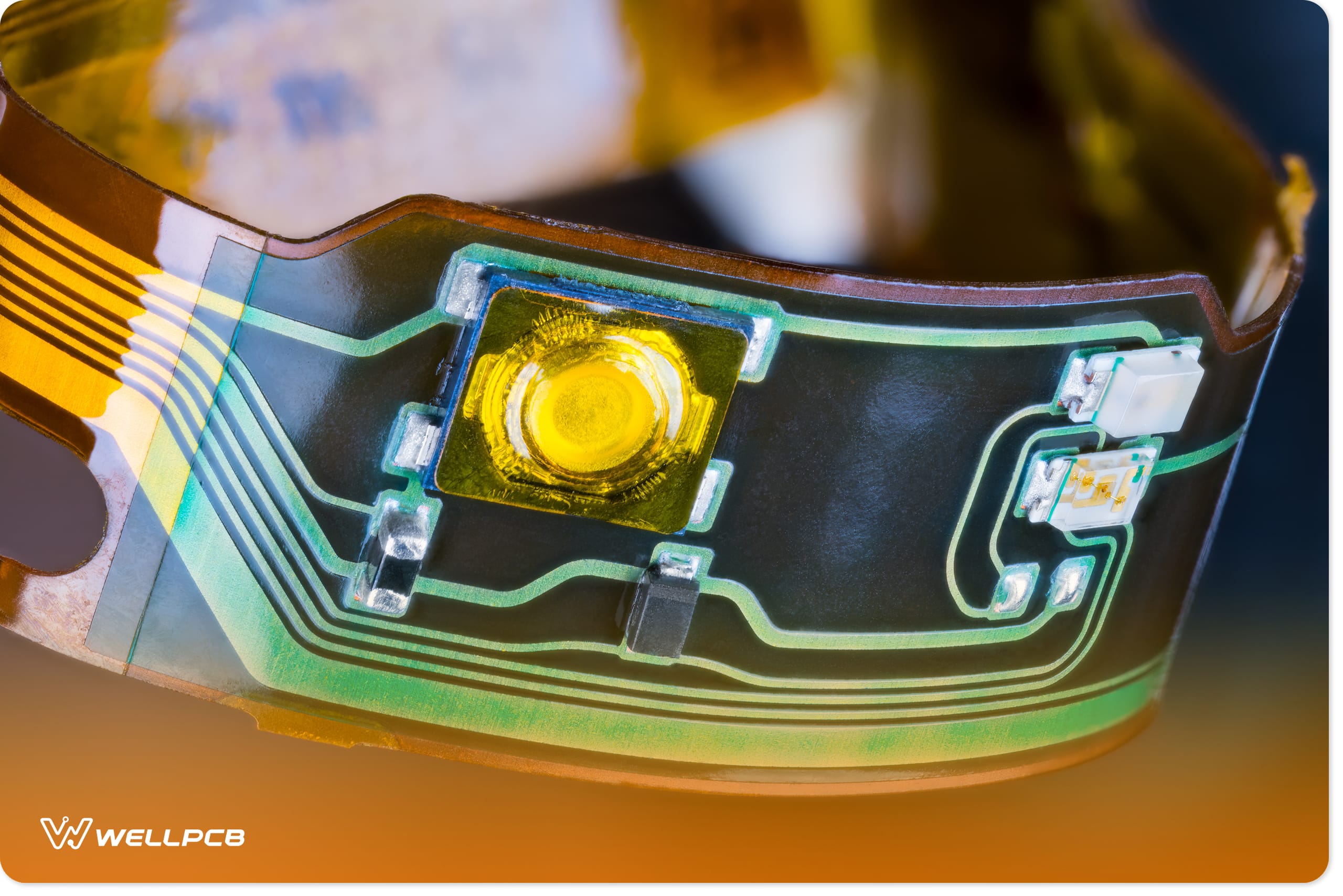
Comprehensive Guide to Flexible PCB Manufacturing
Flexible printed circuit boards (PCBs) are small, bendable, and reliable circuit boards. They’re mostly used in small modern electronic devices where ...

A Complete Guide to PCB Assembly Standards
PCB assembly involves multiple intricate processes that demand meticulous attention to detail. Various professional bodies set standards guiding these...
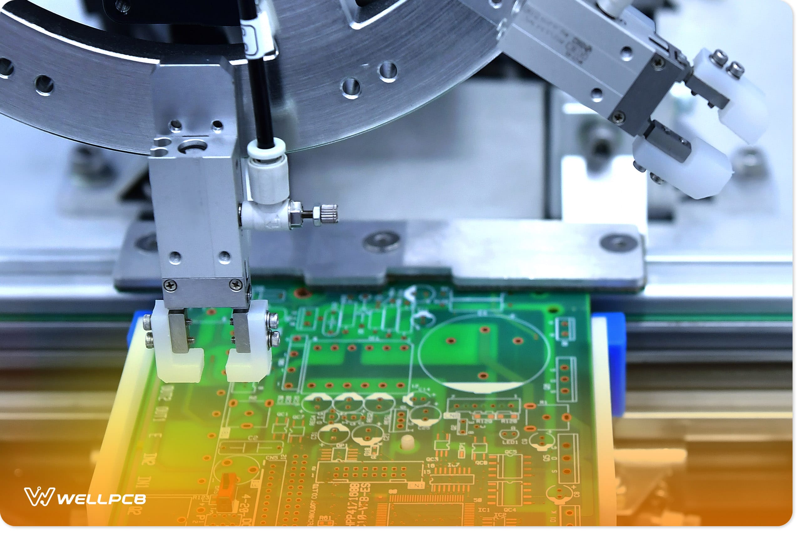
The Ultimate Guide to Automated PCB Assembly
As electronic devices get smaller, ensuring PCB assemble precision becomes increasingly challenging. Thankfully, automated PCB assembly addresses this...
The Comprehensive Guide to PCB Manufacturing Process
Printed circuit boards (PCBs) are the bedrock of modern electronics. And yet, because they seem like such simple devices, people often underestimate t...
Ensuring Top: Notch Quality in PCB Assembly: A Comprehensive Guide
Every home, business, and industry relies on electrical and electronic equipment, and printed circuit boards (PCBs) are their building blocks.
PCB as...
PCB 101: Your Beginner’s Guide to Printed Circuit Boards
Printed circuit boards (PCBs) are the backbones of modern electronics. Without them, we wouldn’t have computers, communication devices, and countless ...
How to Correctly Understand The Ball Grid Array Soldering Technology
The pitch size is reducing significantly as the electronic devices are getting smaller and smaller in size. The demand is to place the electronic comp...

Step-by-Step Guide to Perfect PCB Silkscreens
How to Get a Satisfied PCB Silkscreen: Look at a printed circuit board (PCB) with all components and wiring placed on it (Figure 1).
It looks like a...

Achieve Top Quality with Attractive Purple PCBs
When selecting a printed circuit board, you must choose the right colors for the solder mask.
The boards come in various colors, including traditiona...

An Ultimate Guide To Prototype & PCB Assembly Testing
On PCB Testing, PCB applications have become increasingly popular and diverse.
At the moment, PCBs manufactured by engineers power circuits that run...
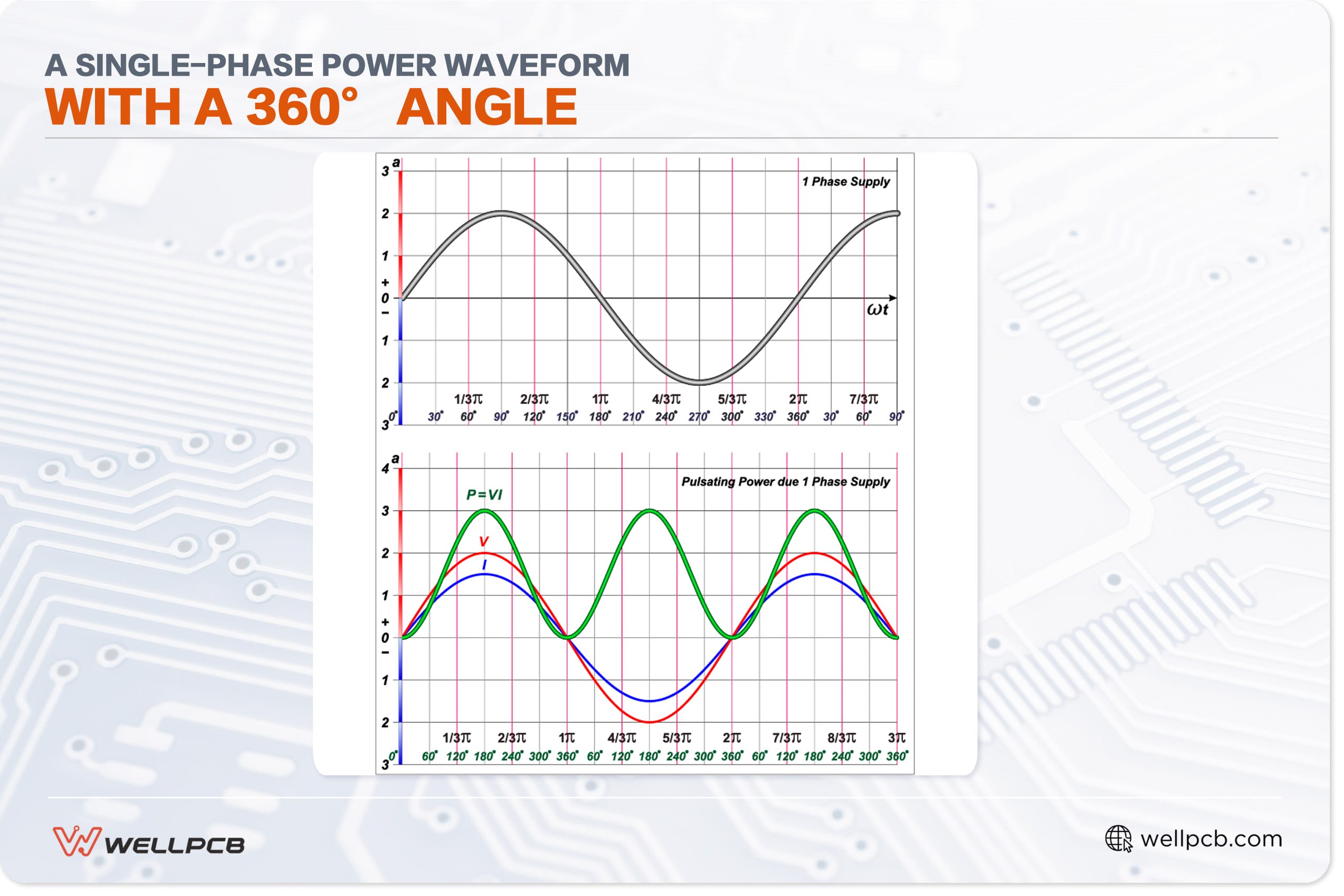
Difference Between Single Phase and Three Phase
In the 21st Century, there’s no denying that electricity has made life a lot easier. From the application of single-phase power supply in residents an...

HDI PCB Manufacturing: Microvias, Stackups & Design Rules
When designing PCBs, you might be worried about the additional costs and the increasing number of layers. However, with HDI PCB technology, manufactur...

Understanding the Differences between PWB and PCB
The article compares Printed Wiring Boards (PWB) and Printed Circuit Boards (PCB).
PWB refers to boards with basic wiring without complex circuitry,...

What You Need to Know About 4-Layer PCBs
If you're looking for a more advanced PCB, you might want to consider a 4-layer PCB.
This type of PCB has four layers, which allows for more complex...
Key Steps to Making DIY Circuit Boards
A printed circuit board (PCB) is the basis of all electronic components.
A PCB ensures an excellent electrical connection by featuring pre-designe...
The importance of IPC-6012 and IPC-A-600 in PCB production
The IPC (Institute of Printed Circuits) is a global trade association that serves PCB and electronics assembly industries. IPC verifies the quality of...
A Comprehensive Walkthrough on PCB Assembly Processes and Components
As the backbone of modern electronics, printed circuit boards (PCBs) need to function reliably over extended periods of time. Their durability and lon...

Top PCB Design Tools Guide(2025)
For the circuit board designer, the wide variety of PCB design software available in the market can pose an overwhelming range of options.
Understa...

Mastering Your DIY Projects: A Comprehensive Guide to Arduino Nano Pinout
Arduino’s wide range of single-board microcontrollers and kits are perfect for amateur robotics hobbyists and seasoned engineers. They’re affordable, ...
Easy to Understand Guide to Circuit Board Parts
A printed circuit board (PCB) is a collection of copper traces running through a substrate. Consequently, it serves as the foundation for most electro...
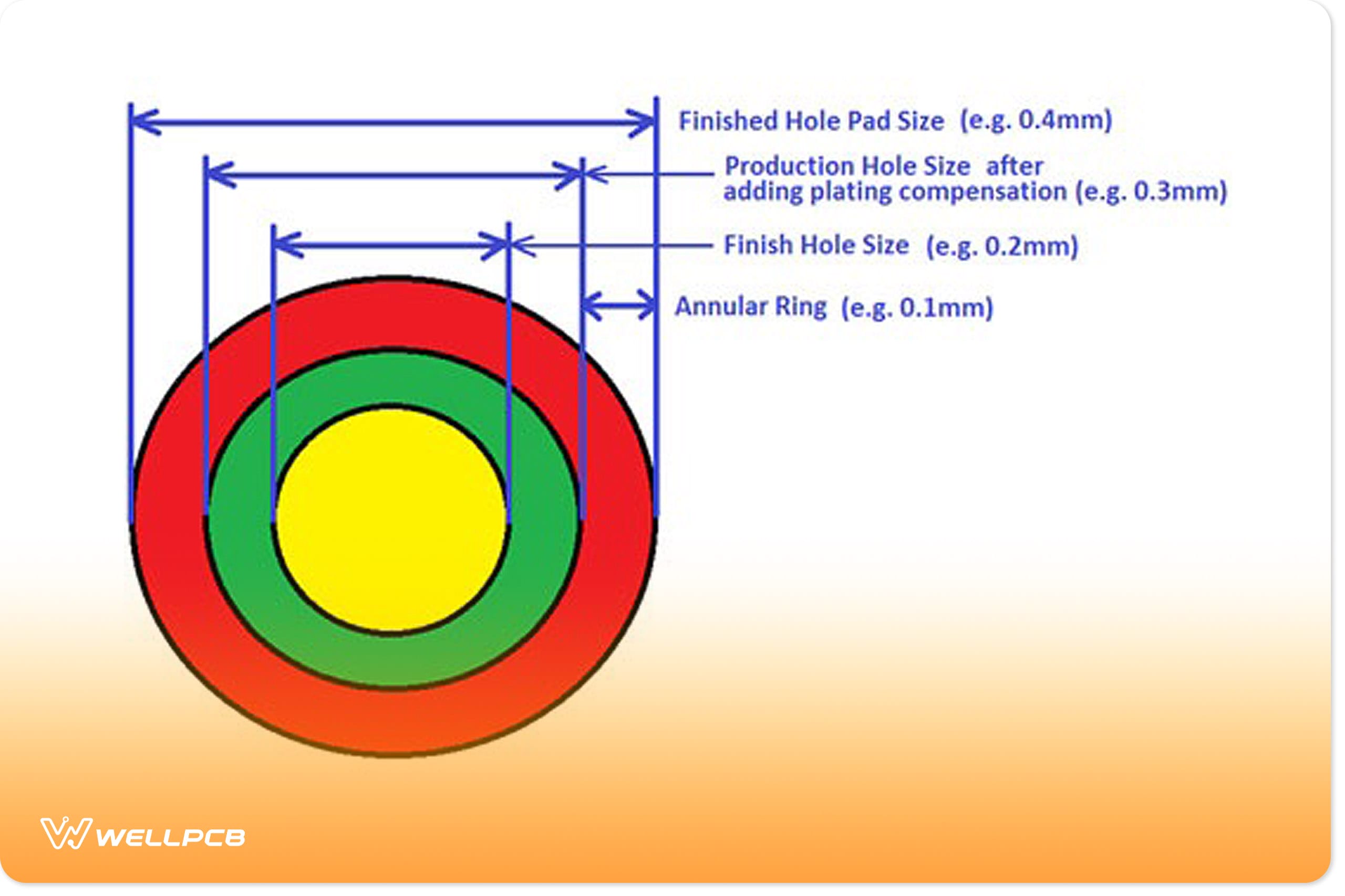
Everything You Need to Know About PCB Annular Rings
PCB Annular ring is one of the biggest concerns that a lot of PCB designers face. While you could be 100% sure that you've placed your via in the midd...
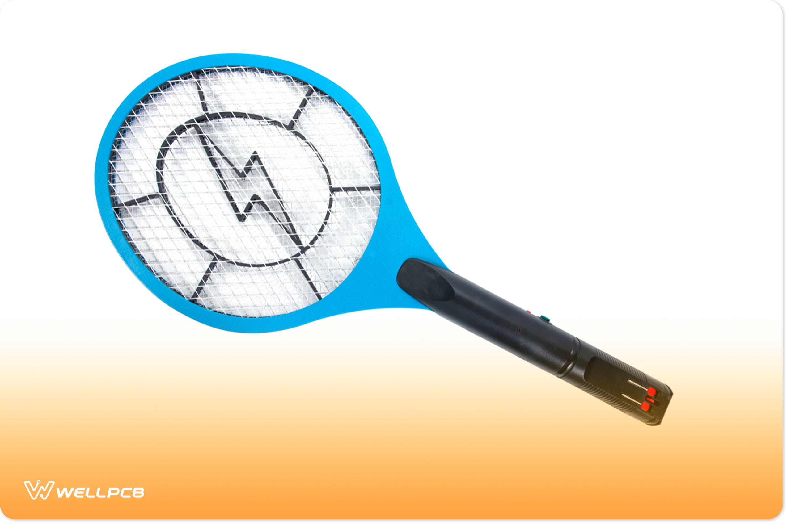
DIY Bug Zapper Circuit Projects for Eliminating Insects
We are all aware of the irritation mosquitoes bring to our day-to-day lives.
Thus, it is only natural if you want to get rid of them for good.
Bes...

EasyEDA Tutorial: How to Design a PCB Schematic Step by Step
Are you new to PCB design?
EasyEDA can benefit beginners or those who need reliable software to test their ideas.
It is a free PCB design softw...
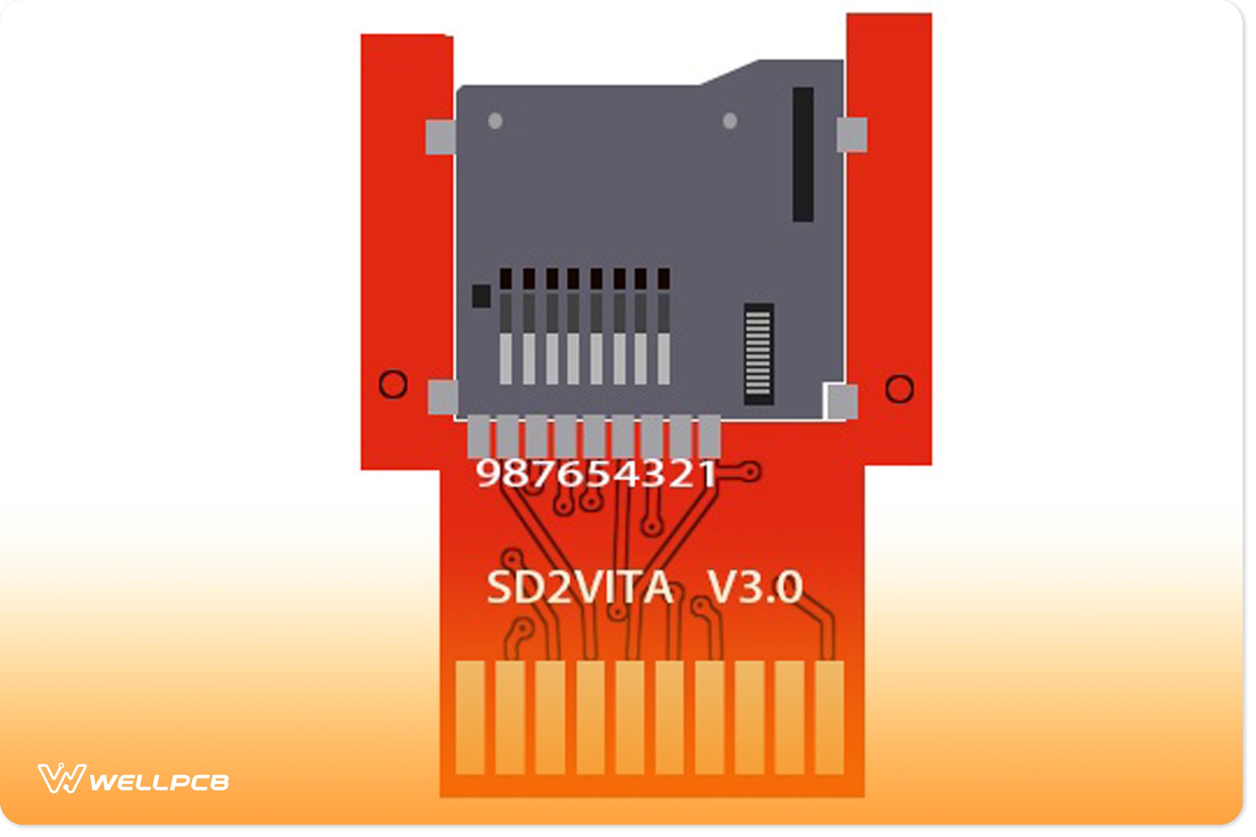
The Ultimate Guide to Using SD2Vita
SD2Vita is an exciting niche for anyone interested in the mechanical assembly of PCBs because it touches on what most of us love: PS gaming. SD2Vita i...

Understanding the Differences Between PCB and PCBA
Technological advancements over the past decade have been nothing short of awe-inspiring. These feats of human genius and innovation would mean nothin...

Understanding Solderability Testing for PCBs
It would be best if you had solder testing to minimize component solderability issues in PCB manufacturing. You can use preventive measures, such as t...

Comparing Chip Antenna and PCB Antenna in a Detailed Guide
Understanding the Chip antenna Vs PCB antenna comparison is important in choosing antennas for your embedded designs. Your electronic device needs an ...
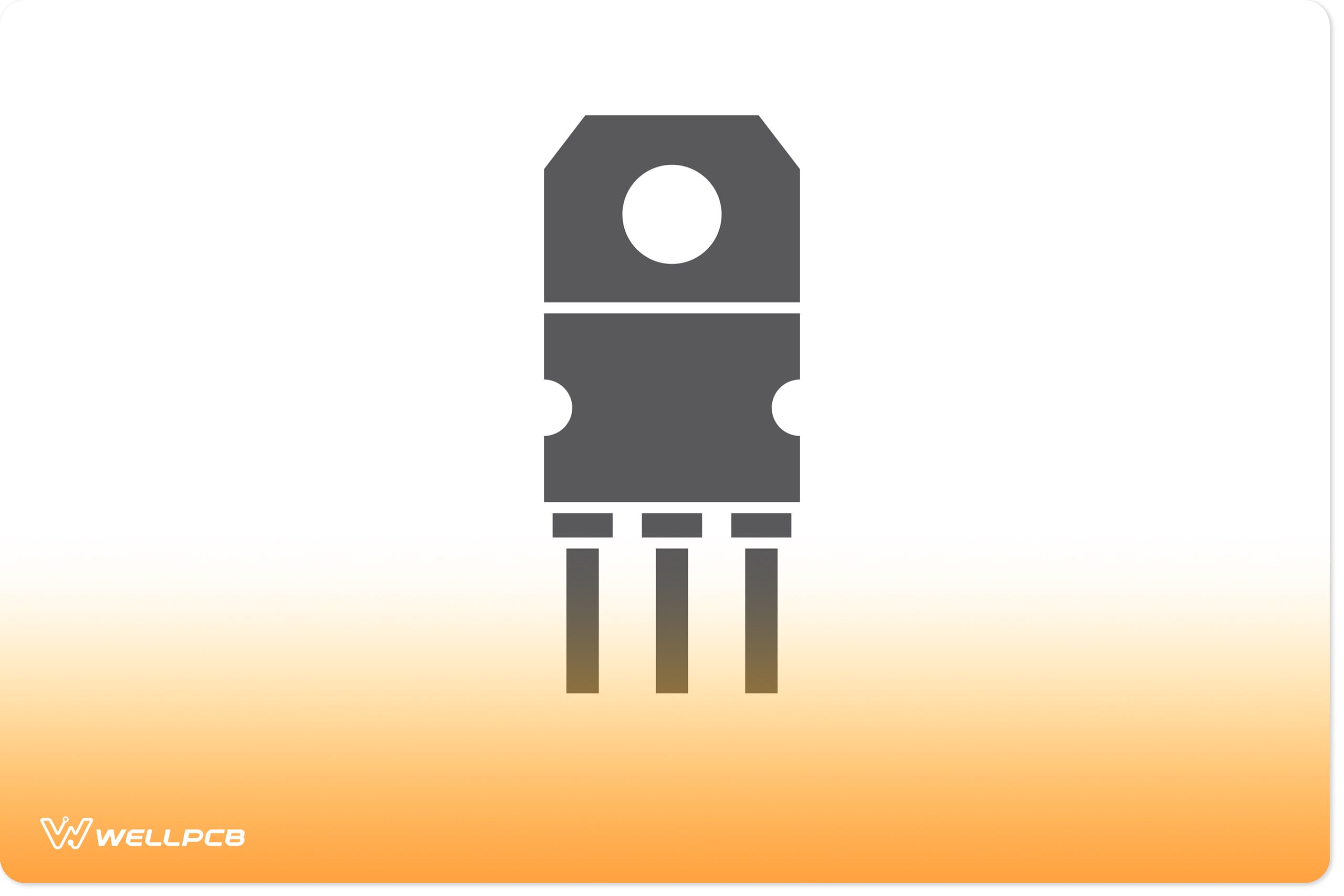
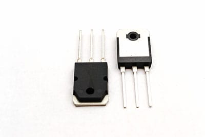
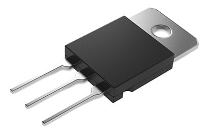
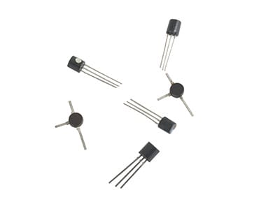
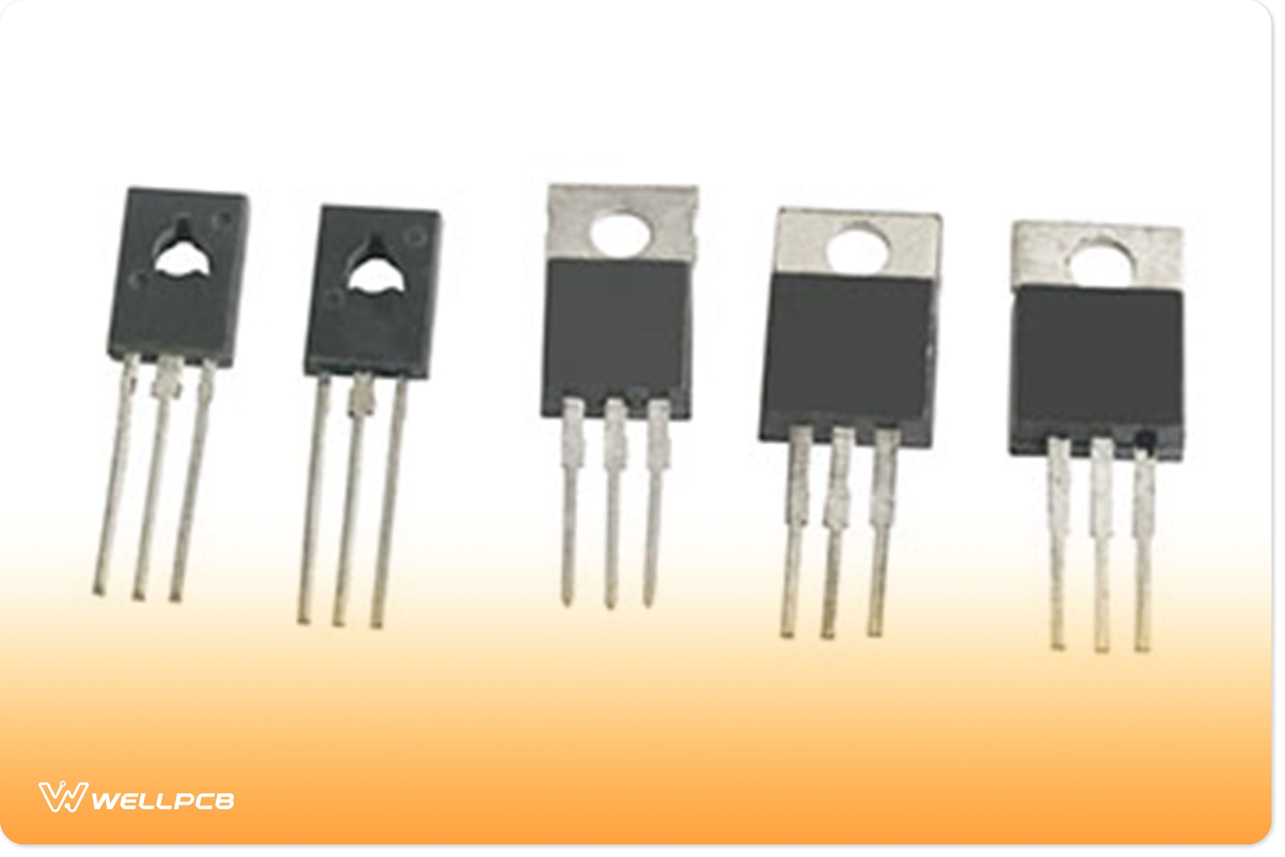
How to Use the 2N3055 Transistor Features and More
The 2N3055 transistor is part of a group of electronic transistor devices. The original 2N3055 works best as a low-powered, simple switching device.
...

What’s the Difference Between Digital Input and Analog Input
The following guides compare digital input vs. analog input.
You must understand the differences between these two technologies.
This is especially...
Everything You Need to Know About Variable Power Supplies
Have you been asking what a variable power supply is?
Here we have the answer for you. Therefore, we will help you know what a variable power supp...

How To Use Turnkey PCB Service For Efficient Production
PCB manufacturers worldwide are in a race to ensure their manufacturing costs, but not at the expense of quality. PCB makers want to ensure product qu...

How to Make a Radio Frequency Jammer with This DIY Guide
Radio signals are essential for communication.
Nonetheless, there are scenarios whereby you may not want frequencies from a radio transmitter to r...
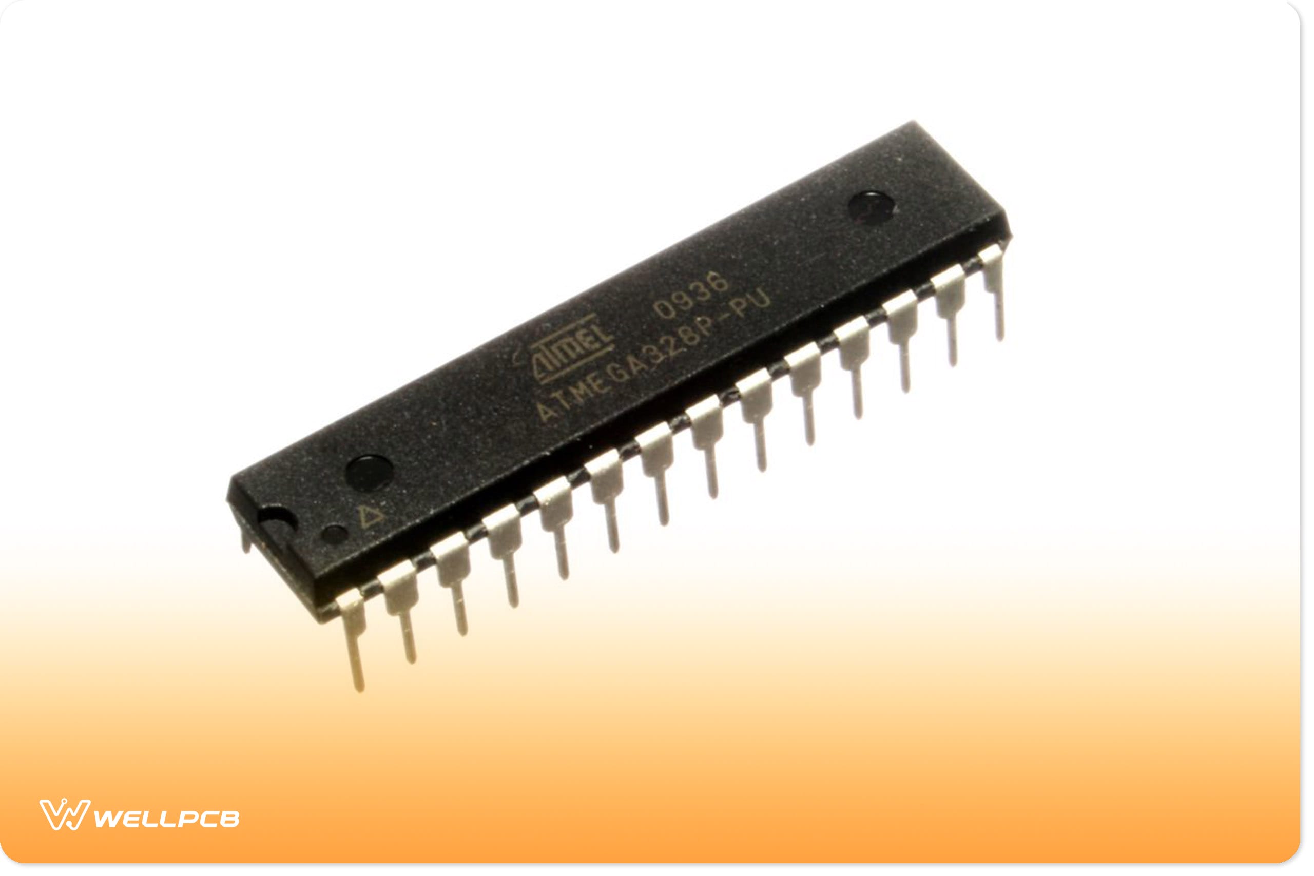
A Detailed Explanation of the ATMega328P
The microchip or integrated circuit invention is one of the greatest discoveries.
Thus, the majority of modern products today use microchip techno...

Exploring the Properties and Uses of FR4 Material
FR4 material is a glass-reinforced epoxy laminate commonly used in applications requiring high stiffness and rigidity, such as printed circuit boards ...

How to Produce RoHS 2 Compliant PCB Products
In the manufacture of electrical and electronic equipment (EEE), where PCBs belong, certain restrictions apply. Mostly, these restrictions here guide ...

How to Make Electronics That Meet REACH Regulations
Through the years, the global PCB manufacturing industry has undergone numerous changes. Some of these changes have to do with rules and regulations. ...

What a Pulsing LED Circuit Is and How to Build One
Does your project involve creating light effects, and you're looking for the best method to make them? If your answer is yes, you should consider the ...

Small Outline Integrated Circuit-How To Choose
On Small Outline Integrated Circuit: With the popularity of integrated circuits, the need for them in a circuit board grew.
In the early days, integ...
PCB Cross-Section Analysis: Technology, Process, and Benefits
Even the most reliable PCB fabrication processes cannot guarantee the ultimate quality of a finished product without thorough testing. For instance, s...

How to Master More Skills for Rapid Design
A rigid-flex PCB design is, by far, considered a complex PCB to design since it requires a mastery of technical skills to make one. Indeed, it stands ...
Useful Tips and Procedure Guidance for CCA Electronics
In CCA electronics, a circuit card is easily inserted in the slots for expansion in the computer, increasing the given computer's capabilities.
The ...

Get an In-Depth Understanding of the MFD Meaning in MFD Capacitors
MFD capacitor is among the vital electrical components of a printed circuit board (PCB) network. They work by storing energy in their electrical field...

Everything That You Need To Know About PCBs With Blind Vias
Are you looking for more space in your extremely packed PCB design? Are you tired of drilling so many holes through your PCB? Did you know that there ...

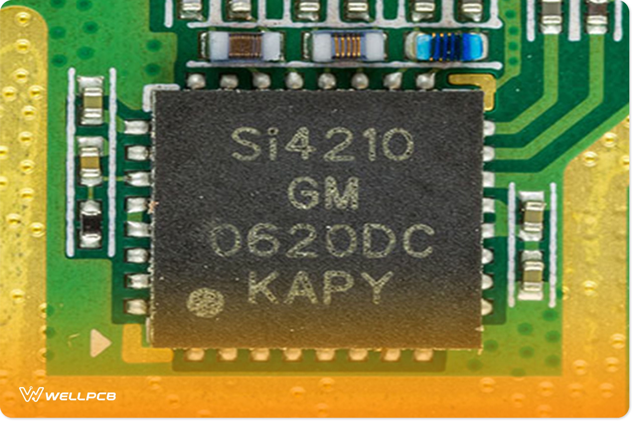
The Ultimate Guide to Understanding 94V-0 Circuit Boards
In a nutshell, the 94V-0 Circuit boards are defined as circuits inscribed on PCBs (Printed Circuit Boards) that have met the UL 94V-0 flammability tes...
LGA vs BGA Socket: Key Differences & Comparison Guide
Gone are the days of bulky integrated circuits (ICs). Today, sleek, compact ICs power the world’s most advanced CPUs, enabling smaller, faster, and mo...
Why Are Motherboards Green? The Colors and Science Behind PCB Design
When you think of a motherboard, what color comes to mind? For most people, it’s green. This familiar color has become closely linked with these essen...
Soldering Techniques and Tools: A Comprehensive Guide
If you’re an electronics enthusiast looking to master soldering for your projects, you’ve come to the right place. This guide covers all the essential...

A Beginner’s Guide to Fiber Circuit Communication Systems
In the past, electrical cabling was the main thing till people needed high bandwidth over a long distance.
Unfortunately, the electrical cables coul...
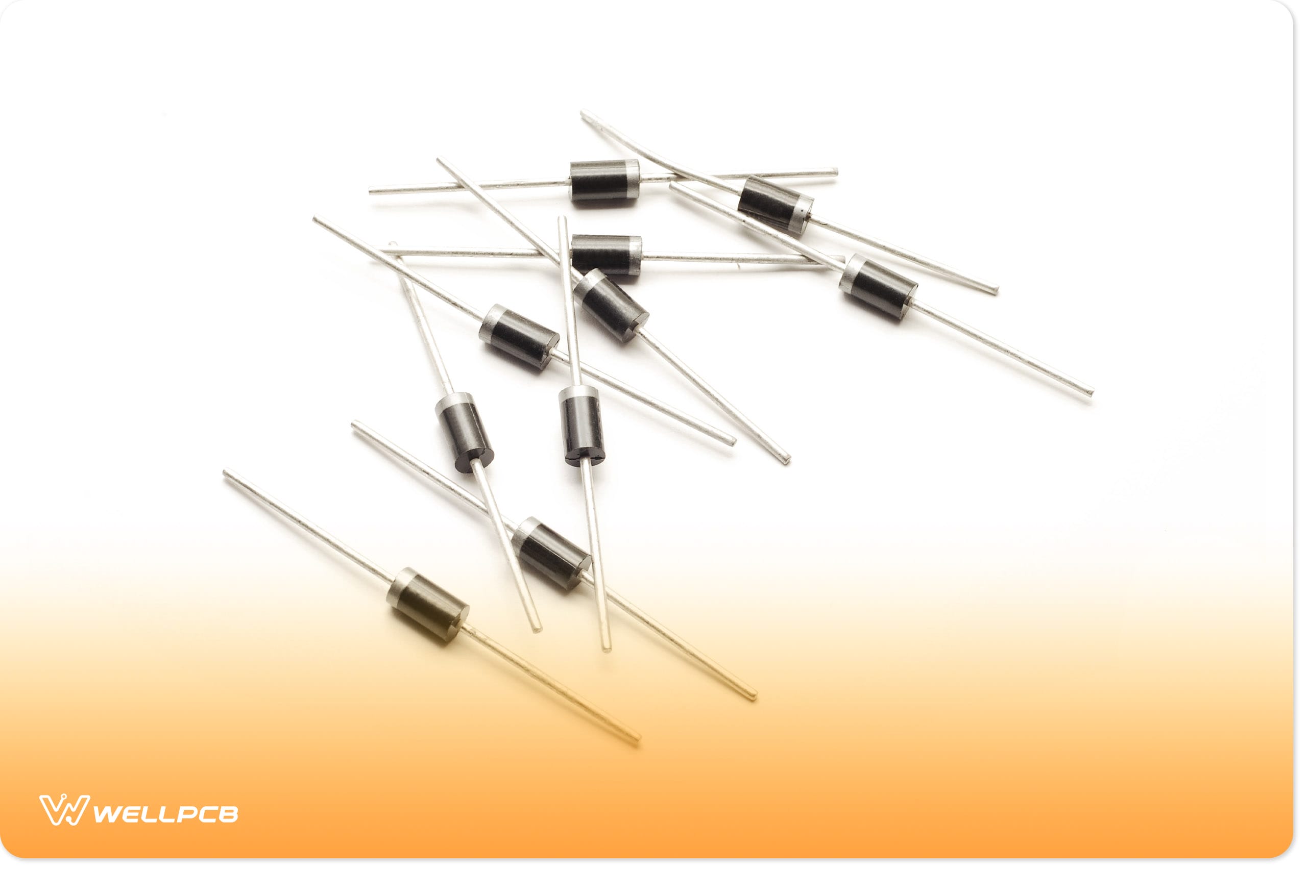
Best Ways to Test a Diode: With & Without Multimeter
If you’re an engineer or electronics designer, you know that almost every circuit features diodes.
Indeed, they are one of the most common component...

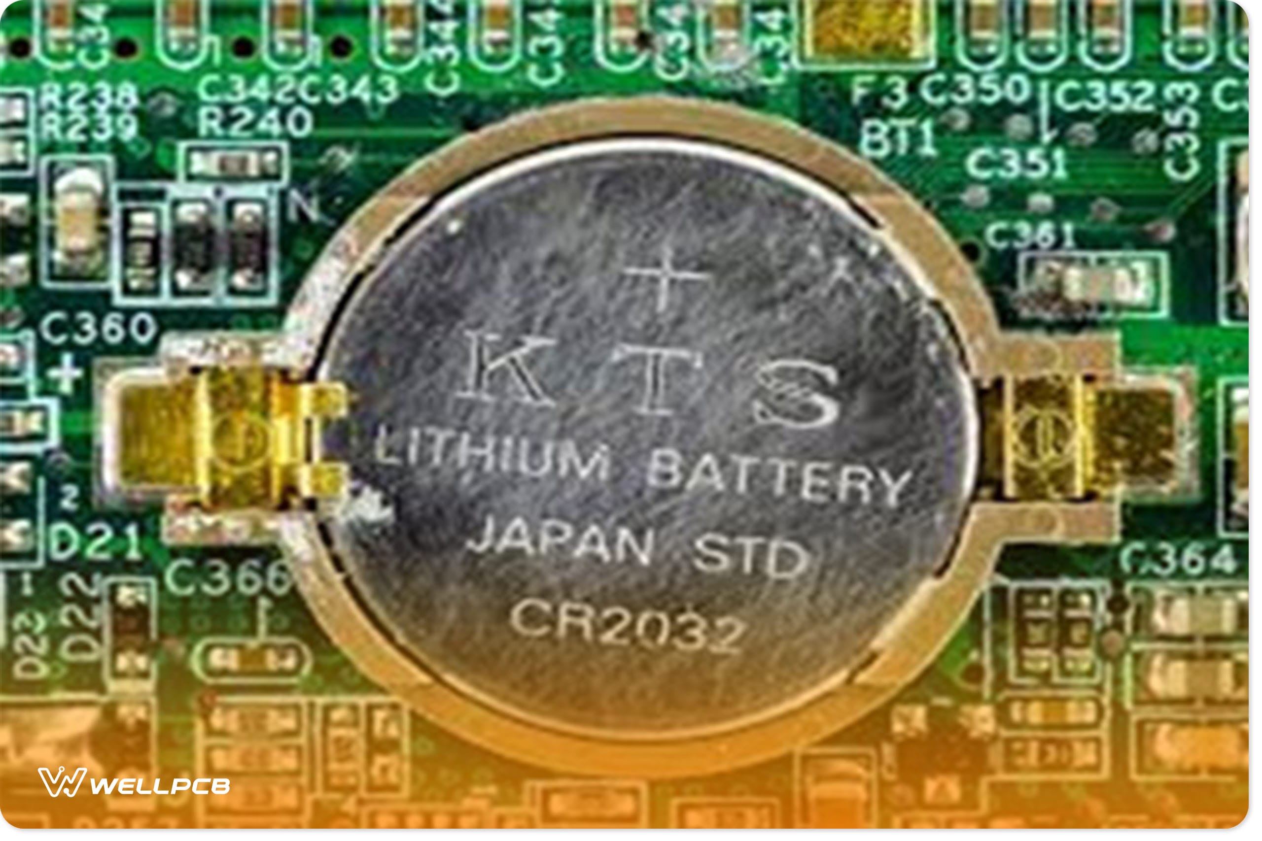
Demystifying Coin Cell Batteries: CR2025 vs CR2032
Have you ever replaced the small battery in a device, only to find it still doesn't work? Coin cell batteries like CR2025 and CR2032 continue to power...

The Ultimate Guide to PCB Production Process
Every printed circuit board has a unique function. Therefore, PCB production is always different and includes many complex steps.
First and foremo...

What a Barebone PCB Is and How to Use It Updated
Barebone PCB is a cost-effective and miniaturized alternative to Arduino PCBs.
You can make these boards within one hour since they are ideal for DI...

Diode Clipping Circuit: A Close Look At Different Types of Clipping Circuits
Do you deal with electronic projects that involve you protecting it from a high voltage spike?
Then, it would help if you used a diode clipping circu...

Guide to Better Sound Quality with Subwoofer Amplifier Circuits
Are you looking for a way to achieve a noiseless and high-quality bass sound? What you need is a subwoofer amplifier circuit. Not only is it compact b...

PCB Welding-Methods and Techniques on How to Reduce the Problems
PCB welding, commonly referred to as PCB soldering, enables components to form reliable electrical connections on printed circuit boards (PCBs). No ma...
14 Tips on Designing a PCB Programming and Testing Board
The article from WellPCB provides comprehensive insights into PCB programming and testing, focusing on modern PCBs' integrated circuitry which enables...
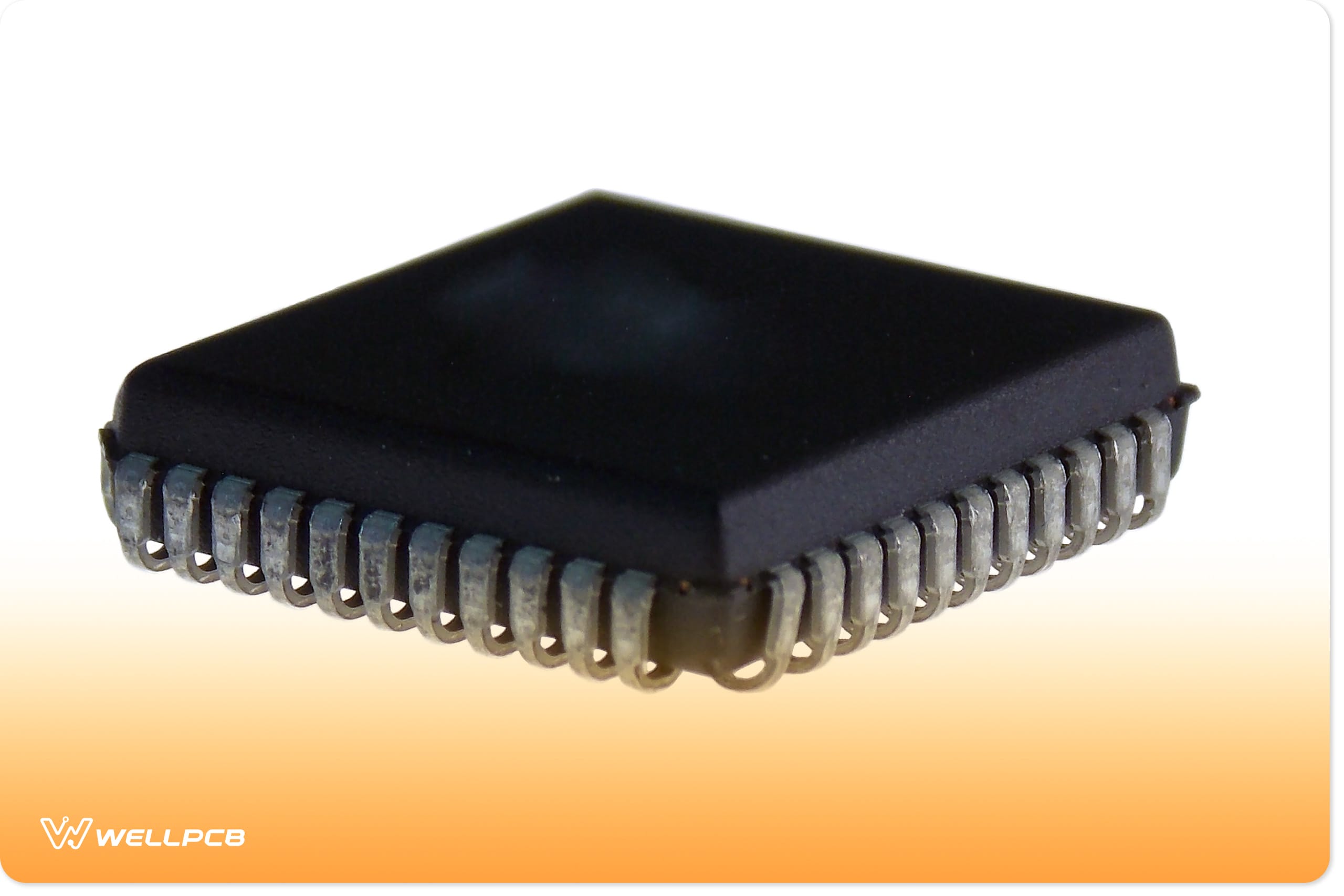
Understanding PLCC Packages and How to Use Them
From bump chip carriers (BCCs) to quad flat packs (QFPs), there are many types of surface mounted packages (SMDs). The plastic leaded chip carrier (PL...
A Complete Guide to STM32 Pinout and Microcontroller
Microcontrollers are shaping the world of electronics in different ways. You find them in various fields like robotics, automotive applications, etc. ...
Everything You Need to Know About PCB Thermal Pads
Are you familiar with heat transfers within the CPU? Then, you may have come across a PCB thermal pad. But do you know how or where it works?
Typical...
An In-Depth Guide About Black PCBs
You might have seen a black PCB. The actual color of the PCBs is the solder mask, not PCB itself.
In most cases, the Printed Circuit Boards are green...

Guide to Avoiding Mistakes with LED Polarity in PCB Manufacturing
The next time you’re sitting in traffic, look at your vehicle's dashboard display. Outside, you might also notice traffic lights with indicator screen...
Your Roadmap to Success with PCB Manufacturability Guidelines
When designers plan the layout of their PCBs, they sometimes fail to consider how it impacts manufacturability. The aim of PCB design should be to cra...

Understanding the PCB Assembly Showdown Between SMT and THT
Printed circuit board (PCB) assembly in electronics manufacturing is vital when creating functional devices. Correct PCB assembly techniques rely on c...
The Ultimate Guide to Conformal Coating in PCB Manufacturing
Printed circuit boards (PCBs) are vital in the electronics industry, enabling devices to operate.
However, for PCBs to function, their various com...
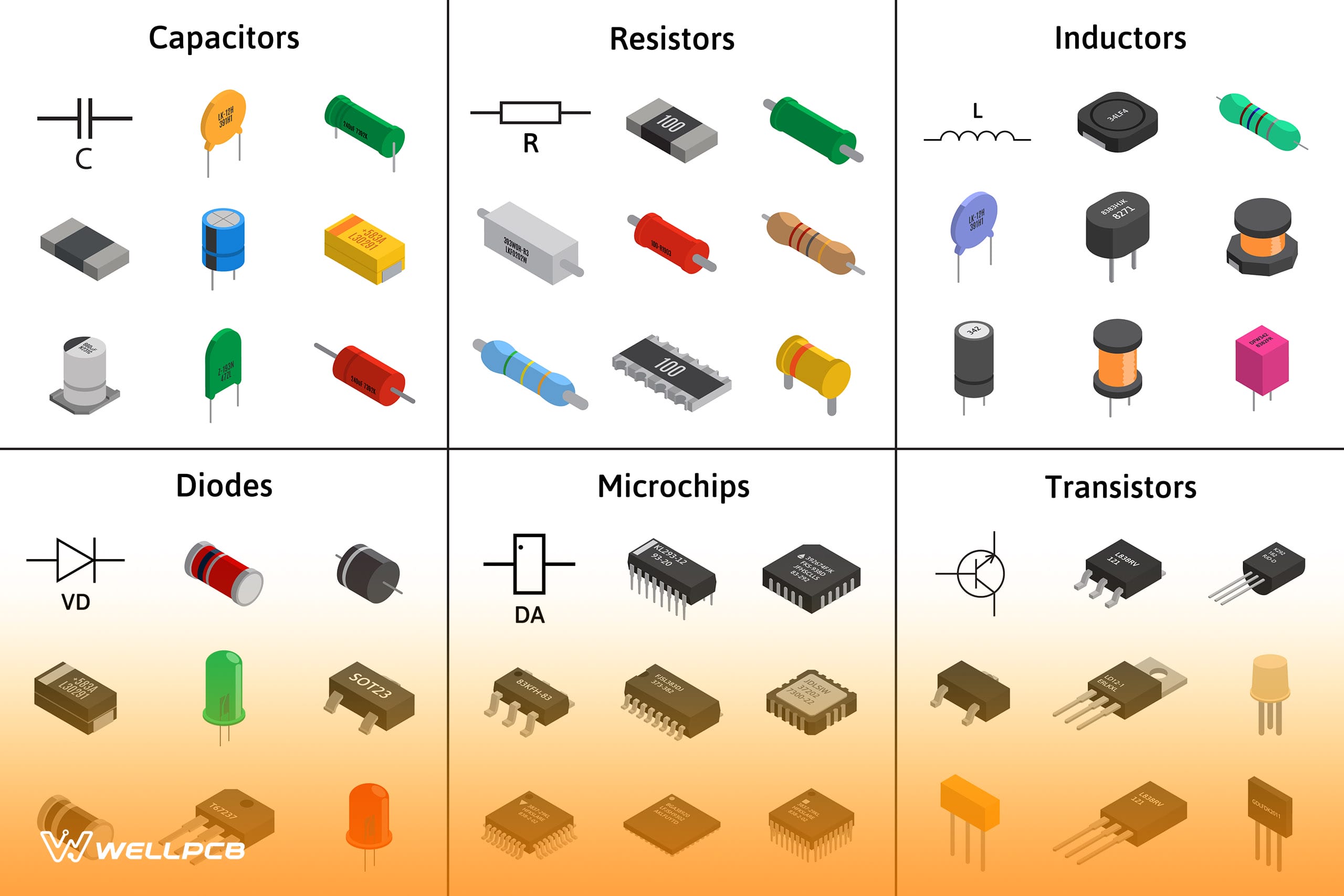
PCB Components Guide: Circuit Board Parts & Assembly
Without the various types of printed circuit boards (PCBs), many modern electronic devices would not exist. Whether it’s your phone, fridge, or televi...
7 Differences Between FR-4 and Rogers Material
As you may know, printed circuit boards play an essential role in nearly all electronic products that we use daily.
Therefore, you need to keep the ri...
How to Choose from 6 Types of Printed Circuit Boards
Nowadays, the types of printed circuit boards are everywhere. We interact with many PCBs daily.
They have made our lives easier and advanced.
You ca...

The Ultimate Guide to Electronics Manufacturing You Need to Know
Being new to electronics manufacturing can be overwhelming. Numerous aspects of electronics manufacturing are vital to the existence of any electronic...

The Ultimate Guide to Designing Custom Circuit Boards
Every day, people depend heavily on electronic devices to get things done around the house and at their workplaces.
These devices help us cook, cle...
The Ultimate Guide to Saving Production with Batched PCBs
Every printed circuit board must perform a specific function for a specific project.
In Today’s technological world, you will observe that almost eve...
What You Should Know About Single-Sided and Double-Sided PCBs
Single-sided and Double-sided PCBis a matter of routine and design convenience at the cost of a more complicated manufacturing process. The following ...

What Is The PCB Thickness Standard?
PCB Thickness is the technology of PCB is not at a standstill; rather, it has been evolving from level to level and from one stage to another differen...

PCB Etching-Tips And Guides On Etching Your PCB
Right until now, have you been searching for the buried secrets behind PCB etching? You are indeed in the right place; we would take you through the l...
USB PCB-How To Solve The Problems You Will Face
Are you using USB connectors the right way? Like all other hardware, USB connectors are also prone to issues. Know about the different USB PCB problem...

PCB Vs. Motherboard: Are They Different?
For a less tech-savvy person, PCB vs. motherboard might be the same thing. It gets more complicated when you consider that both of them have evolved i...

DIY PCB Board for Beginners
While it takes a professional PCB manufacturer to produce quality printed circuit boards, you can create your very own homemade printed circuit board ...

Reducing PCB Cost –Top 7 Tips to Help Save Cost During PCB Manufacturing & Assembly
On Reducing PCB Cost: When buying electronic gadgets, it is always the aim of most buyers to check out cheaper and quality device alternatives.
Thus, ...

6 Truths You Need to Know About Bare PCB Manufacturing
The moment we think about printed circuit boards, we usually think about their designs in addition to the applications in real life. We could even thi...
Back Drill PCB: What It Is and How to Use It
PCB manufacturing and design come with various challenges that may affect operations and efficiency. And one problem you need to watch out for is reta...
Wirewound vs Metal Film Resistor: Which is Better?
The following explores wirewound vs metal film resistor. For those who are uninitiated, it may be surprising to discover that metal-based resistors te...
PCB Drill Sizes-A Remarkable Informative Introducing
A CNC drill machine with many drill heads can drill all the different hole sizes needed at a high rate.
Devices differ by speed, PCB Drill Sizes, an...
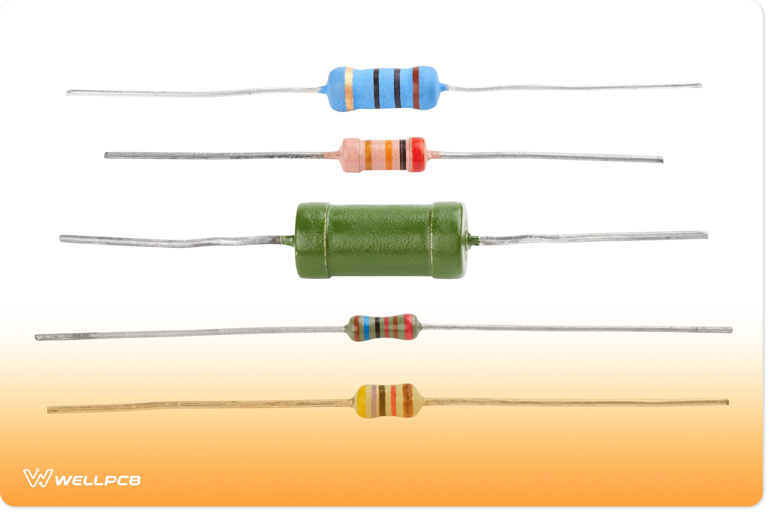
Carbon Film Resistor VS Metal Film – How to Tell the Difference
Resistors are electronic components that decrease electric current flow in circuits, thereby regulating electric current. Film resistors come in thre...

Helping You Optimize the Thermal Profile of Your PCB
People often underestimate the role PCB thermal simulation and analysis software has to play in the PCB design and manufacturing process.
The PCB’s...
Transparent PCB: The New Generation of Flexible Circuit Boards
A transparent PCB is revolutionary! This advanced technology changes how we view and use PCBs by offering enticing benefits. In truth, many LCD and LE...

PCB Overmold: What You Need to Know
Since PCBAs can sometimes be sensitive to environmental situations, you will mostly find them with a protective barrier. That's where the injection mo...
Polyimide PCB: Types, Applications, and Benefits
Most manufacturers produce their printed circuit boards with FR4 materials. After all, these boards are cheap and useful for various applications. But...
Black Pad: How to Avoid it on your PCB
Black pad is notorious for causing many PCB failures.
But most people don't suspect it when such situations occur.
In truth, a defective component ...
What is Flux & Why is it so Important?
"Flux" in the flux board is one of the most widely used words in the English dictionary. It can refer to the flow rate of particles, the amount of dis...
TQFP vs LQFP: Comprehensive Comparison of Quad Flat Packages
When working with PCB design or editing software, you may come across two similar-looking IC packages: Thin Quad Flat Package (TQFP) and Low-Profile Q...
IC Packaging: How Should We Choose Different Types of IC Packaging?
IC is one of the essential components of almost every technology, so it continues to grow extensively.
Do you happen to be working in the electronics...

PCB Panel Size: Complete Guide to Panelization Guidelines
PCB is a broad field. Thanks to the improvement in technology, manufacturers can now make minute components. These components go into various parts of...

PCB Temperature: A Guide to How to Manage High Temperatures
While the concept of the PCB has certain fundamentals in its design that have remained unchanged for a long time, a technology that affects PCBs have ...
FFC vs FPC: What’s The Difference Between FFC and FPC?
For a majority of people, especially those who are still new or getting into the world of electronic and printed circuit boards, it may be a little bi...
Masking PCB: How and Why It’s Done
Masking PCB (printed circuit boards) is crucial in the PCB manufacturing process.
But why?
The following guide will answer this question as we...

PCB Assembly Express-How To Get A Valuable Service
Providing PCB Assembly Express service delivery is essential in reducing the costs incurred and ensuring your clients’ desired turnaround time. You al...
Consumer Electronics Manufacturing Industry Overview
The Consumer Electronics manufacturing industry manufactures and distributes electronic items, including televisions, telephones, video cameras, alarm...

Flex PCB Manufacturer in China
Flexible Printed Circuit (FPC) uses a highly reliable and excellent flex PCB material of polyimide or polyester film. Its properties include high wiri...
PCB Manufacturer China: Useful Tips for Selecting One
When you plan to make an electronic device or gadget, you may be thinking of a permanent solution for the primary objective of the invention, i.e., ma...

10 Common PCB Quality Problems You Should Know
PCB assembly is much correlated to PCB's quality of PCB design and manufacturing as every PCB design engineer tends to place and route components acco...

The Most Detailed Introduction AOI Inspection(Latest)
AOI Inspection stands for Automated Optical Inspection systems, mainly used for PCB manufacturing, bare board inspection, board assembly, board rework...

One-Stop PCB Assembly Of WellPCB Introducing
The WellPCB can be considered a reliable PCB manufacturer at present. The WellPCB has up-to-date technology to make the best PCBs for you based on you...

PCB Holder for Easy Soldering(Latest)
It would help if you were frustrated when the crocodile chips held your PCB at a perfect angle bent at the last moment for soldering. You would also f...
How To Create A Simple Circuit Board Drawing
How to Create a Simple Circuit Board Drawing: Creating a simple circuit board drawing is easier if you have the right tools.
Firstly, you need to kno...

PCB Manufacturing Process(Simple and Useful)
Printed circuit boards (PCBs) are the backbone of electronics and are widely applied in manufacturing computational electronics, including various dig...
Prototype PCB-How To Make It
When hardware or firmware is built on, the manufacturers or employers ask to develop a hardware prototype.
Prototype PCB, an electronic product, from...
How to Clean Flux Off PCB: A Comprehensive Guide
How to clean the flux off PCB ( printed circuit board) after soldering has been a matter of debate among most designers.
While some technicians prefe...

Fast Acting Fuse: How It’s Different from a Time Delay Fuse?
Fuses are essential components in any electric circuit.
And they interrupt or stop overcurrent, which protects a system from severe damage.
One com...

Board Stiffener: What It Is and How to Use One
Various technological advancements make PCBs what they are today, and one such innovation is the board stiffener.
Printed circuit boards are essentia...

Daisy Chain Routing: What it is and How to Use It
What do you do when your wireless signal doesn’t reach the house?
Such situations can be annoying, especially when multiple devices need that conne...

LED splitter: Installing multiple strip lights into one source!
Are you attempting to install multiple LED light strips in a room but only have one electrical source? A few techniques can help you through that proj...

Is Plugging Your Vias Necessary?
Via holes are crucial aspects of PCBs that create electrical connections between a trace on one layer and another. But did you know you could close th...

AOI Test – What Is Automated Optical Inspection Test?
Modern PCBs are much more complex and smaller compared to older boards. Even simple PCBs have thousands of solder joints, which are potential sources ...
SMT vs SMD – Ultimate Guide to PCB Assembly Terms
PCB assembly technologies are getting more advanced as we work on ways to improve electronic circuitry efficiency. We’re seeing faster, more efficient...
What are AC and DC- What is the difference?
There exist two primary forms of electrical current- AC and DC. Both are cardinal in running electrical devices. But, to understand which power source...

ALU PCB- Aluminum Base PCB Features and Applications
Different materials are useful as the metal base layer in manufacturing Metal core printed circuit boards. Today, we'll explore PCBs featuring an alum...

94v0 Circuit Board Diagram- Key Features and Applications
Heat generation applications will also need advanced circuit boards that can withstand the temperature.
That is one of the critical applications of ...
THT vs. SMD – Which Is the Better PCB Assembly Process?
Modern PCB assembly technologies are more advanced than their predecessors. They’re faster, more efficient, maybe cheaper, and allow for miniature cir...
Digital Sensors Examples: All You Need to Know
One step in the measurement process often involves using electrical and electrochemical sensors. Generally, popular sensors are primarily in two categ...

7 Segment Display Pinout: Complete Guide to Pins
The 7-segment display is one of the conventional techniques in electronic display devices like digital clocks. So, how do 7-segment display pins funct...
PIC32 vs. STM32: Everything You Need To Know
The PIC and STM microcontroller families have dominated the MCU market for a while. They are high quality, with a wide range of options, excellent dig...
7812 Voltage Regulator IC: Pinout, Circuit & How to Use
Do you need a fixed voltage linear regulator that's easy to set up and use? Have you heard of the 78XX series of regulators? The 7812 IC is a great vo...
Types of Inverters- Inverter Classifications and Subcategories
Companies and households that require a constant power supply need inverters. We'll cover the different types of inverters and their wide range of app...

Night light circuit – 4 Types of Night Light Circuits
Switching the regular lighting circuit on and off is a simple undertaking. But how about a night light circuit that switches on after dark? Our articl...
Pcb Antipad: Should You Use It for Your Designs?
PCB signal integrity is a pretty sensitive concept. Therefore, you'd have to consider several factors to ensure your PCB retains its integrity. Among ...
Automatic day night on off switch – All you need to know
An automatic day-night on-off switch can be helpful for a myriad of purposes as street lights or a simple college project. Join us as we discuss how a...
Li-ion charger circuit- All You need to Know
Lithium-ion batteries' popularity is rising owing to their significant advantages over lead-acid batteries. However, a Li-ion charger circuit is diffe...

Resistive Touch Sensor: What It Is and How It Works
Resistive touch sensors were first introduced in the 1960s but didn't take off until the late 1990s.
Resistive touch sensor applications now includ...

Wireless Charger Circuits – A Comprehensive Guide
Wireless electrical power transfer has been around for nearly a century but is finding more use today. Mobile phone companies invest in technology and...

FM transmitter circuit diagram – Full Illustrations of Various Variations
The FM transmitter circuit diagram is pertinent to explaining how radio waves travel and the general principle of FM radios. Our article will give the...

How to Use an Oscilloscope – A Beginner’s Guide
Oscilloscopes are essential for engineers as they aid in accurately measuring voltage waves. They enable you to see how circuit voltage changes over t...
1n4002 diode- All you need to Know
There are several general-purpose diodes on the market, and the 1N4002 diode is one of them. Join us as we explore the critical properties of the 1N40...

Micro SD Pinout- Secure Digital Memory Cards Guide
Conventional storage card types were extensive but stored relatively more secondary data than today's.
With everyday technological improvements, the...

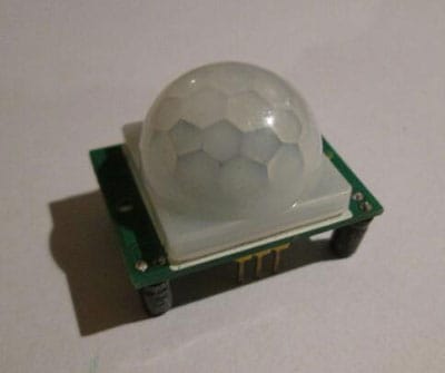
Motion Sensors Circuits – 5 DIY Ways of Building a Motion Detector
There are several ways you can detect motion or movement. Some of them include vibrations, sounds, and infrared light. Today, we'll discuss one means...
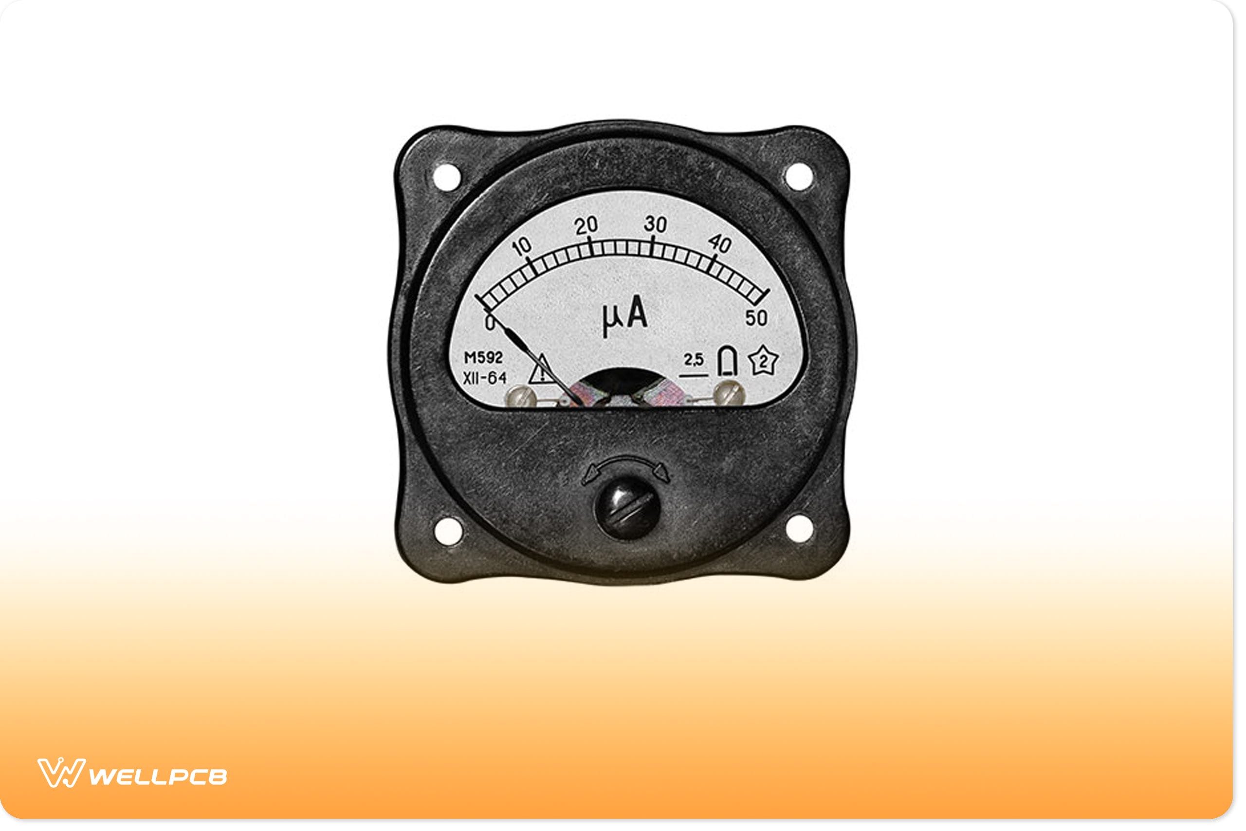
Micro amp Meter – Basic Working Principle
A multimeter is essentially the most common current meter. However, the device is unsuited for the measurement of small current levels. Thus, the micr...

NiMH Battery Charger Circuit – Features, Charging, and Working
NiMH batteries have higher energy densities, have 30 percent more capacity than NiCad batteries, and are environmentally friendly. However, most peopl...
FR1 PCB: How is it different from FR2, FR3, and FR4 PCBs
Flame Retardant (FR) materials are one of the many necessary materials that make up a PCB. Interestingly, they have up to four variants ranging from F...

DIY Remote Control: How to Build One Easily
Are you tired of dealing with remotes that don’t have as much function as you need? Well, a quick fix is to build a DIY remote control.
With this dev...
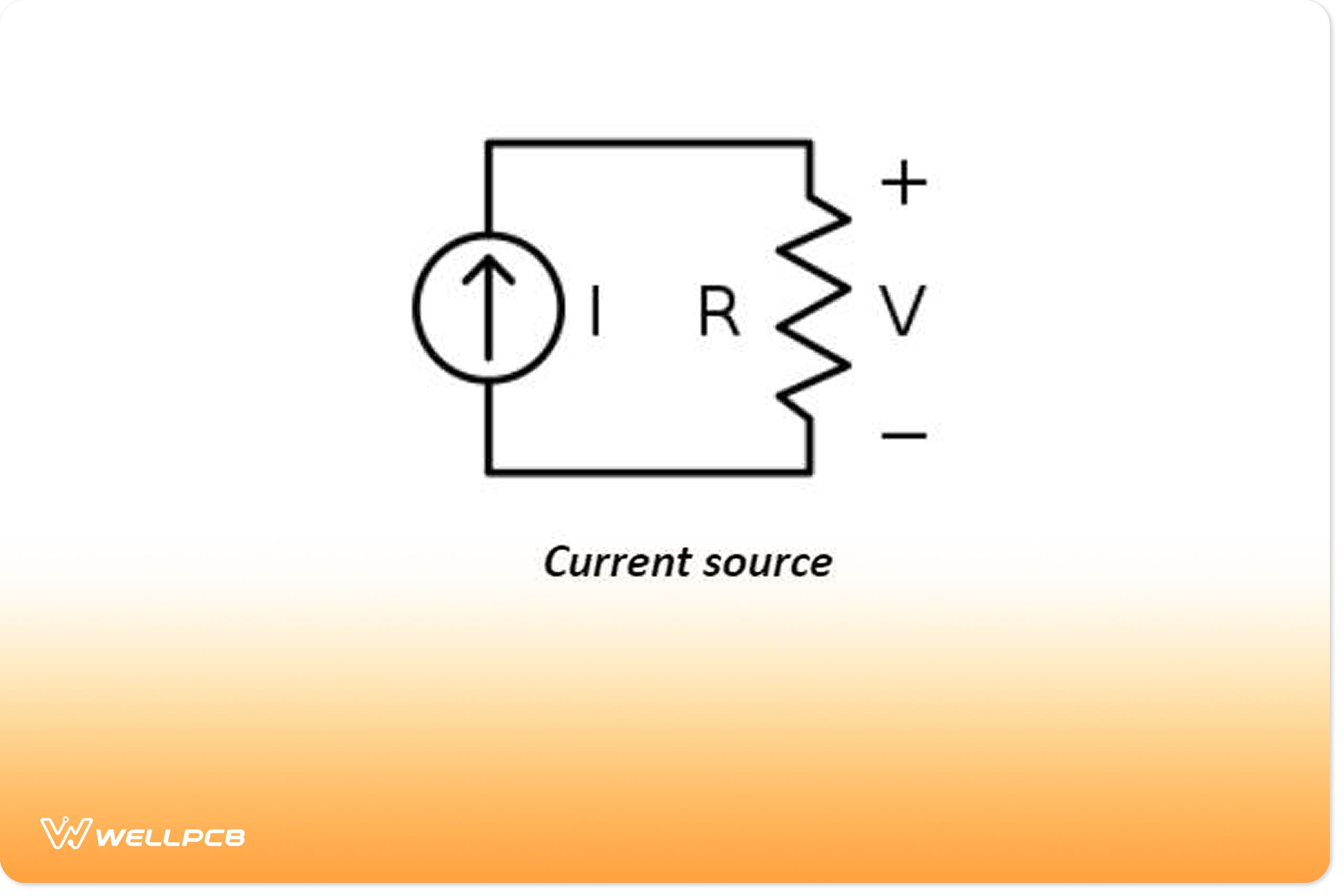
Constant Current Source – A Comprehensive Guide on Constructing Different Constant Current Circuit Designs
Electronic devices require a constant current supply that encounters zero to fewer interruptions. We also have several electronic circuit designs, lik...
Capacitor Polarity: How to Tell if It’s Polarized or Not
A variety of capacitors form part of electronic components in a circuit board. They function to store energy in electric form after you charge it and ...
10 Layer PCB Manufacturer: How to Choose the Right One for Your Project
If you are looking for a 10-layer PCB manufacturer, you have come to the right place. In this blog post, we will discuss how to choose the right one f...
Double Throw Relay: SPDT & DPDT Wiring Diagrams Explained
Relays are essential to control devices that we can interface with Arduino and Raspberry Pi boards for control.
They're beneficial as they eliminate...

Embedded PCB: The Perfect Board for Embedded Systems
There’s a steady increase in sales of embedded systems due to the high demand for smaller, wearable circuits. In addition, embedded systems help to cr...

Interfacing PN532 with Arduino – Here’s All You Need to Know
About interfacing PN532 with arduino, PN532 is an NFC breakout board found in almost all devices using near-field communication. And as NFC is an exte...
Copper Clad PCB – What Is Copper Clad Laminate (CCL)?
There is an increasing demand for thin and ultralight electronic components. As a result, this pushes manufacturers to find a circuit board featuring ...

OSP PCB: An Effective PCB Surface Finish
Do you know what happens to copper when exposed to atmospheric moisture? It oxidizes quickly and may lose all its properties. The same thing applies t...

Microwave PCB: The Best PCB Design for High Frequencies
It's a common fact that standard PCB designs can't handle everything. You will need some specialized techniques to pull off some demanding application...

8 Layer PCB Manufacturer– Everything You Need to Know
If you are looking for an 8 layer PCB manufacturer, you have come to the right place. In this blog post, we will discuss everything you need to know a...

Bluetooth Communication Protocol – The Ultimate Protocol Guide for Learners
Generally, Bluetooth communication protocol, a Bluetooth network technology, provides wireless communication between mobile devices over a short-range...

Arduino Pro Mini vs Nano – A Comprehensive Comparison
The Arduino board is one of the most popular microcontrollers due to its versatility. Often, many people opt for the Arduino Uno, but where fitting in...

PCB Designs: A Comprehensive Guide to Basic Design Steps and Rules
A circuit board designing process involves time-demanding steps that should follow to the maximum. Failure to adhere to the instructions often costs P...

High Current PCB: The Perfect Board for High Current Applications
Let’s face it! It’s frustrating to see your circuit explode or malfunction, mainly because it can’t handle the current requirements of specific applic...

433MHz: An All-Inclusive Guide to the Wireless Radio Band
Wireless communication enables information transfer from one point to another without using a transfer medium like an electrical conductor. An example...
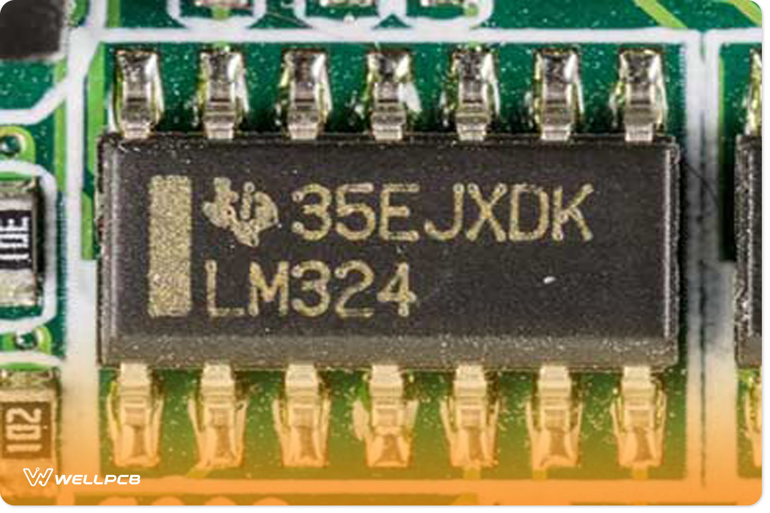
LM324 Circuits: Different Circuits You Can Make with the LM324
Have you ever come across the LM324 circuit diagrams before? If yes, you should know it’s common to find in different courses because of its operation...
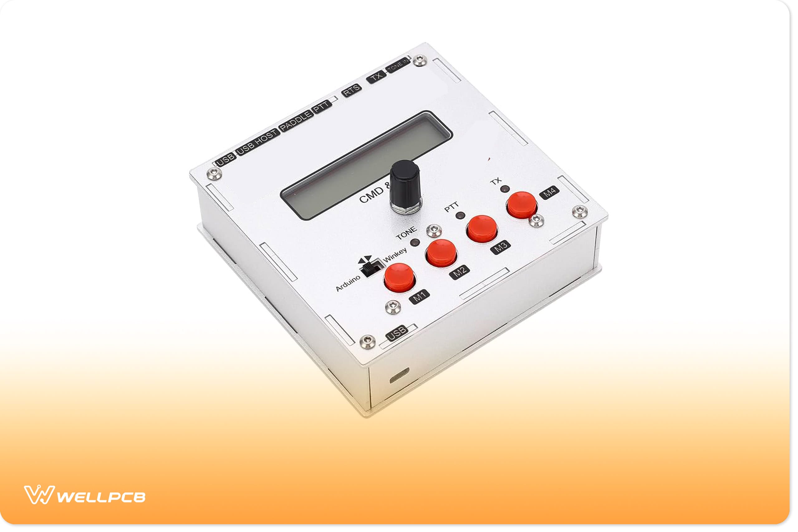
k3ng Keyer: Explanation on the Arduino bases Morse Code
A keyer is a piece of equipment that allows signaling by hand via pressing a single or more switches. For example, we have a keyer in a telegraph key ...

Atmega328p vs Atmega328- Features, Differences, and Similarities
When buying a microprocessor, you need to go for the particular one that solves your needs. We have prepared this article to help you differentiate be...

PCB Track Width: How to Calculate and Optimize PCB Trace Width
If you’ve worked with PCBs, you’ve likely noticed the copper tracks connecting different points. But have you ever wondered whether their thickness ma...
Temperature Controller Circuit: What Makes it Tick?
Control applications offer a lot of project ideas. But, in truth, you can control various devices and appliances with the right circuit. So, perhaps, ...
IR2104: Understanding All About This MOSFET Driver
Several homes and industry appliances depend on semiconductor integrated circuits. They use an H-bridge to drive loads from low-power input to produce...
Platform IO: The Ecosystem Every High-level Professional Needs
Have you been doing a lot of development in Arduino and Arduino IDE? But you’re getting a bit frustrated with the limitations of Arduino when you need...
LM311 Equivalent: The Ultimate Guide
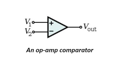
Differential comparators are electronic devices that compare two currents or voltages before outputting a more excellent digital signal. They mostly h...
AT89c51 Microcontroller: Programming, Pinout, Features, and Alternatives
Atmel AT89 series fall under the 8-bit microcontroller family compatible with Intel 8051. Their advantages include cost-effectiveness and high flexibi...
DS18B20 1-Wire Digital Temperature Sensor – Pinout, Features, and Applications
Digital sensors convert and transmit data digitally, examples being pressure, humidity, and temperature sensors. The DS18B20 temperature sensor is one...
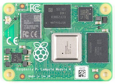
Compute Module: What It Is and Why You Need the Board
Are you looking for an available module to develop a sellable product that fits into a standard SODIMM connector? Then, a compute module is what you n...

TTL vs rs232- Differences, Upsides, and Downsides
The Serial communication method is one of the most reliable data transmission modes over long distances. We will expound on the two main protocols in ...
6 Layer PCB Manufacturer With Stack up Types
Are you in the market for a 6-layer PCB manufacturer?
If so, you're in luck! This blog post will introduce some of the best 6-layer PCB manufacturer...

Rk3399: Everything You Need to Know About It
Are you looking for a different option other than Raspberry Pi or Adafruit SBCs? Or do you need a fantastic alternative for your mini-computing needs?...

DIY Thermal Imaging Camera: How to build a Less-Expensive One
Are you looking for a way to capture heat signatures during winter but can't afford any of the commercial thermal cameras? If yes, what you need is a ...

Ipfire vs Pfsense: Which Firewall Should You Choose?
Are you an engineer or designer looking for the best firewall and stuck between IPfire vs PFsense?
Then you’re in the right place.
Indeed, IPfi...
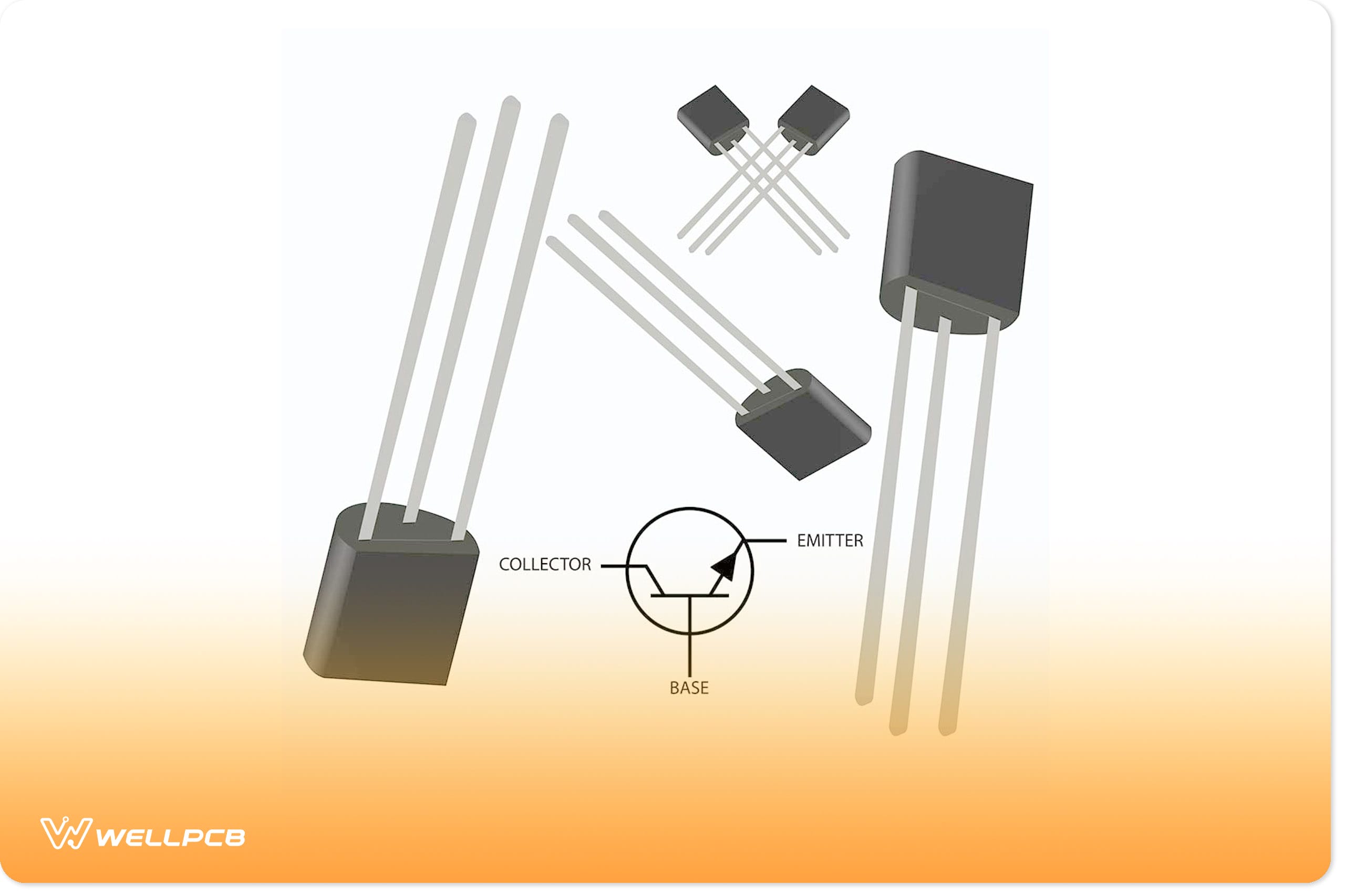
Transistor Types: A Complete Guide to All Transistors
Electronic circuits incorporate various components to facilitate effective functioning. Among these components are transistors that come in a wide ran...

AD9850 Module: A detailed Guide
A signal generator is an electronic device that generates signals showing different features, thus very handy electrical equipment. One such generator...
Arduino Speaker: How to Build an Easy One
Are you looking for unique projects to build with your Arduino? Then, you can make an Arduino speaker. The Arduino speaker is a musical project you ca...

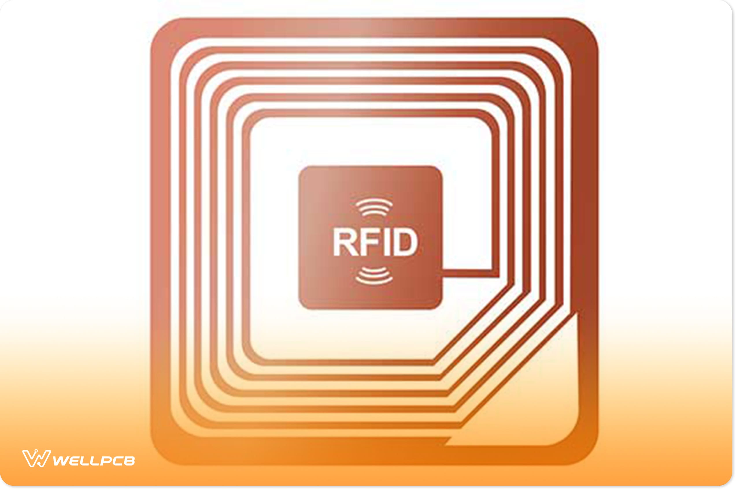
NFC Antenna: What it is and How it Works
Do you need an NFC antenna for your circuit project? But you don't understand how it works. If yes, you're reading the right article.
In truth, NFC ...
Colpitts Oscillator: Circuit Application and Its Advantages
The Colpitts oscillator is a linear oscillator and just one among many LC oscillators. Importantly, this oscillator uses the functioning unity of capa...
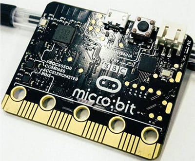
Micro: Bit Projects: 11 Cool Projects for Beginners
Are you a beginner looking for the perfect microcontroller for your programming needs? What you need is a Micro: bit Projects.
In truth, there are ma...

Motionless Electromagnetic Generator: A Guide on Designing a MEG Circuit
An electric generator is an electric device converting mechanical energy/motive power into electric power that drives an external circuit. There are s...
CH304G: The Features, Applications, and Schematic
Are you looking for an affordable chip that allows you to interface a USB port with microcontrollers easily? Then, what you need is the CH340G.
Not...
Microwave Sensor: What It Is, Types, & the Working Principle
Let's face it! Security has become a thing of worry these days. Thus, motion sensors are one of the best ways to protect vulnerable points. Interestin...

NOOBS vs Raspbian: What Are the Major Differences Between Them?
Are you running a Raspberry Pi project, and you're confused about whether to choose a NOOBS vs Raspbian OS? If yes, we're here to help you!
Installin...
Attiny84 Datasheet: Its Pin Configuration and Programming Steps
Attiny84 is a single chip with high performance but uses low power. The device is based on an advanced RISC architecture. Also, this microcontroller i...

CD4012: Why This Logic Gate IC is Unique
In our daily lives, digital communication has come to play an important part. The Motorola CD4012, for example, is playing a vital role in solving the...
Uln2003 pinout: A Comprehensive Guide on ULN2003 IC Datasheet
Minimizing and controlling high-voltage circuits in DC devices is challenging. The solution offered previously was using high-voltage DC motors becaus...

Flexible VS Rigid: The Differences in the Circuit Board Assemblies
Printed circuit boards (PCBs) are layout data devices that connect electronic components in several non-consumer and consumer devices. Therefore, depe...
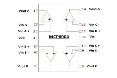
MCP6004 Datasheet – A Look Into the Low Power Quad Op-Amp
An operational amplifier (Op-Amp) is an electronic device that works with external components like resistors and capacitors to amplify voltage. There...
CD4027- A Complete User Guide
In electronics, there are many devices that you can use for data storage. However, none does it better than the high-speed CD4027 Dual JK Flip-Flop th...

Hc06 Datasheet: Introduction to Pinout, Features, Applications, and Working Principle
Bluetooth is a wireless technology that uses radio frequencies or waves to exchange data with different devices. Further, you can see its operation in...
Light Detecting Circuits: An Easy Way to Detect Light
Are you looking to build a project that detects the presence and absence of light? Then, it would help if you had a light-detecting circuit. Interesti...
CD4013: Basic Guide on Pinout, Application Circuit
Dual or D-type flip-flops are circuits that store data in a 1-bit form and have high or low output data. Also, its output changes to the D/ data input...

Gerber Files: What They Are and How to Create Them
Have you heard of schematic capture programs that generate Gerber files, but you have no clue how it works? Or are you dealing with PCB projects and n...
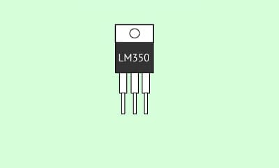
LM350 – A Complete Guide on Voltage Regulation
A voltage regulator keeps the output voltage constant regardless of the input or load conditions or changes. One easy-to-use but very effective voltag...

Capacitive Voltage Divider: An In-depth Guide
Capacitive voltage dividers have increasingly grown in popularity; you will find them used in many electrical projects such as Colpitts oscillators, a...

Buzzer Datasheet: A Detailed Explanation
A buzzer is a practical sound feature used in various electronic devices and applications. It is a small 2-pin component that can fit on a breadboard....
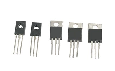
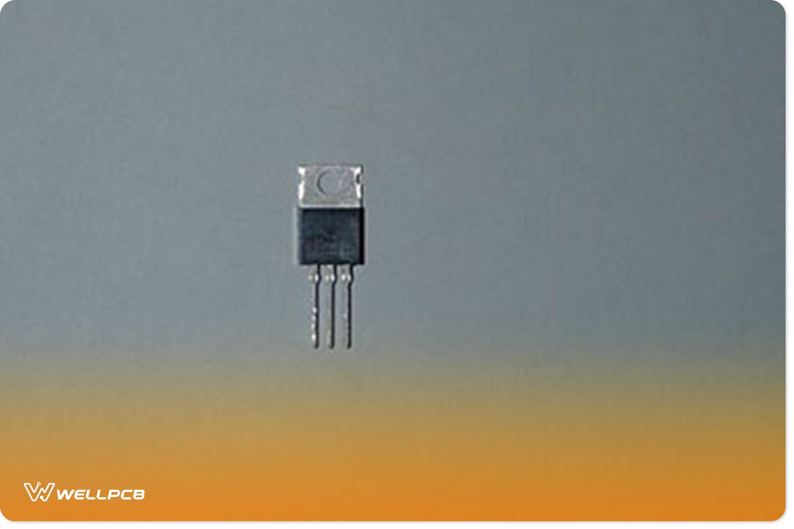
TIP31C Pinout: Technical Knowledge of the NPN Transistor
About TIP31C Pinout, Negative-Positive-Negative (NPN) power transistors, under bipolar junction transistors, amplify signals or circuit applications a...
LM7805 Circuit: Voltage Regulator IC Overview
Electronic circuits sometimes require a stable power supply to function harmoniously with other components.
However, the power supply is not always c...

Beat Frequency Oscillator- Principle and Applications
An oscillator capable of producing a variable output frequency signal is essential in electronics. The beat frequency oscillator is among the best sui...
TDA2822- A Complete Guide
Operational amplifiers (Op-Amps) play a crucial part in amplifying electrical signals in electronic circuits. An op-amp amplifies the signal producing...

LM1875: A Comprehensive Guide on Audio Amplification
As per the name, an audio power amplifier amplifies audio signals to high levels that can drive headphones or loudspeakers. An example is LM1875 IC (f...
HT12D: A Guide on an RF Decoder IC for Remote Control Applications
HT12D Integrated Circuit is a 212 decoder falling under a series of CMOS LSIs. The 18-pin decoder is applicable in remote control systems. Further on,...
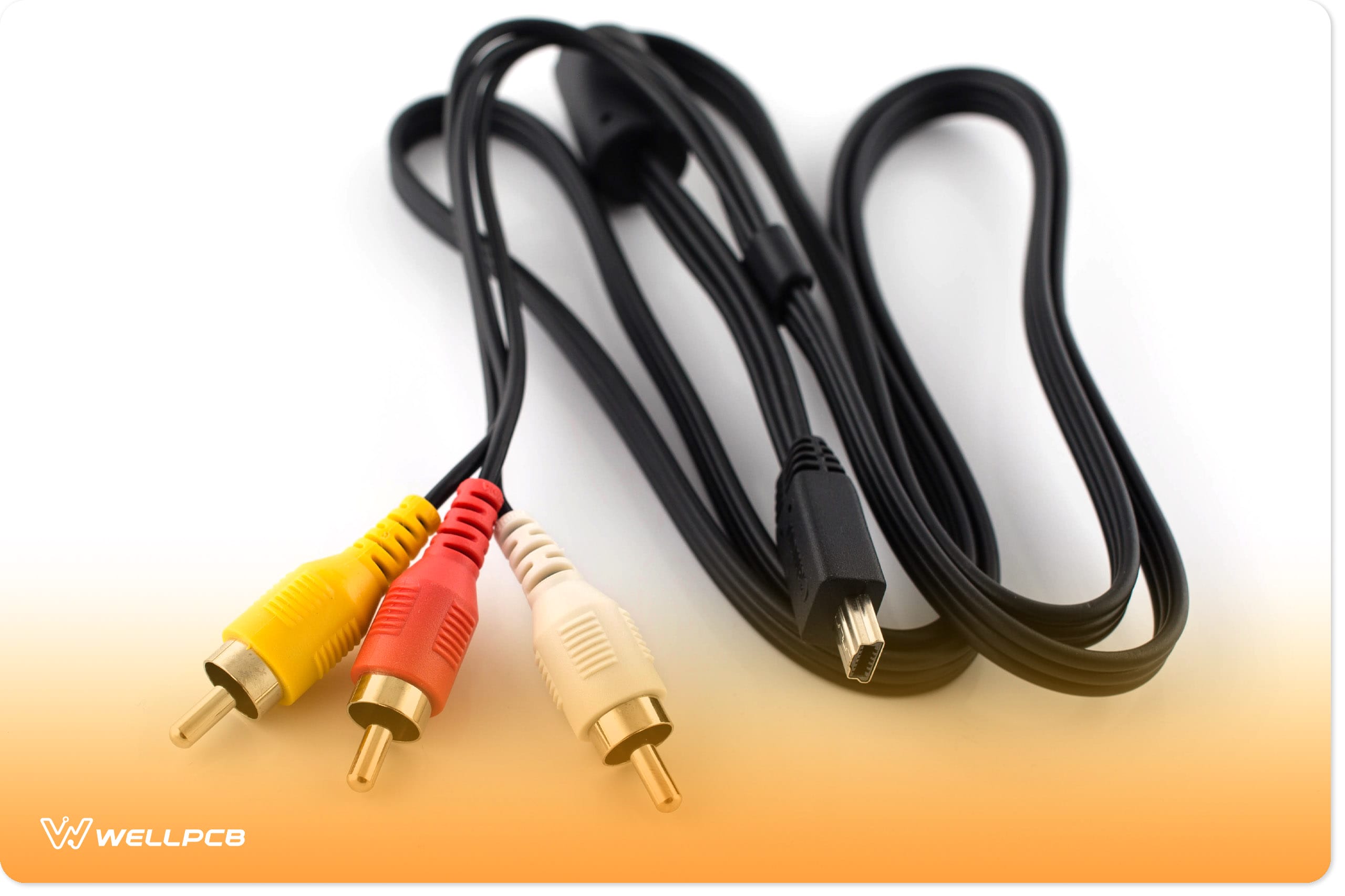
S-Video to RCA Cables: Getting the Most Out of Your Connections
Have you noticed how the cables connecting your DVD player to your TV have changed over the years? Just as technology evolves, so do the tools we use ...
Tip122 Pinout: Guide to What It is, Features, and How to Use It
The TIP122 pinout is a Darlington power transistor. A Darlington power transistor means that a transistor pair is in one box. Importantly, the main re...
7815 voltage regulator: Detailed Guide on How to Use It And More!
Voltage regulators are very popular in electrical projects. They work by providing a sustained output voltage despite the feed-in voltage presented. T...

Push Button Switch Wiring: What It Is, Features, Types, How It Works, And Applications
Do you need a simple way to control your circuits or piece of machinery? Then, a pushbutton switch wiring is what you need.
Push-button switches can ...
BC547: Transistor Explained
If you're an electric enthusiast, the chances are that you'll come across a BC547 in one way another.
Here, we will be discussing all that there is ...
DMOS Transistor: Its Capabilities and Structures Explained
The double-diffusion DMOS transistor work wonders in electrical circuits that more folks need to understand. The transistor is a master key in brake c...
AGC Circuit: A Comprehensive Overview
The Automatic Gain Control (AGC) helps solve signal input and output problems, specifically fluctuating signals. That much you already know; however, ...
BJT Biasing: Everything You Need to Know
Electronic circuits with amplification capabilities can perform more efficiently if the BJT undergoes biasing. Generally, this process involves applyi...

BC558 Transistor: Everything You Need to Know
Transistors are electronic components that operate by switching or amplifying the power and electric input signals. Therefore, in applying current or ...
LM335 Temperature Sensor: Configuration, Specifications, and Applications
Many different temperature sensors use different measuring principles and technologies to achieve a measurement. Some work best in certain conditions,...
CD4066: Features, Working Principle, and Applications
CMOS (Complementary metal-oxide-semiconductor) is a MOSFET type using symmetrical and complementary pairs of n-and p-type MOSFETs in logic functioning...

Mg996r: A Brief Introduction into Its Working and Applications
A motor is an electronic device capable of converting electrical to mechanical energy. There are several kinds of motors in the market. These include ...
Silicon Circuit Board: Benefits and How to Design One
Why should you use a silicon circuit board? Simple, Si, or silicon is a simple element with unique features. Also, it acts as an insulator and conduct...
Phone Circuit: The Basic Components and How It Works
If you make a list of the most important electronic devices in people's lives, it's almost impossible to miss a cell phone. Why? Mobile phones are one...
LM7824: Description, Specs, Applications, Pinout
Generally, voltage regulators are electronic components that are common in the majority of electric circuits. They generate a constant output voltage ...
Sg3524 Modulator IC: Pin Configuration, Specifications, And its Application
Knowledge or enthusiasm for electronics might have brought the SG3524 inverter chip to your attention. SG3524 chip is one of the most critical compone...

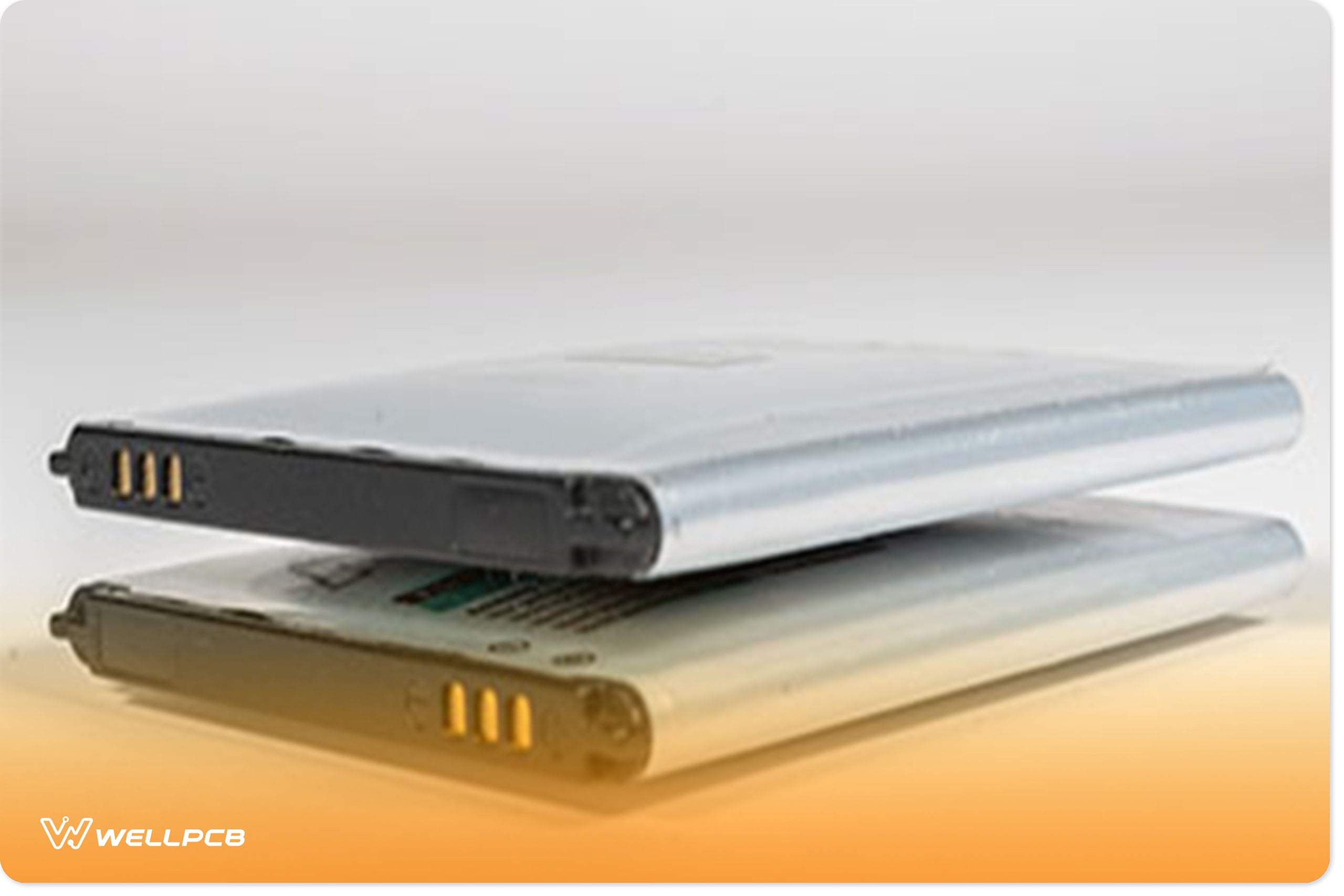
2600mAh Battery: Working, Specifications, Application Circuit, and Other Useful Knowledge
A Li-ion battery/ Li-ion battery is a rechargeable battery whereby lithium ions move from a negative to a positive electrode. The medium is a battery ...

CD4060: Ultimate Guide for its Circuits, Operation, and More!
The CD4060 is an integrated circuit that belongs to the CD4000 series of integrated circuits. It contains an in-built oscillator that has the power to...

Cold Electricity: Ultimate Guide on the Basics
Cold electricity is electricity generated through an opposing line of the LC network. The unconventional principle governing its production first ensu...
LM723 Circuit: A Detailed Information on the Voltage Regulator
There's no doubt that you've come across several types of voltage regulators, like 7805, 7812, etc., that regulate power supplies. While they are effe...

1n4148 Diode Equivalent- All You Need to Know
In electronic circuits, the unidirectional flow of electric current perspective is very significant. Also, the electronic component responsible for su...
Different Types of Solder- All Common Classifications
When making electrical connections, one of the most critical aspects is soldering. Also, the soldering process is inevitable in joining almost all ele...
Types of DAC: Basics on Digital to Analog Converter ICS
Signals are generally classified into major groups, digital signal and analog signal. And for each call, there are different types of applications. Fo...
UC3844: A Complete Guide to Everything you Need to Know
Signals are generally classified into major groups, digital signal and analog signal. And for each call, there are different types of applications. Fo...

DTV Antennas: Types, Installation, and How to Make One
Are you stuck with an expensive TV subscription over a coaxial cable or satellite dish? And you need a more convenient solution?
Well, the good new...
QFN Packaging: Types, Assembly, and Benefits
Do you deal with microcomputers, PCBs, or programmable modules? Then, you need an IC component that works. And the QFN or quad micro lead frame packag...
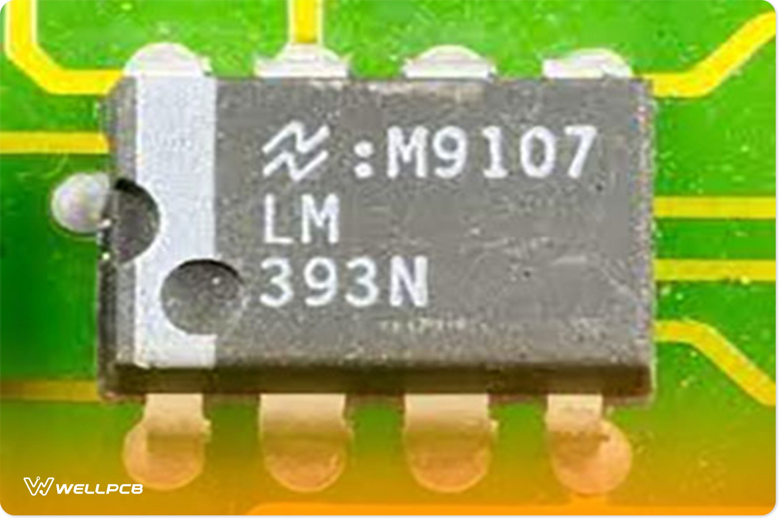
LM393 Comparator IC: Pinout, Working, and Applications Guide
A voltage comparator is an electronic component that compares two currents or voltages and then determines which is greater at the output.
General...
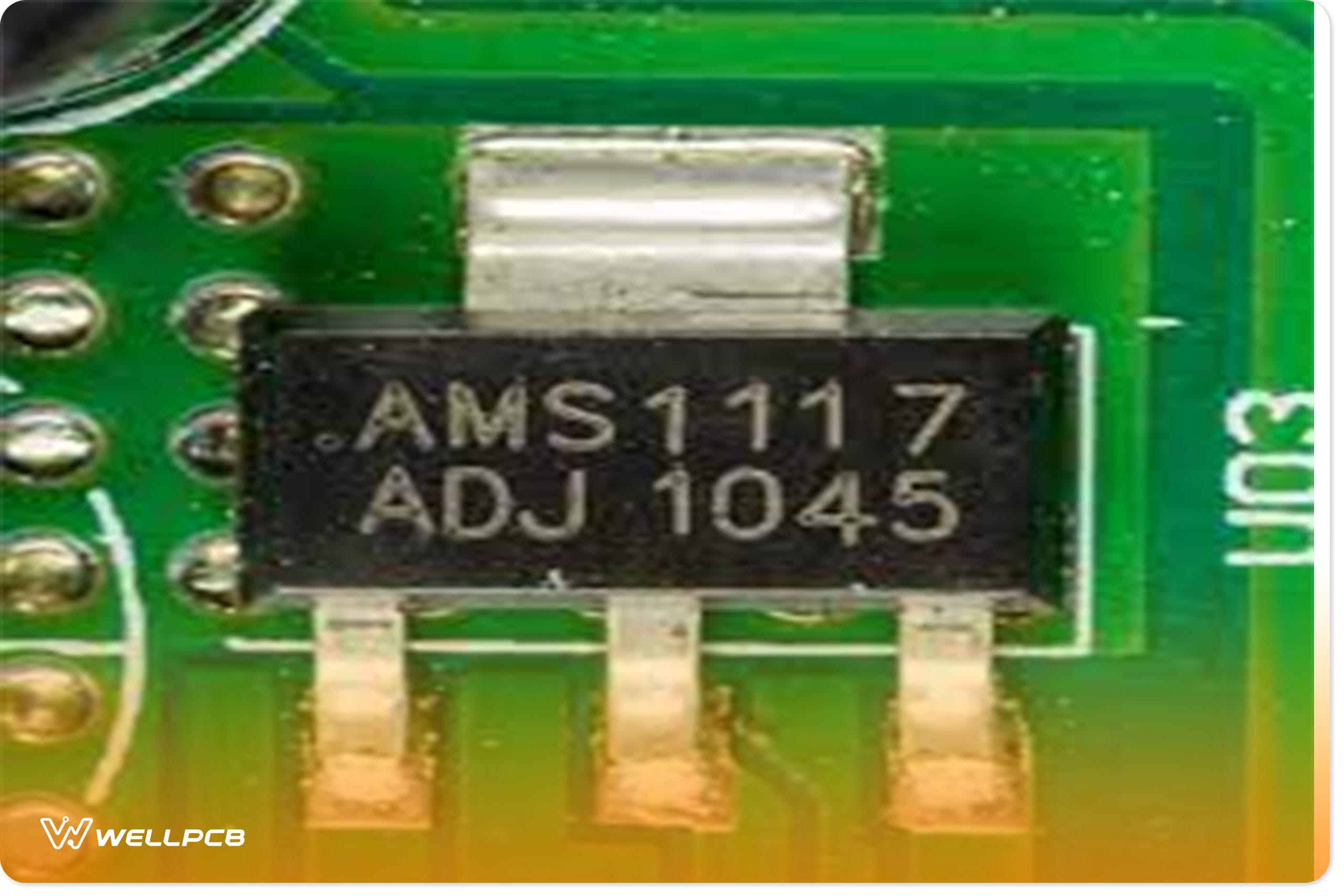
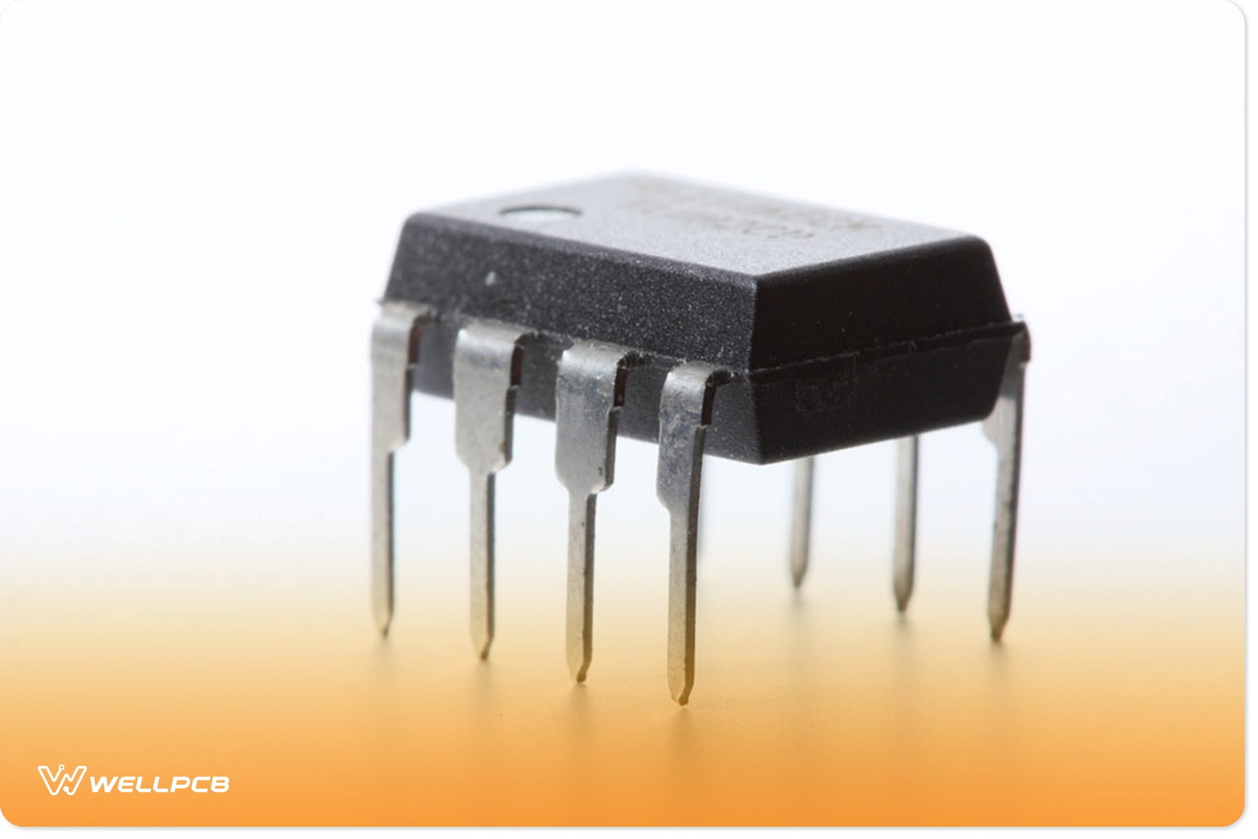
AMS1117 Pinout: Beginner’s Guide to Circuit & Connections
AMS1117 Pinout is a linear voltage regulator, often available as an SMD component or DCY package.
The 3-pin device has variable/ adjustable and fi...

AM Receiver Circuit: Understanding and Building A Simple Project with It
Have you ever used a walkie-talkie or an audio amplifier? Or are you into radio listening as a hobby, switching from one FM/AM band to the other? For ...
Center-Tapped Transformers: A Brief Introduction into Its Working and Applications
Whether working on a rectifier circuit or powering your home, a center-tapped transformer or center-tap transformer is convenient.
Hence, we look at...
IRFZ44N MOSFET: Complete Guide to Specs, Circuits & Uses
We all agree that transistors have taken newer shapes and specifications since their invention. Talk about the BJT and MOSFET transistors. These are m...

Crystal Oscillator Circuit: How to Build One
Are you an engineer or manufacturer who wants to understand the frequency of tracking time or stabilizing radio transmitters and receivers? If yes, yo...
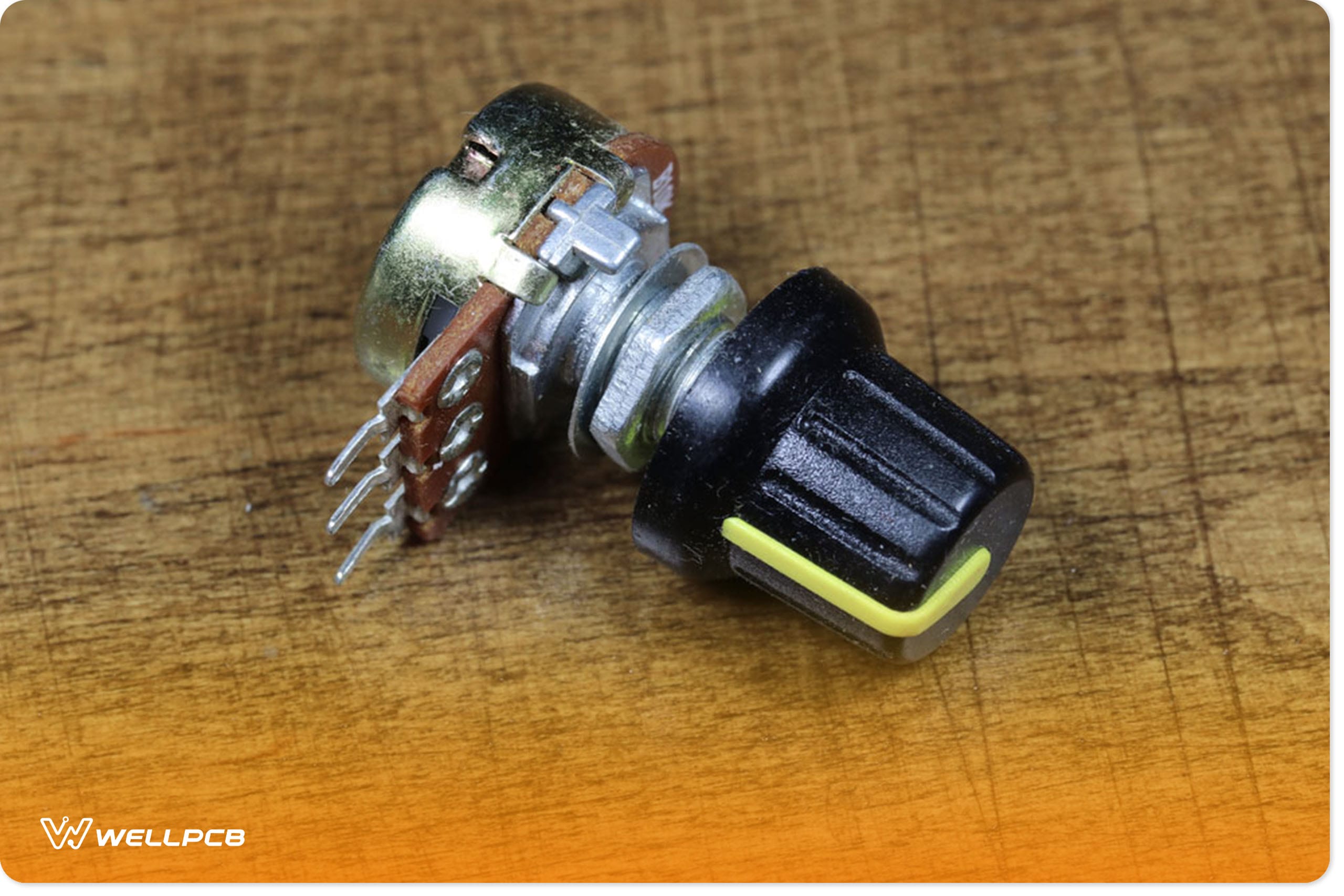
Potentiometer Wiring – Process Simplified
When operating a radio or a musical instrument, you turn a button for volume controls.
Also, if you've interacted with an audio amplifier, you might...
SCR Bt151: A Complete Manual Guide
Nowadays, microelectronic components are vital in circuits. Most are improved versions of the basic ones. Examples include resistors, capacitors, indu...

X Rated Capacitor: How to Use One in a Transformerless Power Supply
Capacitors are the holy grail of electronics. After all, you can find these electronic components in LED lighting, signal processing, power supply, co...

Yagi Antenna Design Formula: Understanding its Parasitic Elements and More!
An antenna is a device used to transmit or receive electronic signals. All devices that use frequency radiation use antennas.
We have very many diff...

Brushless Motor Wiring: Its Specifications and Complete Guide!
We can compare a BLDC motor to a brushed motor wiring, but not entirely. A brushless motor is a three-wire motor that we can use in electrical devices...

Emitter Follower Circuit: The Basics and How to Create One
Does your electronics project require impedance matching? Or do you need a circuit with a transistor that can pull a little current from the input? In...
Start Stop Circuits- A Brief Introduction Into Its Components, Working, And Control
The Industrial Revolution and the ever-changing engineering scope created more extensive and complex systems.
And for such systems, human safety and...
Low Voltage Cutoff Circuit: The Working Principle and How to Make One
If you can care for and use your rechargeable batteries correctly, they can last for at least two years. Thus, taking care of your rechargeable batter...
Blocking Oscillators: An Introduction Into its Working, Types, and Uses
You may be doing a project that requires you to know about blocking oscillators. Do you have worries that it might overwhelm you?
Blocking or puls...
2SC2879: Everything you Need to Know and More!
One of the most original transistors in the transistor family is the 2sc2879. It is one of the most popular frequency transistors because of its use i...
Overvoltage Protection Circuit: Meaning, Types, and DIY Projects Explained
Undeniably, you must have experienced or heard of an overvoltage condition occurring due to, for example, faults in the supply. You might have also se...
Battery Backup Circuit: A Comprehensive Guide in Making One
There's a high chance you've experienced a power outage but automatically got another battery power. Backup batteries generally supply power to a syst...

Speaker Crossover Wiring Diagram: The Types and How to Build the Network Circuit
Can a hi-fi system alongside a loudspeaker give you a complete system? Well, that’s true until you notice different frequencies flying around your spa...
Water Detector Circuit- Working Principle and Basics
If you own a fish pond or a swimming pool, you understand how a water leak can be frustrating. It'll prompt you to keep refilling the water, which is ...

Notch Filter Design: A Narrow Band Filter for Specific Noise Attenuation
Noise and interference are common when dealing with electrical devices because different circuits produce varying signal frequencies that clash. Such ...
Electronic Circuits for Beginners: The Complete Guide
An electronic circuit is simply a path for electrons. Circuits are passages for electric current to flow. Hence, the bulb needs a closed path for the ...

Homemade Car Alarm: The Benefits and How to Make the Device
Did you know that the United States alone experienced a hike in the national rate of motor vehicle theft within the last 30 years? This report from St...

RGB LED Controller Circuit: The Working Principle and How to Make One
Do you fancy stage lighting designs, LED matrix displays, 3D billboard lights, outdoor decoration lighting, and other lighting designs? And you plan t...
Relay Drive; Definition, Working Principle, and Application Circuits
A relay drive is an electronic component you'll encounter in numerous electronic circuits and electrical devices. The different relay types particular...
Dpdt Relay: The Complete Guide
A relay is a switch with an electrical circuit operating it. Since it is a circuit, it has a series of input signals and control signals. Significantl...

Metal Detector Circuit: An Introduction Guide
Security is one of the few things that is a priority regardless of where you are in the world. As a result, security check-in in most public and priva...

Voltage Doubler: A Cheaper and Lighter Alternative to Transformer-Rectifier Circuits
Are you thinking of building a high DC voltage test equipment? Such a device is necessary for testing or building electronics and appliances that requ...

Input Impedance of Op Amp: What It Is and How to Calculate It
First off, let's be clear: Op-Amp means operational amplifier. And the device is a high-gain electronic voltage amplifier (DC-coupled). Plus, it has a...
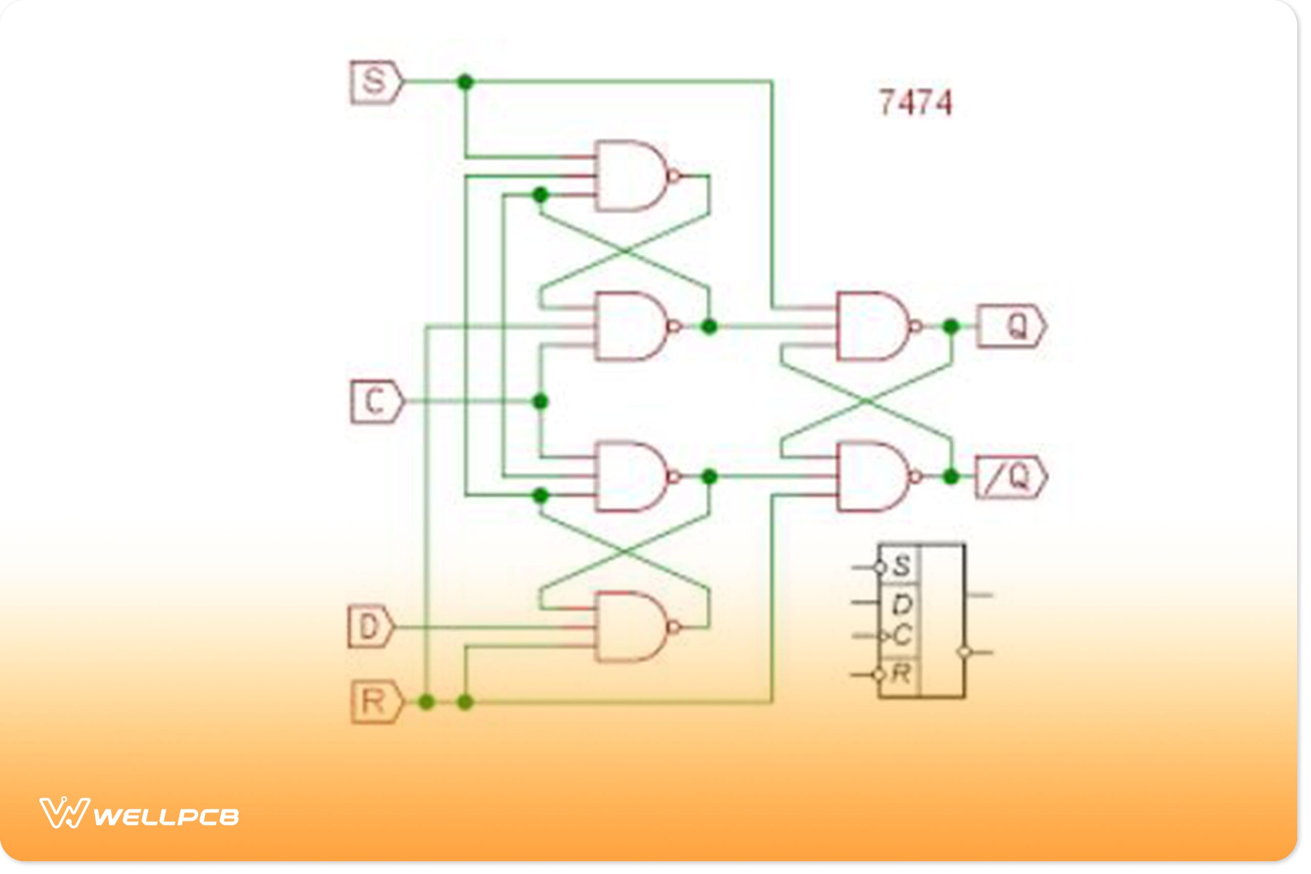
Negative Edge Triggered Flip-Flops: Basic Electronic Knowledge
Flip-flops or latch circuits majorly help to design registers and counters that store data in a multi-bit number form. However, the register devices o...
4047 IC: A Detailed Introduction To A Monostable and Astable Multivibrator
We will investigate the 4047 IC to keep you updated with impactful information on technology and engineering.
The 4047 IC is one of the most popular...

Log Amplifier – All Important Information to Know
High dynamic signals will always pose a problem to designers. They are necessary for echo-ranging devices such as radar or sonar systems. But in such ...
LM338 Circuit: Detailed Datasheet and Application Circuits
An LM338 integrated circuit is part of the LM-series ICs made by the National Semiconductor. LM338 application circuit is similar to LM350 or LM317 in...
Transistor Flip Flop: A Sequential Logic Circuit for Storing Binary Data
Are you interested in learning or making digital circuits such as the ones found in computers, communication equipment, and other similar types of sys...

CD4049: The Features, Applications, and Circuit Diagram
Today, there are not much better inverter ICs than the CD4049. This inverter remains a crucial component in logic circuits and is very reliable. For i...

Fish Stunner Circuit Diagram: How it Works and the Simple Build Steps
The fish stunner circuit diagram is a fish-catching device built with just a few simple components. It's designed to kill fish by delivering an electr...

24V to 12V Converter Circuit: Diagrams & Design Tips
We are all aware that we have technology and circuits everywhere in our surroundings. We use a 24v to 12v converter circuit in very many appliances th...

NE5532 Preamp Circuit: Building Different Circuits with This Audio Amplifier IC
Good music, as they say, is food for the soul. Operational amplifiers form an integral part of audio systems, and damage to it affects the audio outpu...

Ultrasonic Fogger Circuit: A Start to Finish Guide
Mist makers and foggers have become an integral part of the entertainment industry, be they movies, concerts, or even adverts. You will see mist appea...
Class C amplifiers: A Complete Guide and More!
Amplifiers are essential components when building your circuits. We classify amplifiers into two categories, i.e., mode of operation and construction ...
Heat Sensor Circuit: Operation and How to Build One
In the same way, you can sense heat and a temperature rise; electronic devices can do the same. Unlike your body, which depends on biological processe...

556 Circuits: Ultimate Guide for its Operation
556 circuits are ubiquitous in electronics. Importantly, they help connect many different things, including timers, counters, and oscillators. For ele...
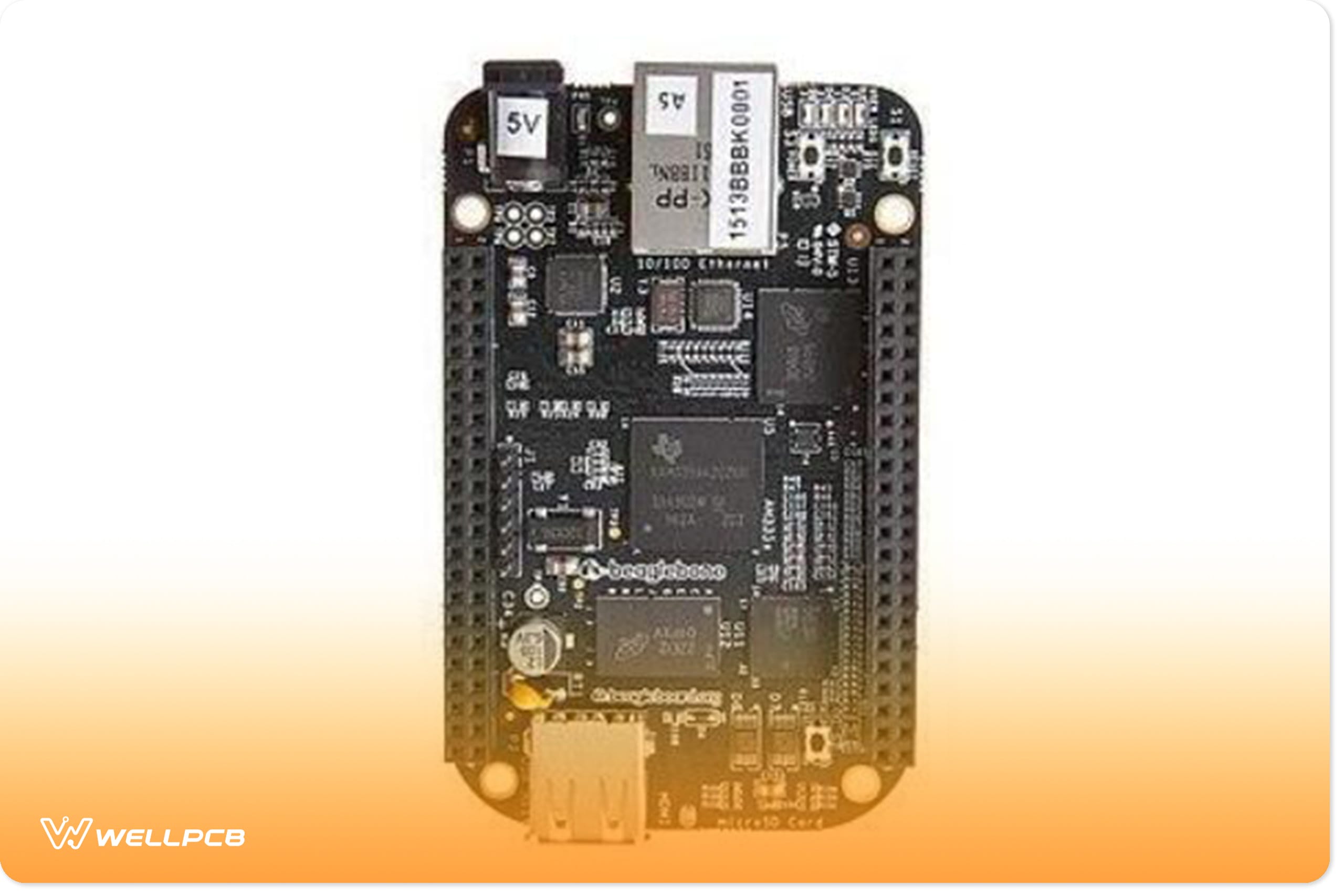
Beaglebone Black Pinout: Pin Configuration, Specification, and Application
Laptops changed the game in tech. Just like a laptop, Beaglebone Black pinout is far packed with a powerful processor, memory, and picture acceleratio...
SPDT Switch Wiring: Everything You Need To Know
Knowledge of electronic components and household technology can give you the power to troubleshoot things yourself. To better understand your home, tr...

Passive Tone Control Circuit: Applications, Design, and Benefits
Why do you need an audio tone control circuit? First, it allows you to regulate the signal’s bandwidth going into the audio power amplifier. No doubt,...
Air-Core Inductor Design: All You Need to Know
One of the smallest yet essential parts of an electrical component is an inductor. Inductors are electrical devices that store energy when current flo...

Voltmeter IC: A voltage measuring tool
About Voltmeter IC. Measuring the voltage between two points on your electronic circuit can provide numerous advantages. For instance, it lets y...

Trimpot Pinout: Complete Guide to Trimmer Potentiometer
As technology advances, the need for innovation arises. Previously, the trim pot pinout was non-existent. We only had the normal resistors.
However,...

LDO Circuit: The Basics, Working Principle, and Applications
Are you designing a power regulation strategy for your PCB? Or you're working on creating a custom power supply for your board? If yes, it's vital to ...
DHT22 Pinout: How it Works and its Application
If you have a faulty dehumidifier system, your home will have extensive mold growth, risking your family's health and property value. Besides, a dysfu...

DIY Ultrasonic Dog Repeller: Keeping Canines Away
Sometimes, you may come across an aggressive dog while walking in outdoor spaces, leading you to move as far away from it as possible. However, you ca...

MOSFET Protection: How to Properly Protect It
Nothing is immune to damage, and that includes MOSFETS. But why do MOSFETS get damaged? The bottom line is that MOSFETs experience damage when you use...
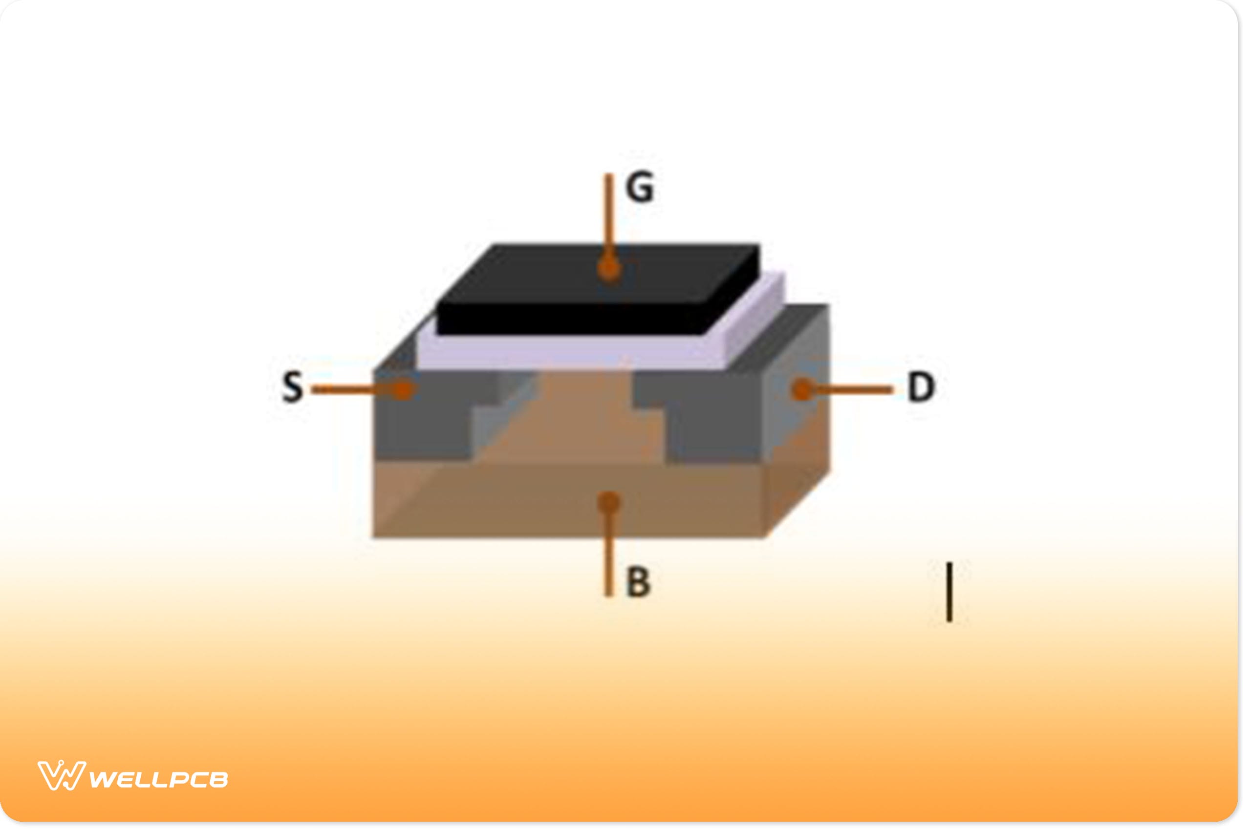
How Does a MOSFET Work: Basic Understanding, Types, and Applications
MOSFET stands for metal oxide semiconductor field-effect transistor. Like any conventional transistor, it is a type of transistor with many applicatio...

DIY Logic Probe: Step by Step Guide
A functional logic probe is one of the handiest tools you can have in your electronics workbench. This simple gadget shows you the logic signal levels...
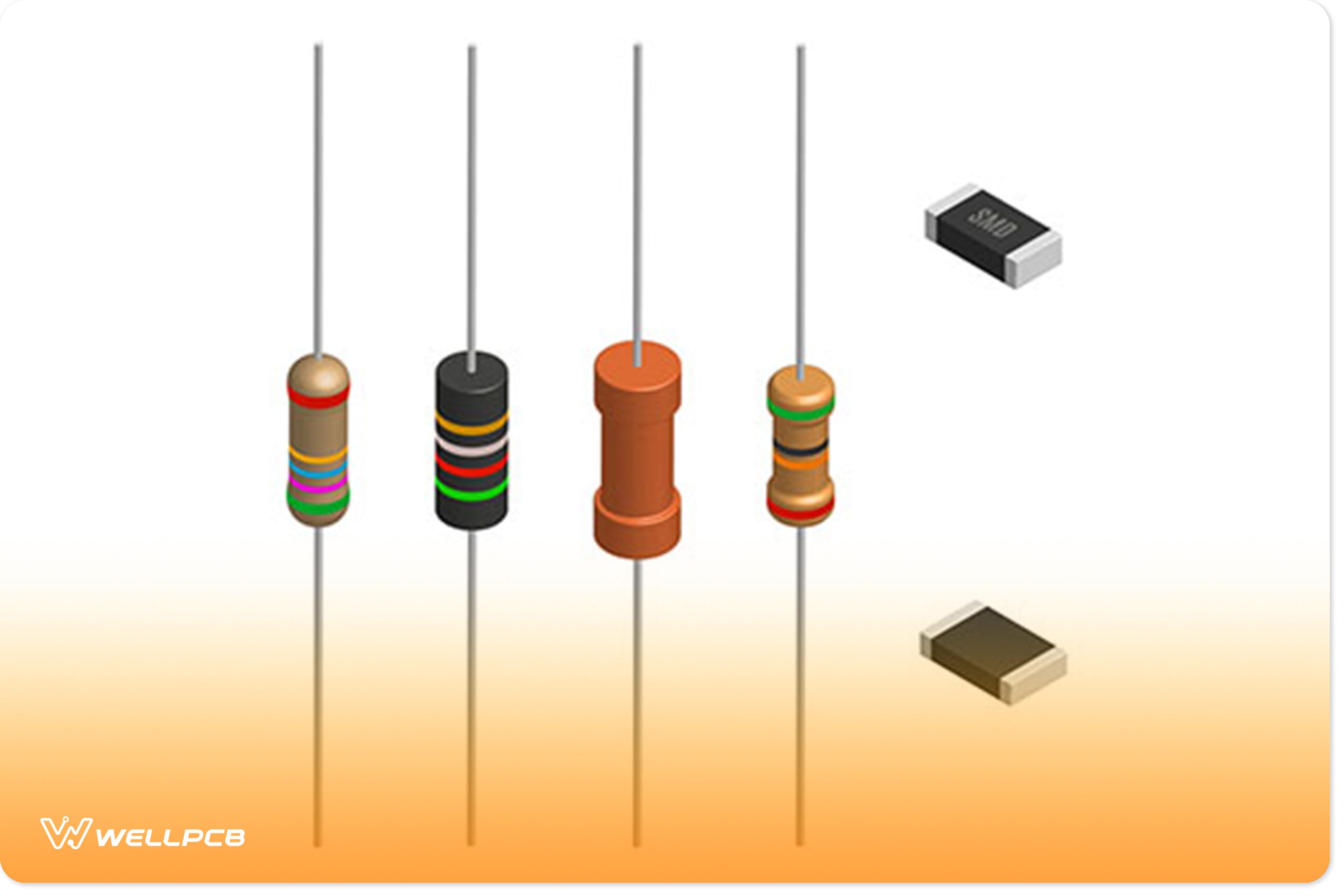
Resistor Circuit Diagrams: Understanding Connections and functions
Regarding Resistor Circuit Diagrams, Resistors are one of an electronic device's most critical electronic components.
They are passive components ...
Raspberry Pi Camera Pinout: What It Is and How to Use It
Closed-circuit television (CCTV) is popular these days. And it’s all thanks to its effectiveness in offering peace and security to users. But the syst...

High Current Voltage Regulator: The Definitive Guide
There’s hardly any electrical product that doesn’t require a type of voltage regulator. This fact makes the voltage regulator one of the most used ele...

Touch Lamp Circuit: A Comprehensive Guide
Several touch-sensitive electronic applications open doors to different and fun project ideas--for engineers and professional DIYers alike. One of suc...

Heart Rate Monitor Circuit: A Well-Detailed Guide
The heart rate monitor is a device you’ve most likely heard of before. Chances are you know one or two devices or persons that have heart rate sensors...

Automatic Voltage Regulator Project: Designing and Constructing Your Very Own Circuit
Most modern electronics require manipulated current and voltage to function correctly.
One could argue that Most modern electronics need to be man...

lm386 Amp: Everything You Need to Know
Amplifiers, which integrate into electronic circuits, improve sound quality, and these generally work by reducing noise distortion. One such amplifier...

Clapp Oscillator: Circuit Diagram, Frequency, Advantages, and its Applications
Oscillators are some of the most incredible gadgets used in modern-day electronic circuits. Consequently, we'll look at the Clapp oscillator, which is...
Transistor Saturated: What It Is and How to Identify One
Transistor Saturated? What does it mean? Well, this term can only make sense if you're a designer or engineer that's quite familiar with transistor sw...
Schmitt Trigger: Circuits, Working, and Applications
Schmitt Trigger, known initially as the thermionic trigger, has been around for decades. So far, it has contributed to life-changing technological adv...

Clap Switch: An Easy Project for Beginners
Are you a beginner looking for a simple project to test your skills, or are you a seasoned hobbyist looking for a fun project to build? Well, you've c...

Ultrasonic Sensor Circuit: A Complete Guide
Animals such as dolphins and bats use acoustic noise and sound to navigate and expose their surroundings. This phenomenon is called echolocation. Desp...

Isd1820: A Voice Recorder Module Guide
Have you ever wanted to create a voice recording but didn't know where to start? The ISD1820 recording module can lead you in the right direction! Tha...

Audio Circuit Mixer: 5 Ways of Building an Audio Mixer
An audio mixer/ mixing console is a device that combines, then modifies audio signals. Afterward, there's a summation of the modified audio signals to...
Ferrite Core Transformer: A Definitive Guide on the Basics
Most electric power transformers have secondary and primary windings as the basic features. Other times, there can be tertiary windings. As such, ther...

Audio Delay Circuit: Creating Echo and Reverberation Effect in Audio
Sometimes, the audio output we get is not good enough. It's either not rich or comes off bland and makes our ears tingle. To avoid this, we introduce ...

VFD Schematic: VFD Circuit Diagrams, Types, and How to Build One
Every electronic enthusiast has come across the term VFD.
VFD stands for Variable Frequency Drive, also known as Variable Speed Drive or Inverter. I...
FET Test: How It Works and When It’s Needed
FETs are pretty crucial in circuitry. But it's easy to install a defective FET in your circuit, which will lead to some undesirable results. Luckily, ...
Potentiometer Circuit: How They Work and What They Are Used For
Potentiometers are electronic components. This article will describe this resistor in detail. And so, keep reading to learn more....
USB Port Pinout Guide: Pin Configuration & Connector Layout
The Universal Serial Bus (USB) is integral to modern digital devices. It provides electronics and computer makers with a unified way (standard) to tra...

Arduino Joystick Module: How to Effectively Make One
Are you currently handling projects related to motion and robotics? Then, there’s a chance that you’ve probably heard about the Arduino Joystick modul...
DIY RFID Reader: How to Make One That Works Effectively
Does your project involve radio wave frequencies, and you’re looking for a great project idea, or have you heard about DIY RFID Reader before and want...

Replace Transistor – How to Make the Best Choice
When repairing electronic systems or electronic devices, finding an exact replacement is difficult. In most cases, you will have to use substitutes. N...

Alarm Circuit Diagram & DIY Projects | Schematics
Without a doubt, an alarm circuit is one of the best DIY projects you can undertake. Alarms have become an integral part of modern homes, alerting us ...

Tachometer Circuit: How it Works and How to Make One
It's not enough to build high-powered electronic circuit boards or machines that use engines.
Why?
Because such projects won't be complete if ...
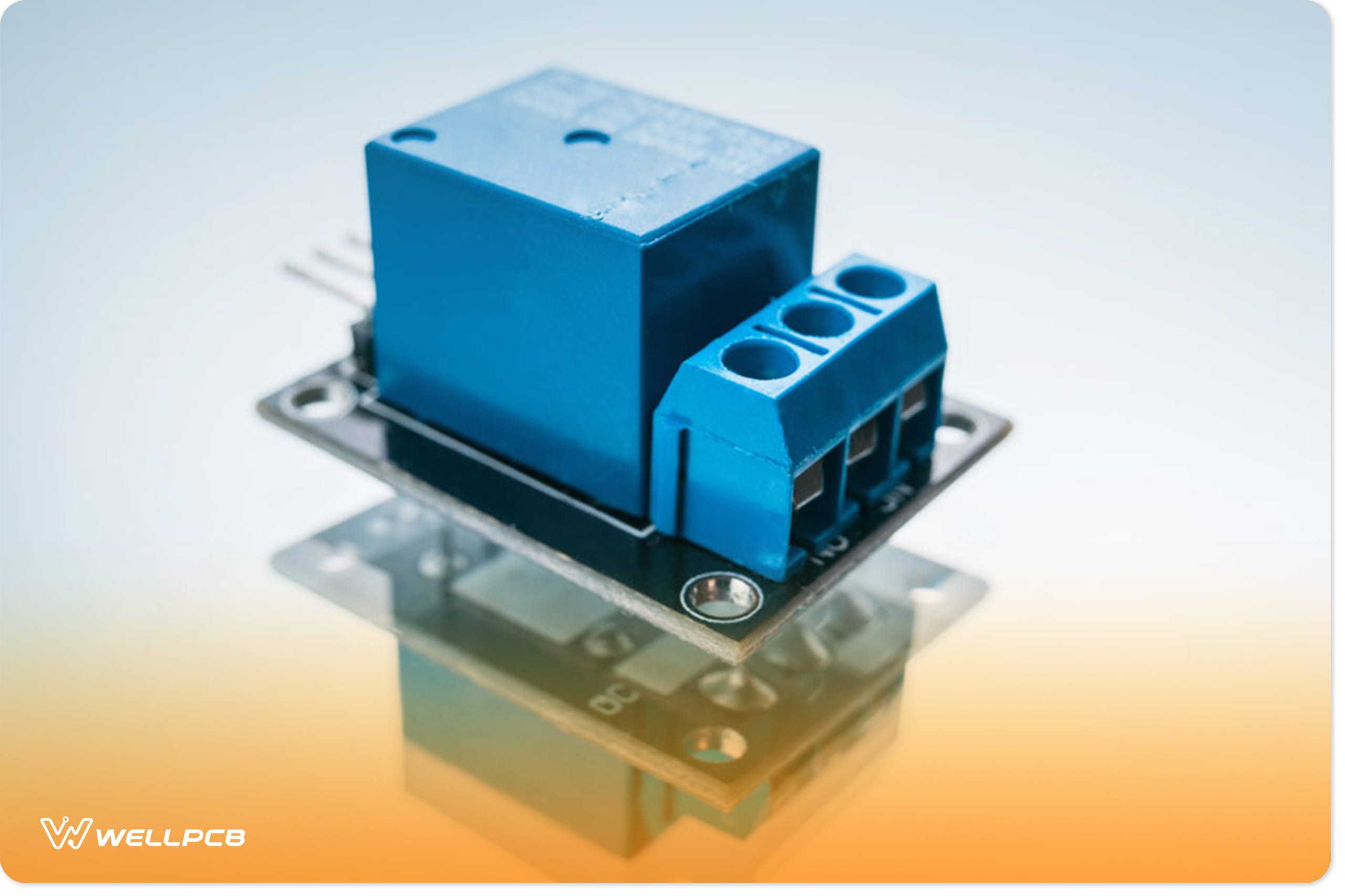
8 Channel Relay: Everything You Need to Know
Have you ever wanted to control multiple loads at once but weren’t sure where to begin? An eight-channel relay module can now provide that solution! T...

Types of Inductors: The Ultimate Guide
Inductors have a reputation for being large and sluggish. Thus, some hobbyists may avoid them - especially when starting. However, they're a critical...
Bd139 Pinout: The Only Comprehensive Technical Guide You’ll Ever Need
When you want to control high currents or voltages, chances are the first thing that comes to mind are Darlington transistors. But if you don't have a...
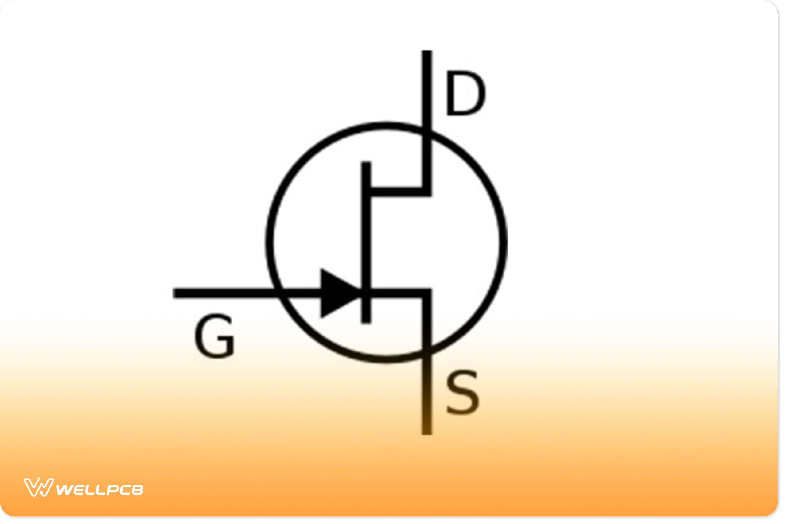
2N3819: The Ultimate Guide
Many JFET types exist today. Each of them provides special features/specifications that present various circuit applications. Now, in this article, we...
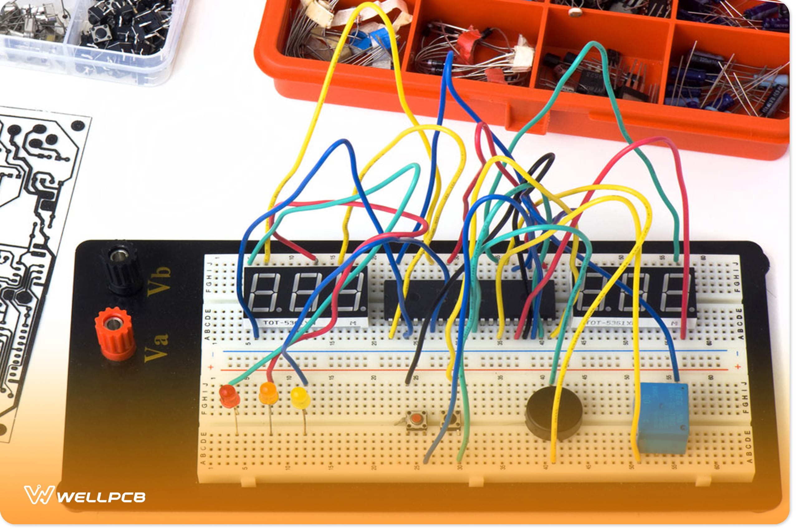
Variable Voltage and Current Power Supply Circuit- High-quality Variable Stable Output
An ideal power supply unit must feature a variable voltage and current power supply circuit. The property is most important in common laboratory uses ...
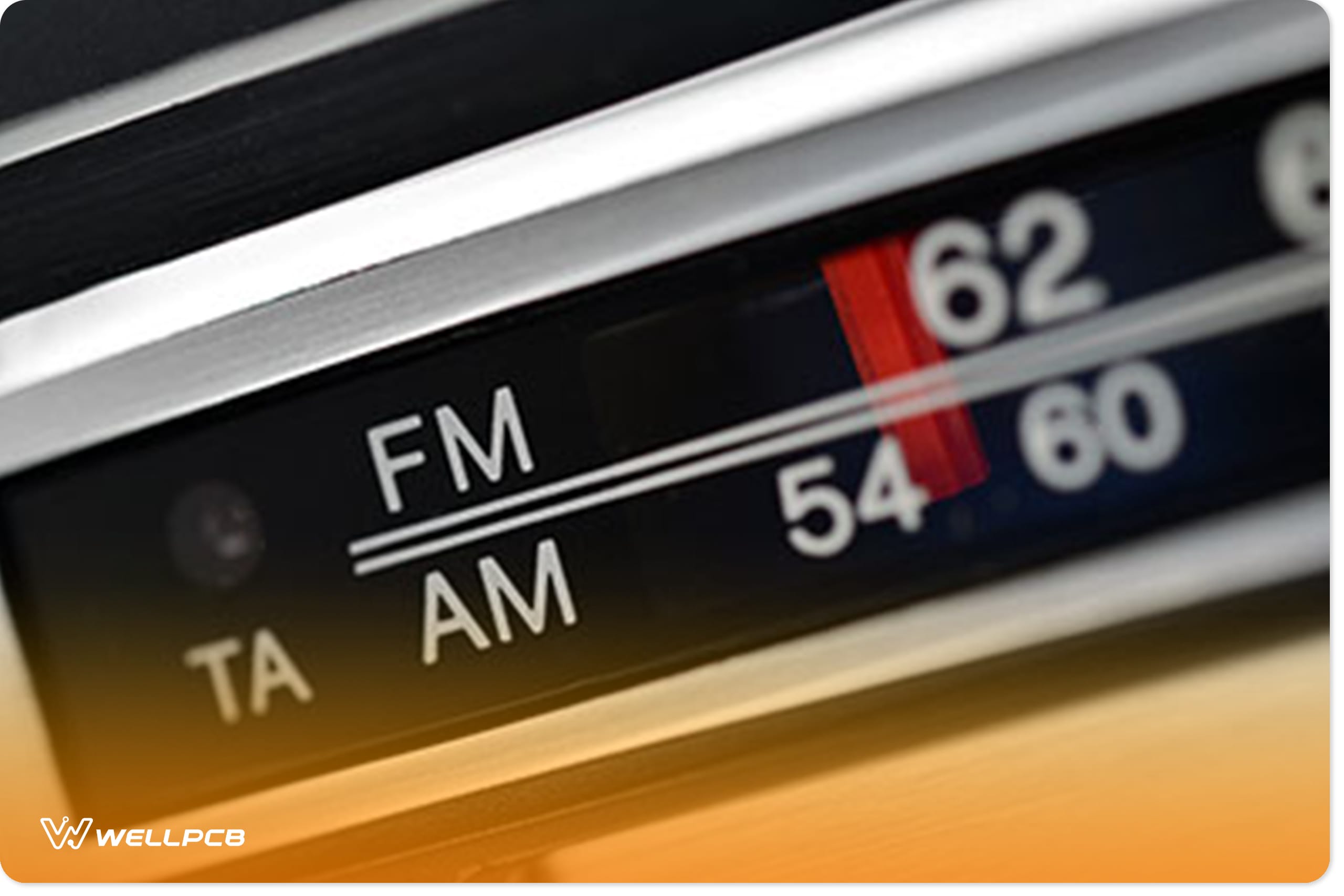
AM Loop Antenna: Everything You Need to Know About It
Building an AM broadcast radio receiver can be a fun project. But, certain limitations can hinder your radio experience—like weak AM signals. AM recep...
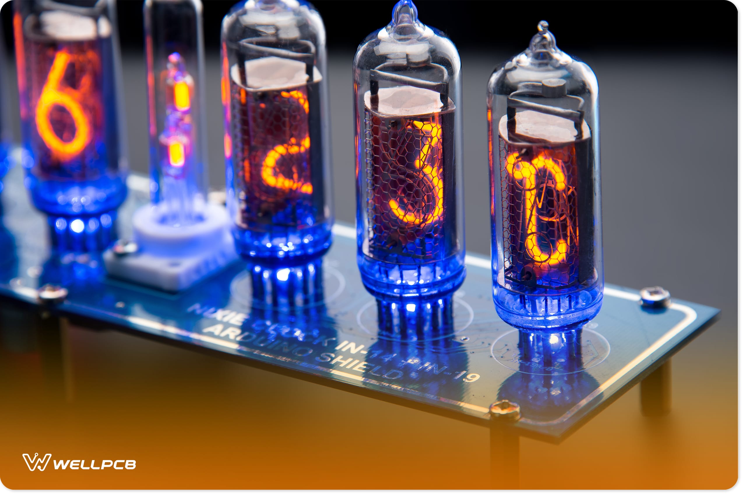
Neon Lamp Circuit: What Is It and How It Works?
Various electronic circuits come with visual indicators and sometimes even appliances. Also, these visual indicators are important because they help s...

Opamps Hysteresis: The Ultimate Guide
Many fundamental concepts in the technical world are hard to deal with because of how deceptive their meanings can be. Unfortunately, Hysteresis is on...
IC 4060: Understanding the Pinout and their Functions
Generally, an IC 4060/CD4060 timer chip is a Timer IC or oscillator in some instances. It belongs to an IC 4000 series of Integrated Circuits and oper...
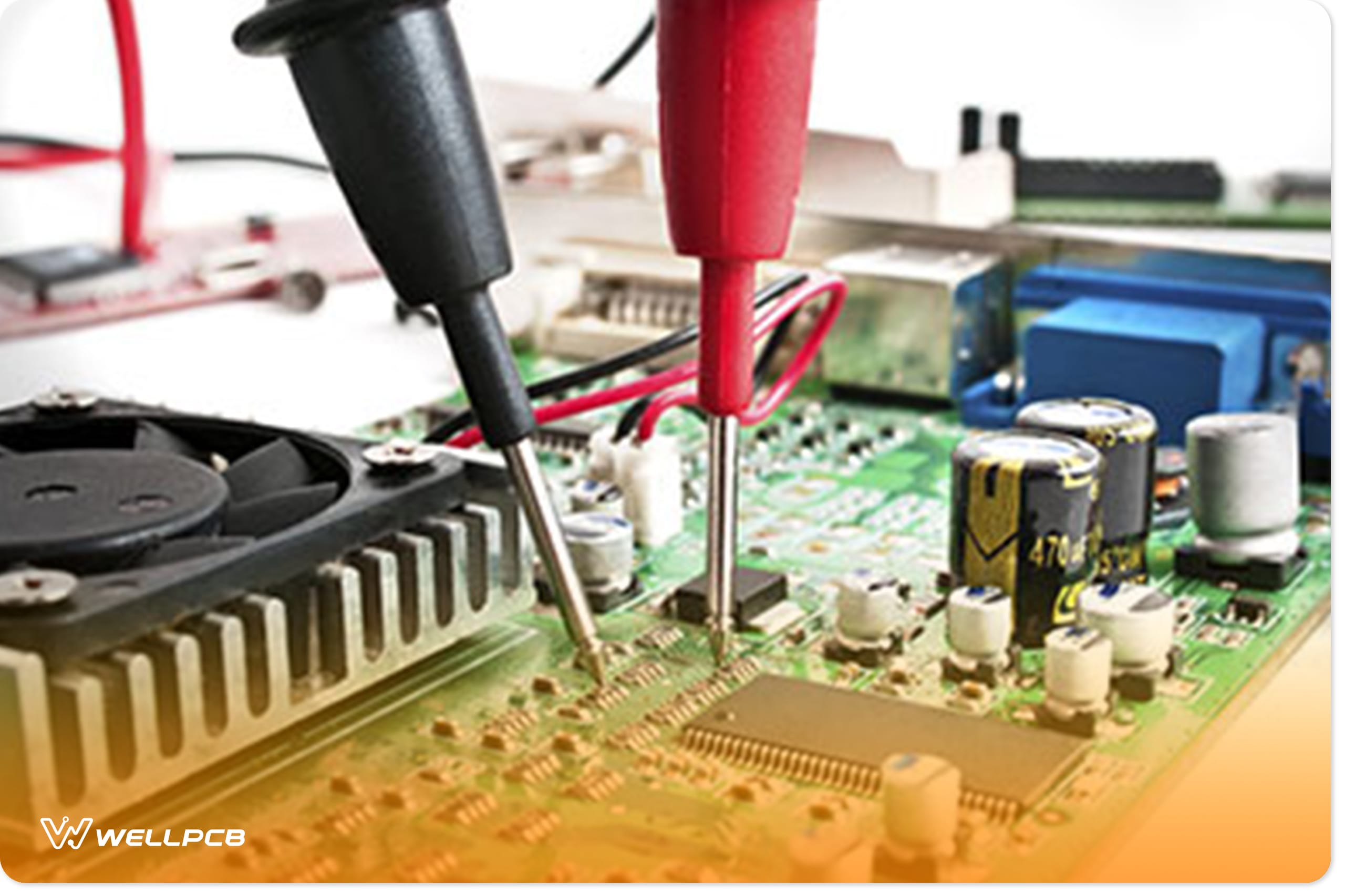
Continuity Tester Circuit: How to Build a Simple Continuity Tester
All electrical outlets get faulty from time to time. When an electrical device develops a fault, such defects often arise due to a disruption in one o...

How to Make a 12 volt Battery: A Short and Clear Guide
A 12-volt battery is a rechargeable battery that has grown in popularity because of its many different uses. As an electronics enthusiast, your need t...
How to Make an Arduino Proximity Sensor: Hardware Components and More!
An Arduino proximity sensor is a handy, inexpensive gadget that detects the presence of an object within its sensing range. This could be anything fro...

Voice Changer Circuit: Building a Voice Modulator Circuit
About Voice Changer Circuit, Voice modulation is a captivating and fun project that we've had to work on so far.
Often, its circuitry involves transf...
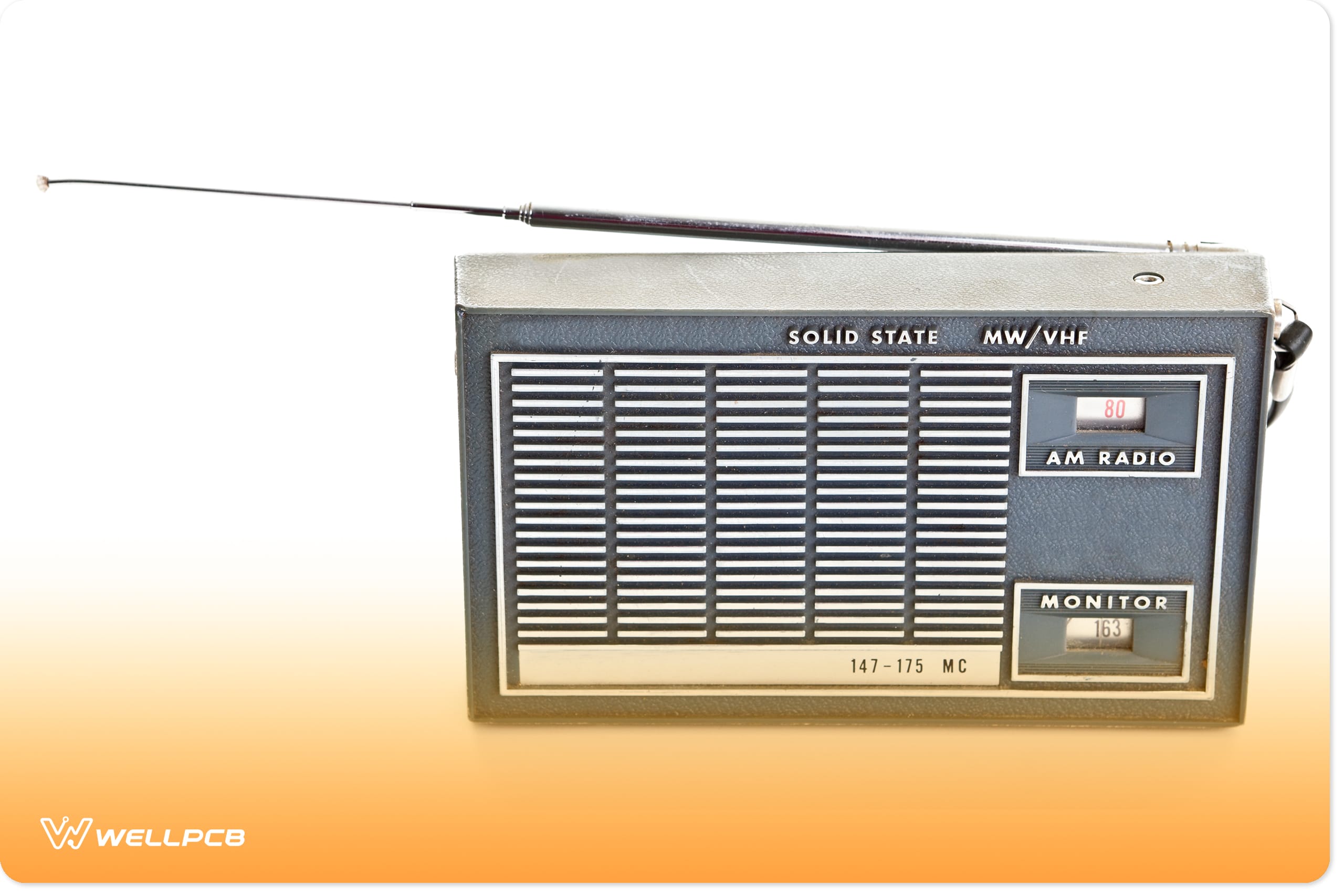
AM Radio Schematic: A Guideline on Making Simple Circuit Diagrams
Want to know something about AM Radio Schematic? An AM radio receiver circuit can use either one or more transistors alongside other electric componen...
Transformerless Inverter -All You Need to Know
Sometimes, technology can make giant leaps forward for the collective community. Transformerless technology is one of these developments. It offers ut...

Ripple Carry Adder: Everything You Need to Know
Logic circuits may rely on a ripple carry adder to add n-bit values together. As a result, this digital circuit implementation provides useful feature...

Piezoelectric Effect: How It Works & Complete Guide
Most modern devices use piezoelectricity as a component of their Printed circuit boards (PCBs). For example, your quartz watch needs piezoelectricity ...
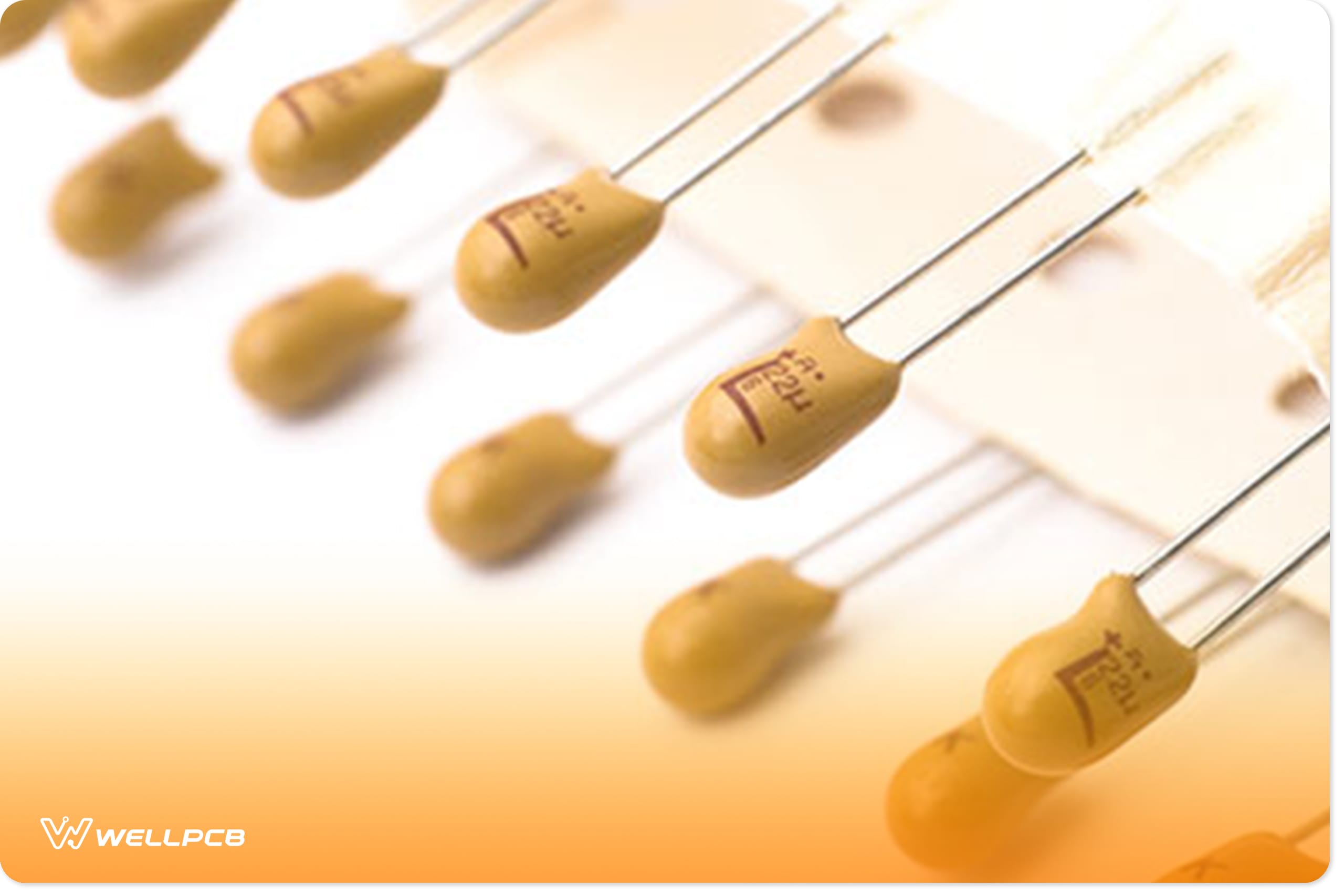
Tantalum Capacitor Polarity Markings – Complete Guide
Do you know the Tantalum capacitor marking? Tantalum capacitors are electrolytic capacitors and reliable components of PCBs. These capacitors are of d...

Refrigerator Alarm: What Is It and How It Works?
Have you ever discovered your fridge door was slightly open all along and most of your food has gone wrong? Or, does your fridge door need that extra ...
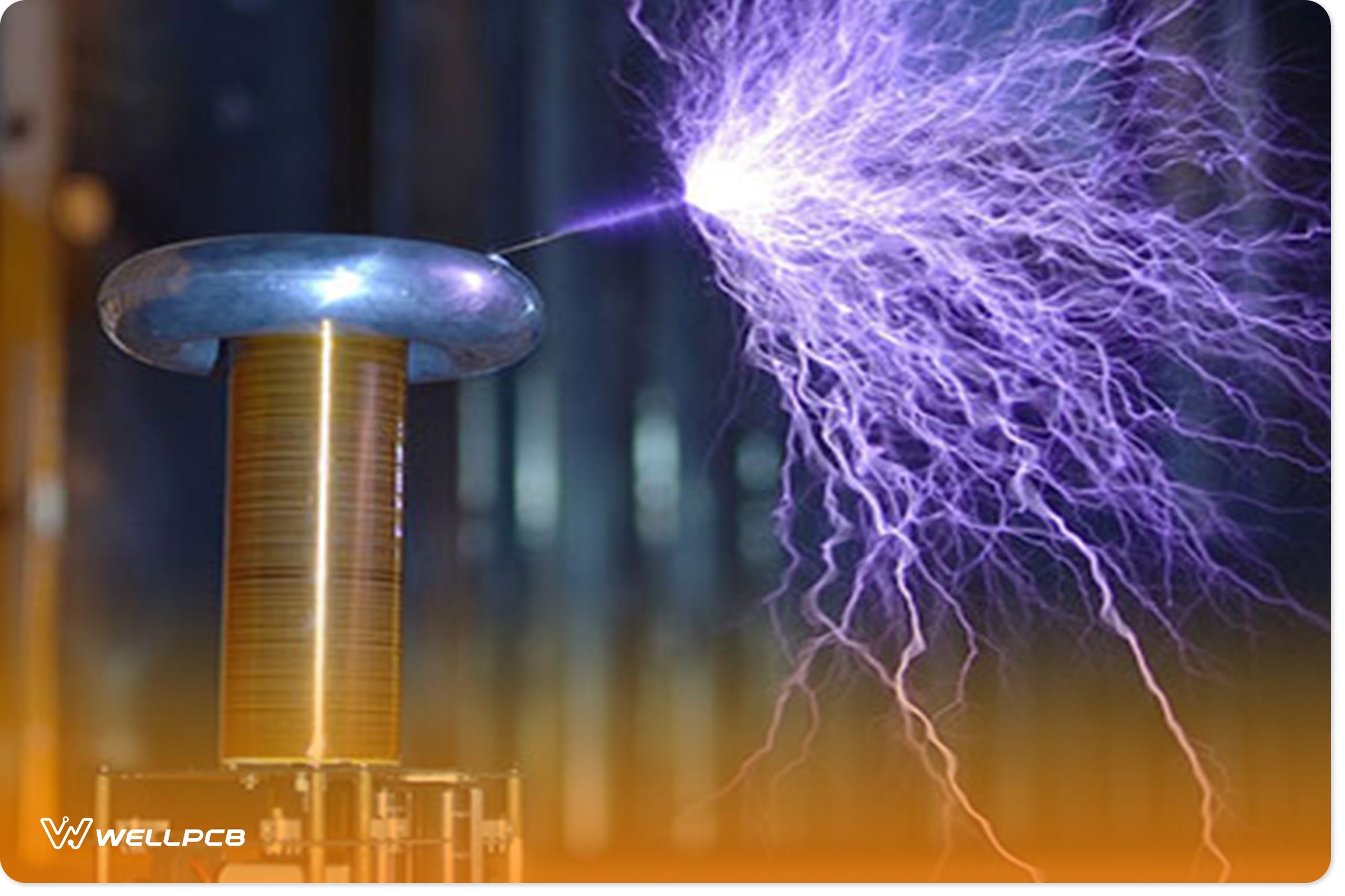
Circuits With Free Energy: Is it Possible to Make Free Energy?
Can we get energy for free? How can we get the power, and is there a way to store the electricity we collect?
Below, we will look at a device that...
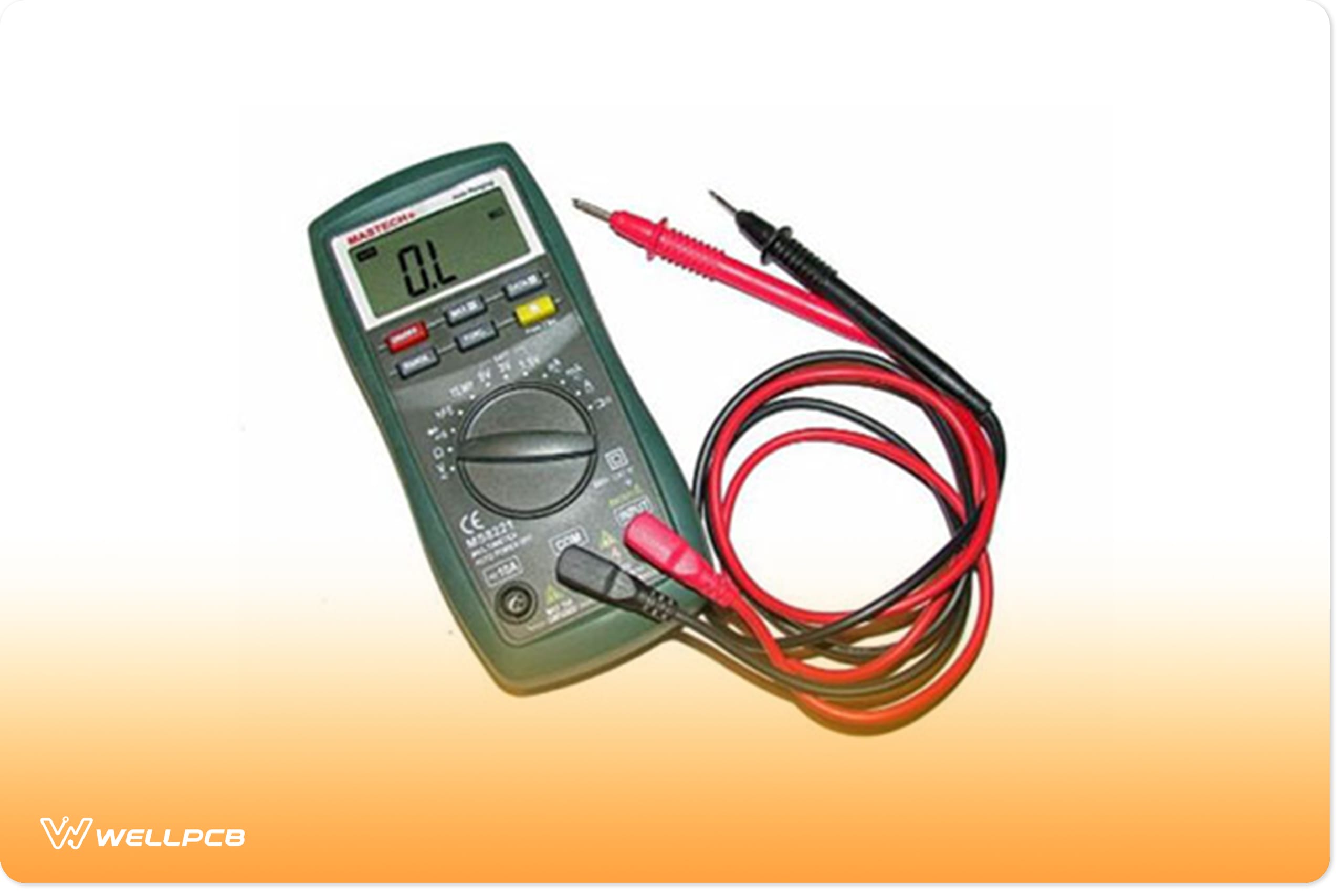
DIY ESR Meter: Everything You Should Know About a DIY ESR Meter
This article is about bout DIY ESR Meter. Every trade has its unique set of tools. In the case of electronics, you should at least have a multimeter, ...

Transistor Latch: A Comprehensive Guide That Explains Everything
Ever wondered how alarm clocks work? Or how buzzers or LEDs can stay on for so long without turning off? Well, until the power resets or someone flips...
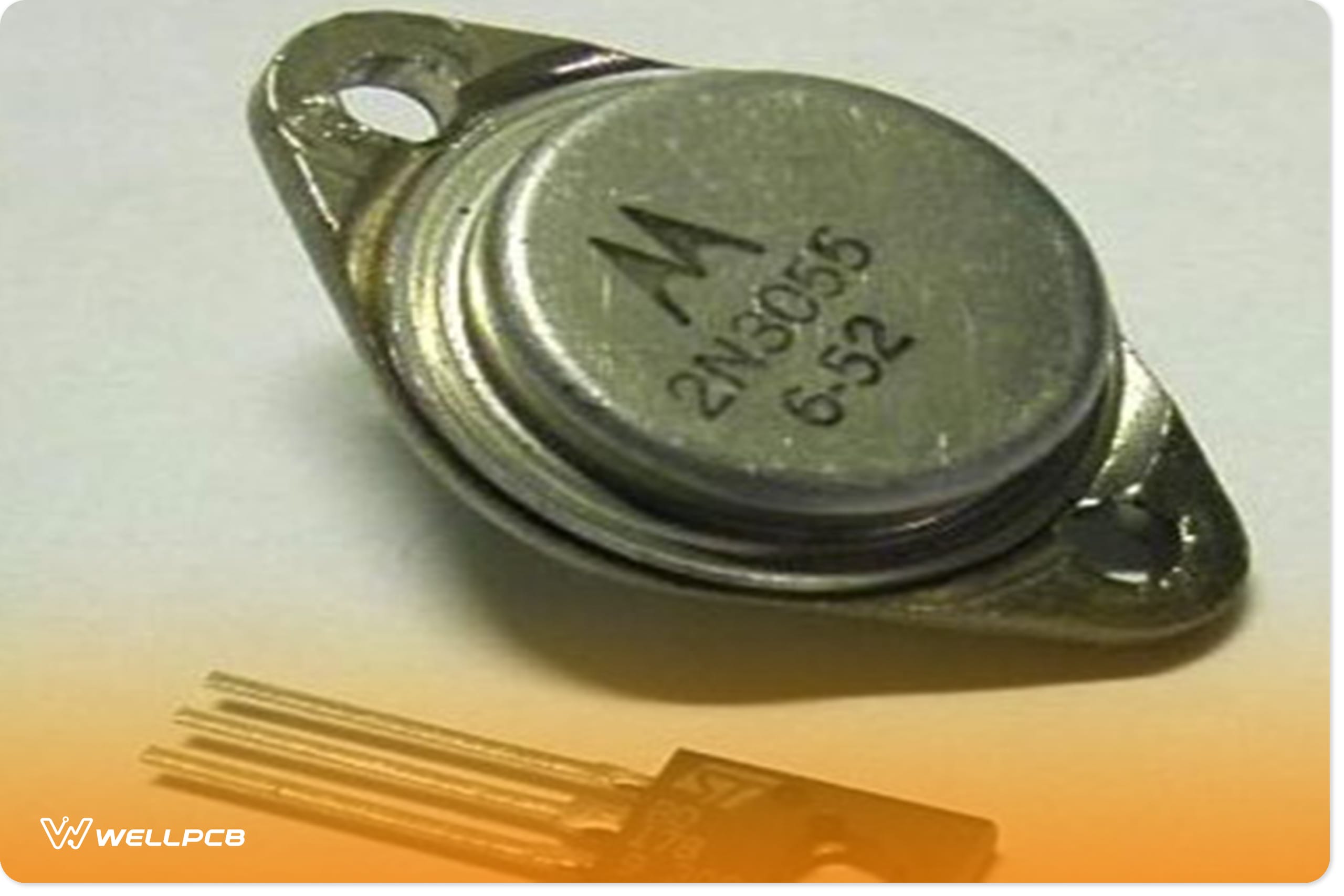
BJT Load line: A Better Understanding of The Function
A BJT load line, or a Bipolar Junction Transistor, provides for both electrons and electron holes as charge carriers. It allowed a small current to be...

Noise Filter Circuit: Improving the Sound on your Listening Device
You may notice that the sound from your music player or listening device seems distorted or unclear. That’s usually due to a poor amplification proces...

RTOS vs GPOS: A Complete Guide
In this modern era, we’ve seen a lot of software and hardware solutions that require an operating system. Operating systems help these devices run smo...

Hypersonic Sound System: The Complete Guide for HSS
Ever wonder how light reflects back and forth between the semi-reflector and reflector in lasers? Well, what if it told you it’s easy to make somethin...
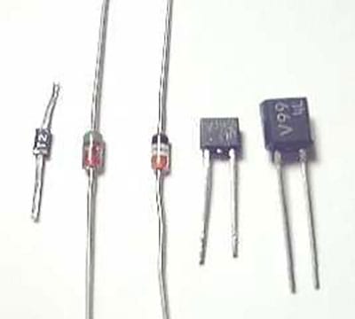
Varicap Diode: The Ultimate Guide for Electronics Enthusiasts
Electronic circuits typically consist of resistors, capacitors, transformers, diodes, transistors, etc. Now, we will introduce a special diode type. V...
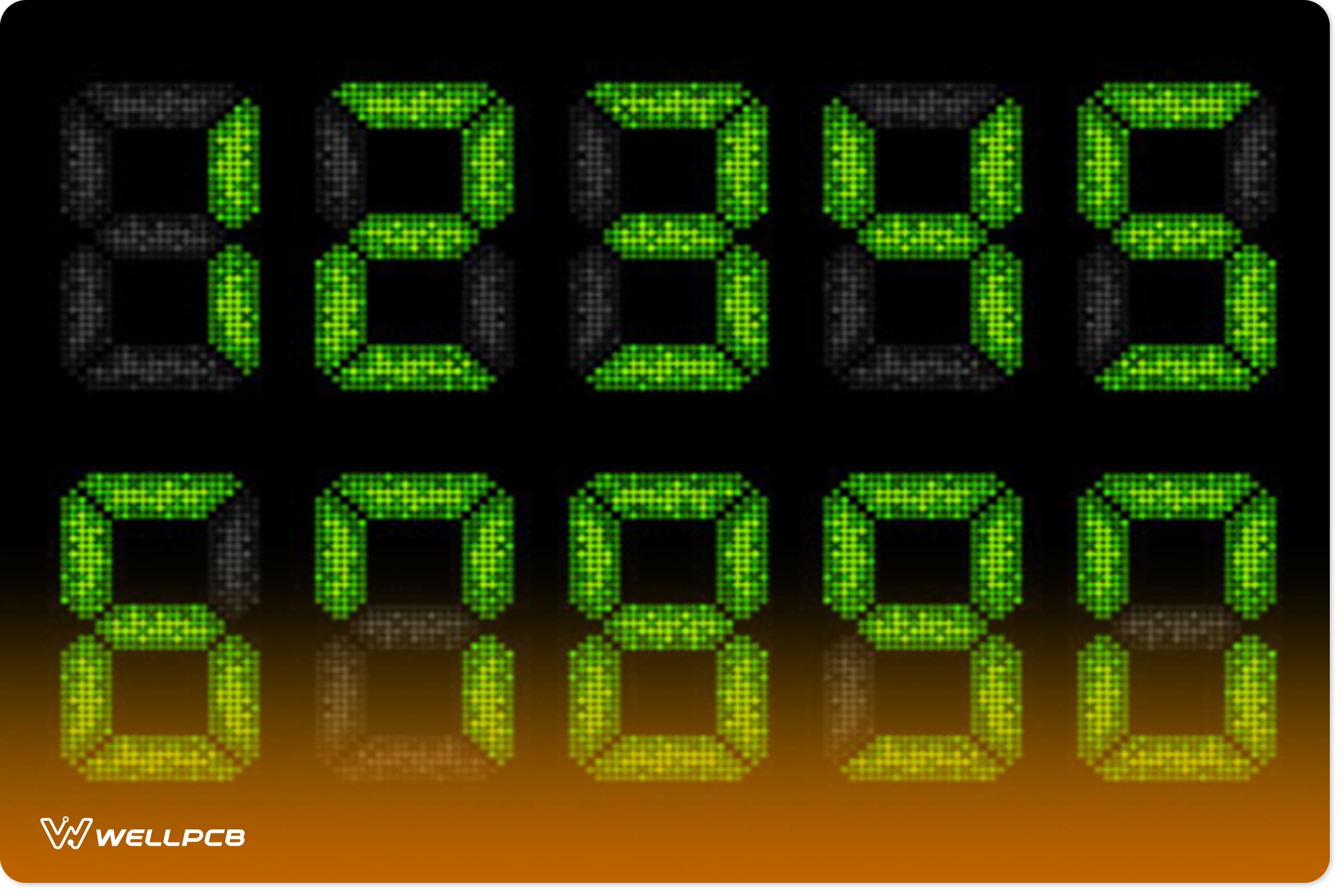
74LS47: Understanding The 74LS47 Data In Details
Two active-low outputs on the 74LS47 IC may drive common-anode LEDs or incandescent indications. As an input, it takes a binary-coded decimal, thereby...
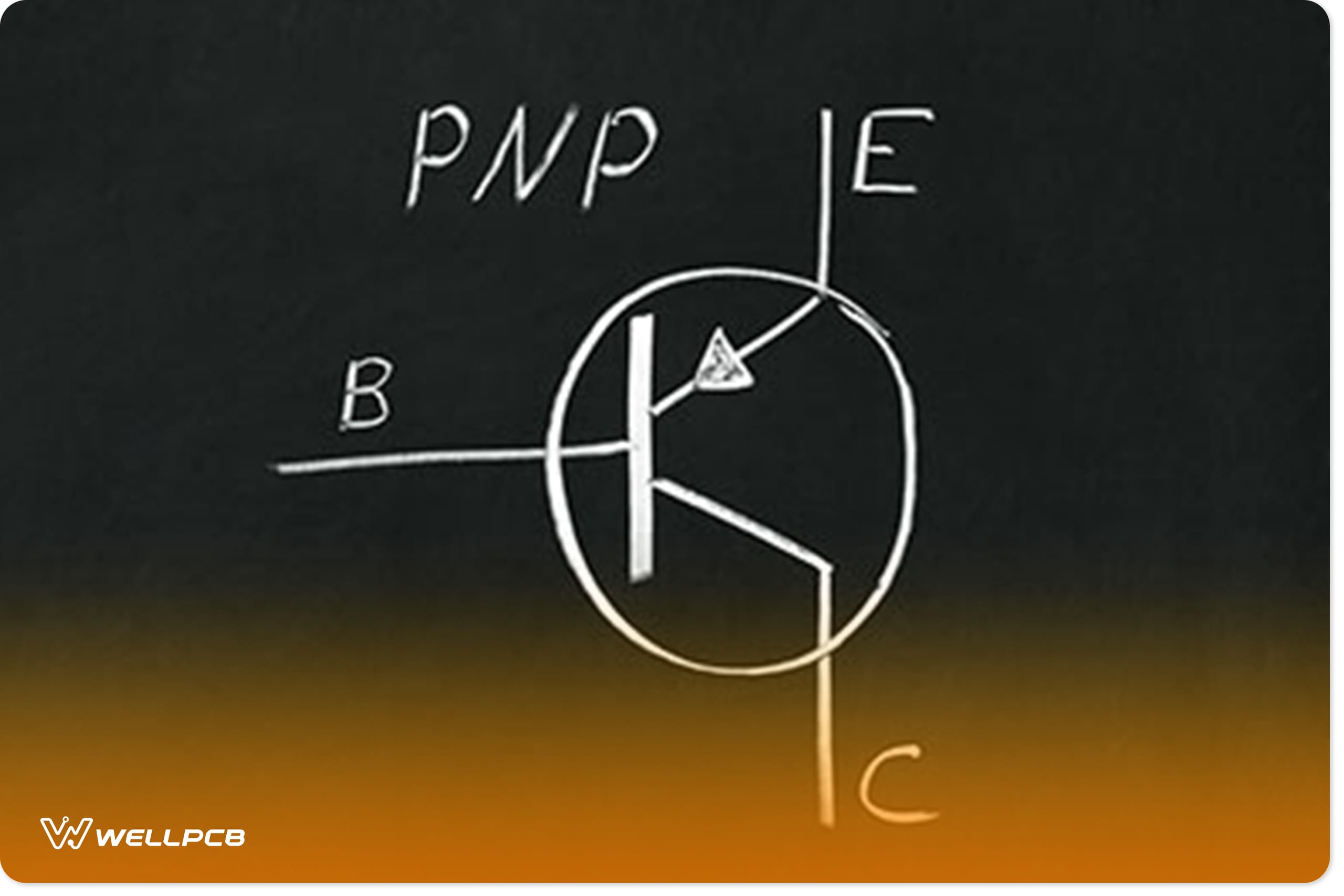
Tip120: Basics on TIP120 Transistor
NPN and PNP transistors commonly form part of the Bipolar Junction Transistor. Generally, electronic devices contain transistors whose function is not...
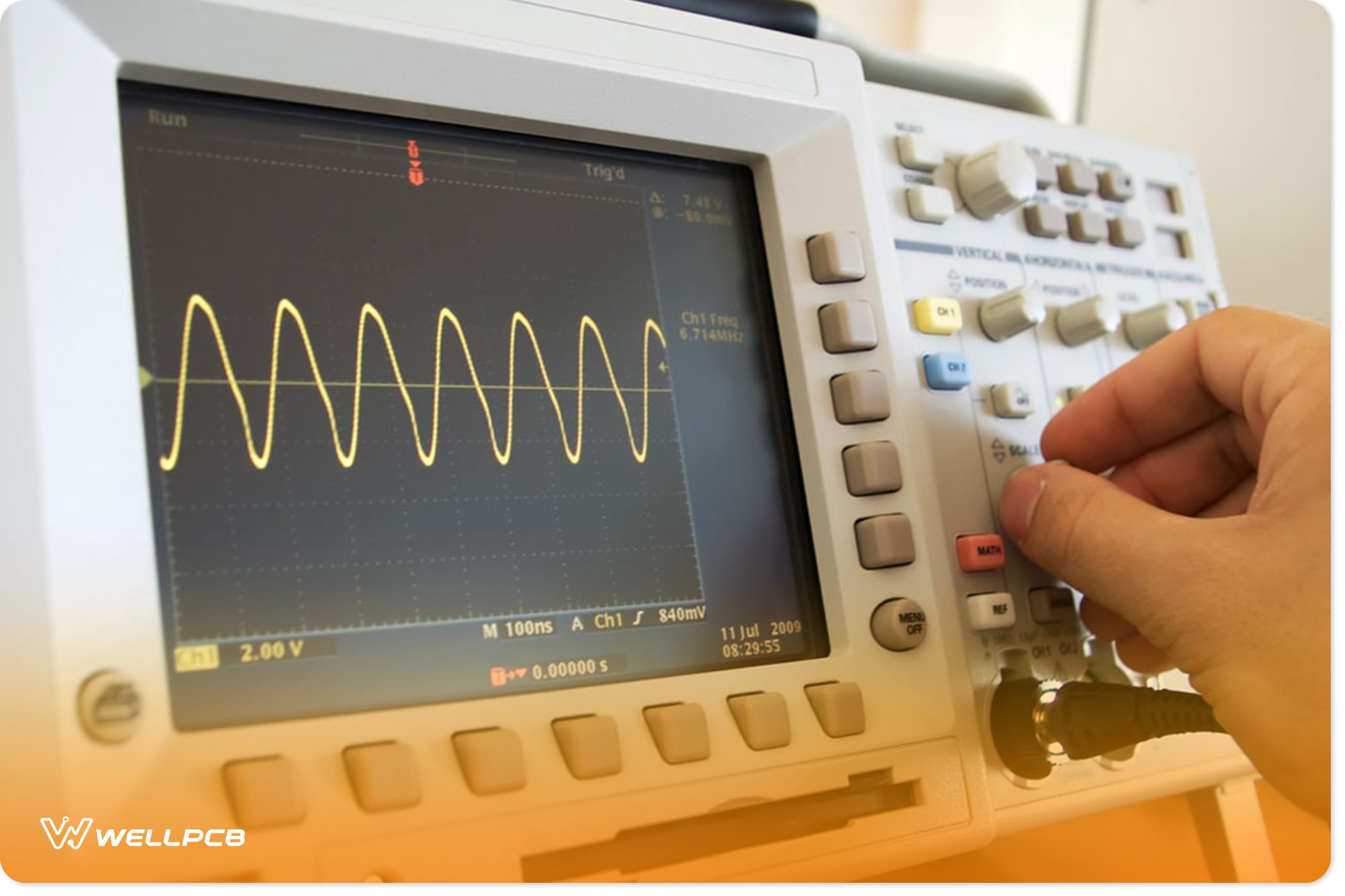
Analog vs. Digital Oscilloscope: What’s The Difference?
Oscilloscopes are important testing tools in electronics engineering. Especially when we measure a section of a repetitive waveform or a high-frequenc...

555 Oneshot Circuit: Understanding Monostable Designs
One can say that the 555 Timer is one of the most common chips used in DIY electronics today.
Once you better understand how they work, they are sma...
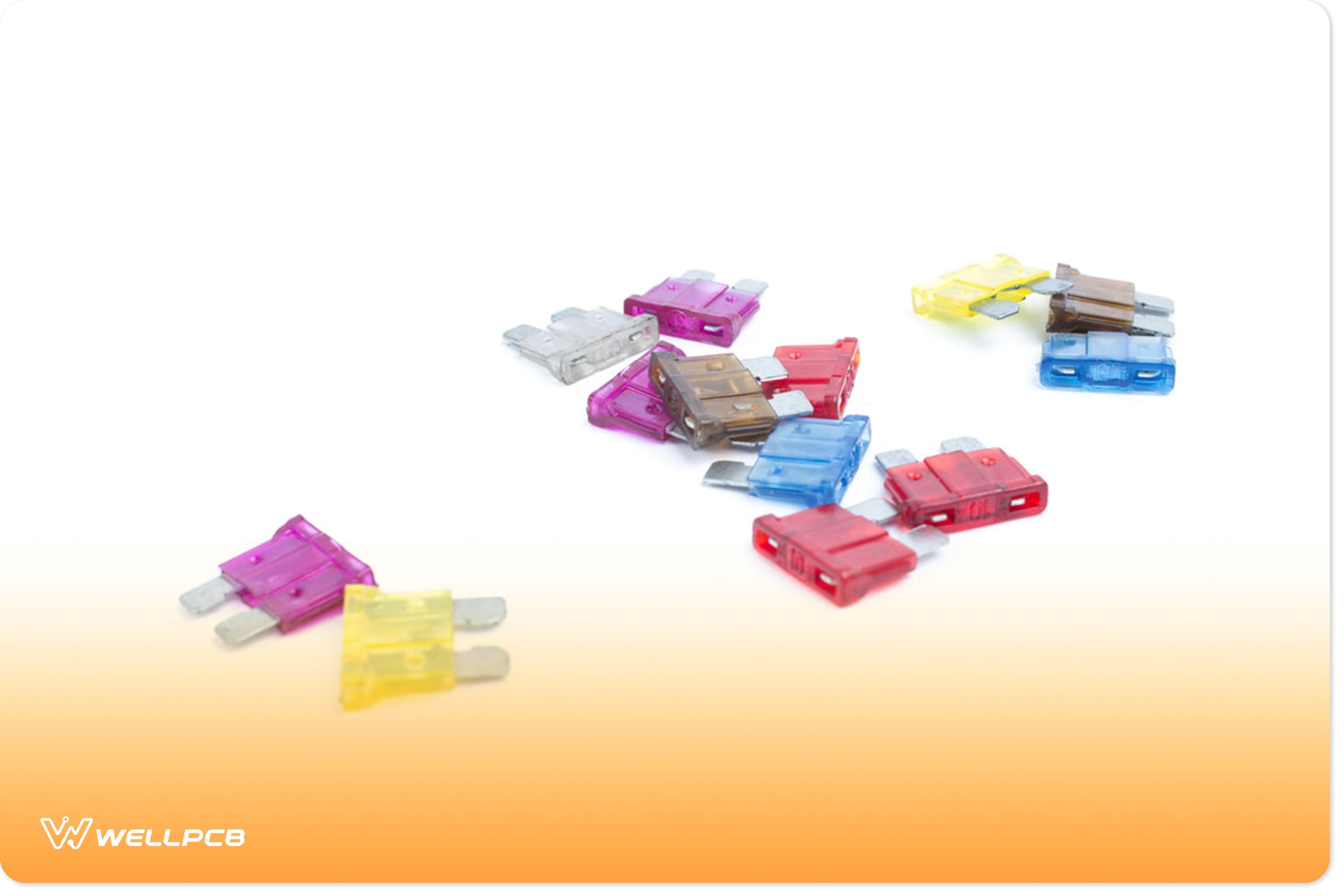
Types of Fuses: The Ultimate Guide for Fuses
Every electronic application needs a circuit. But, circuits are fragile and will get damaged when there’s a flow of excessive current or electrical fa...

DIY Digital Analog Converter: The Complete Guide
Translating digitally stored information from an iPod, laptop, or other audio equipment into the analog sound we hear can be a tricky project.
As eas...
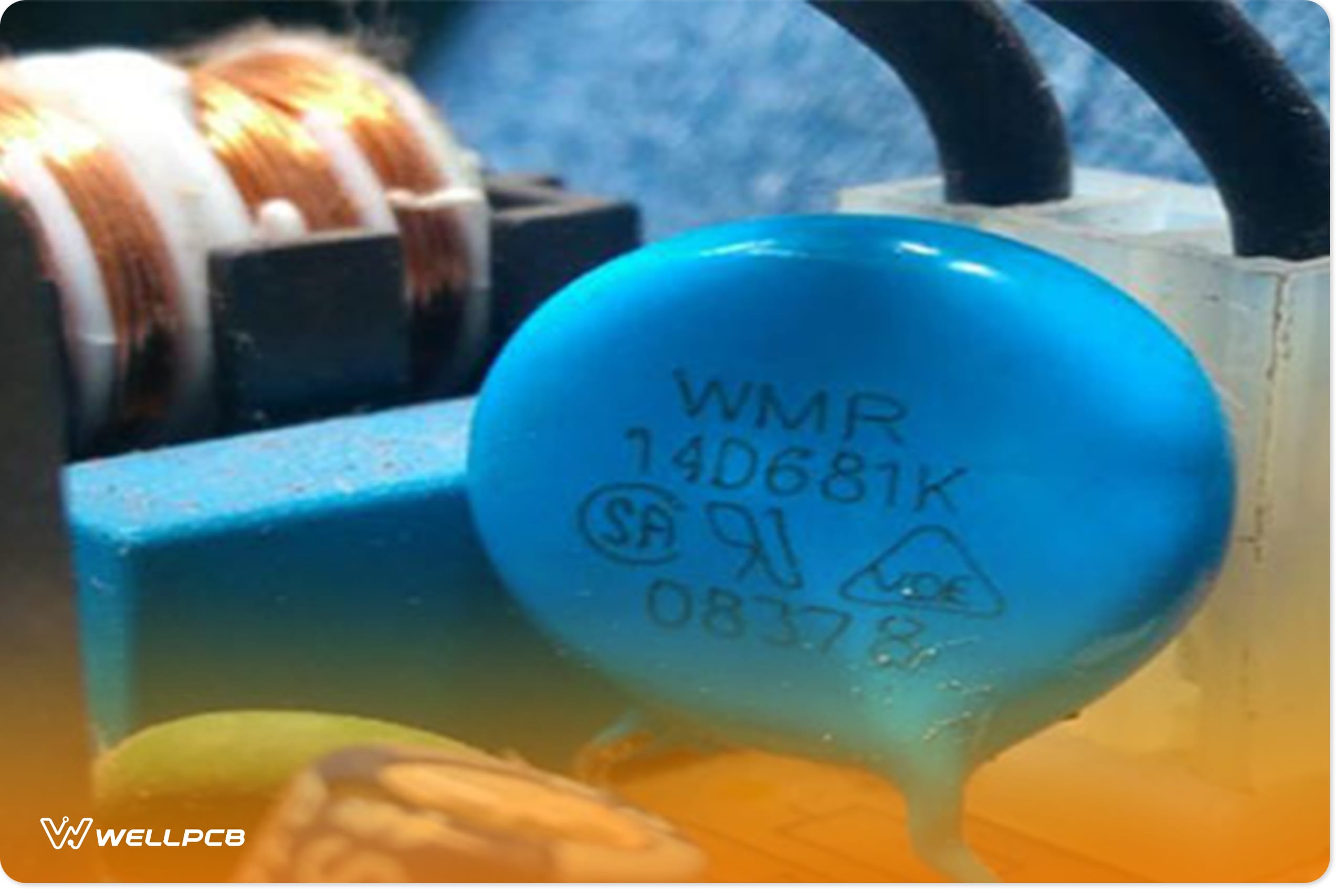
What Is a MOV: Metal Oxide Varistor Tutorial
What Is a MOV? Not every project requires a considerable voltage supply. Sometimes, you need to supply your circuits with a specific amount of voltage...
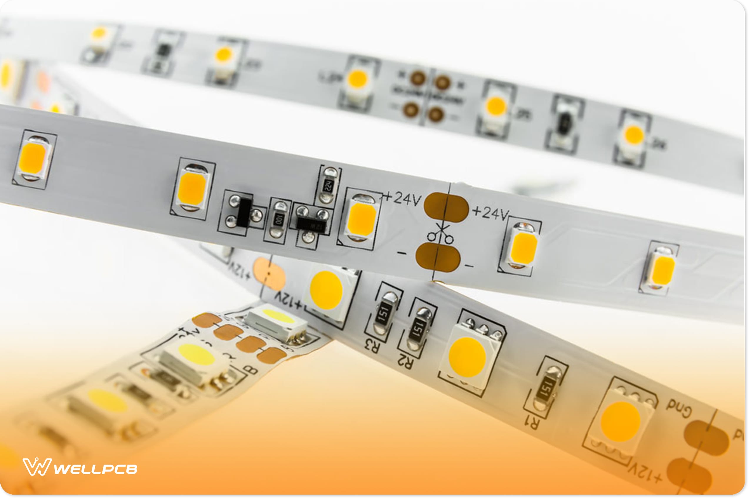
Transformerless Power Supply: The General Basics, Working, and Requirements Explained
Generally, electronic products have a step-down transformer that enables the DC power supply to convert AC mains voltages to a DC voltage (often small...
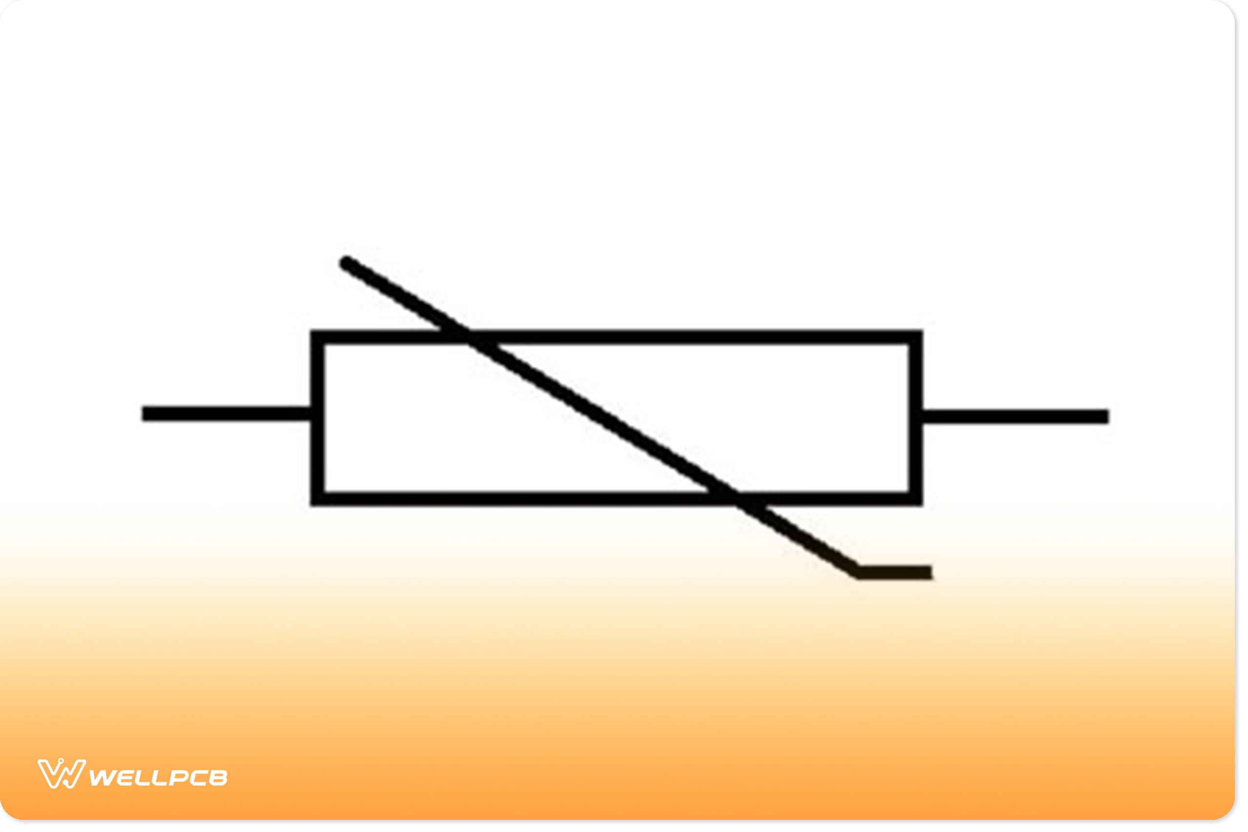
Varistor Symbols: A Complete Guide On Its Working and Applications
Picture this: you’re working on your electrical project smoothly. Then, you start having issues with high-voltage surges. First off, you’ll panic. And...
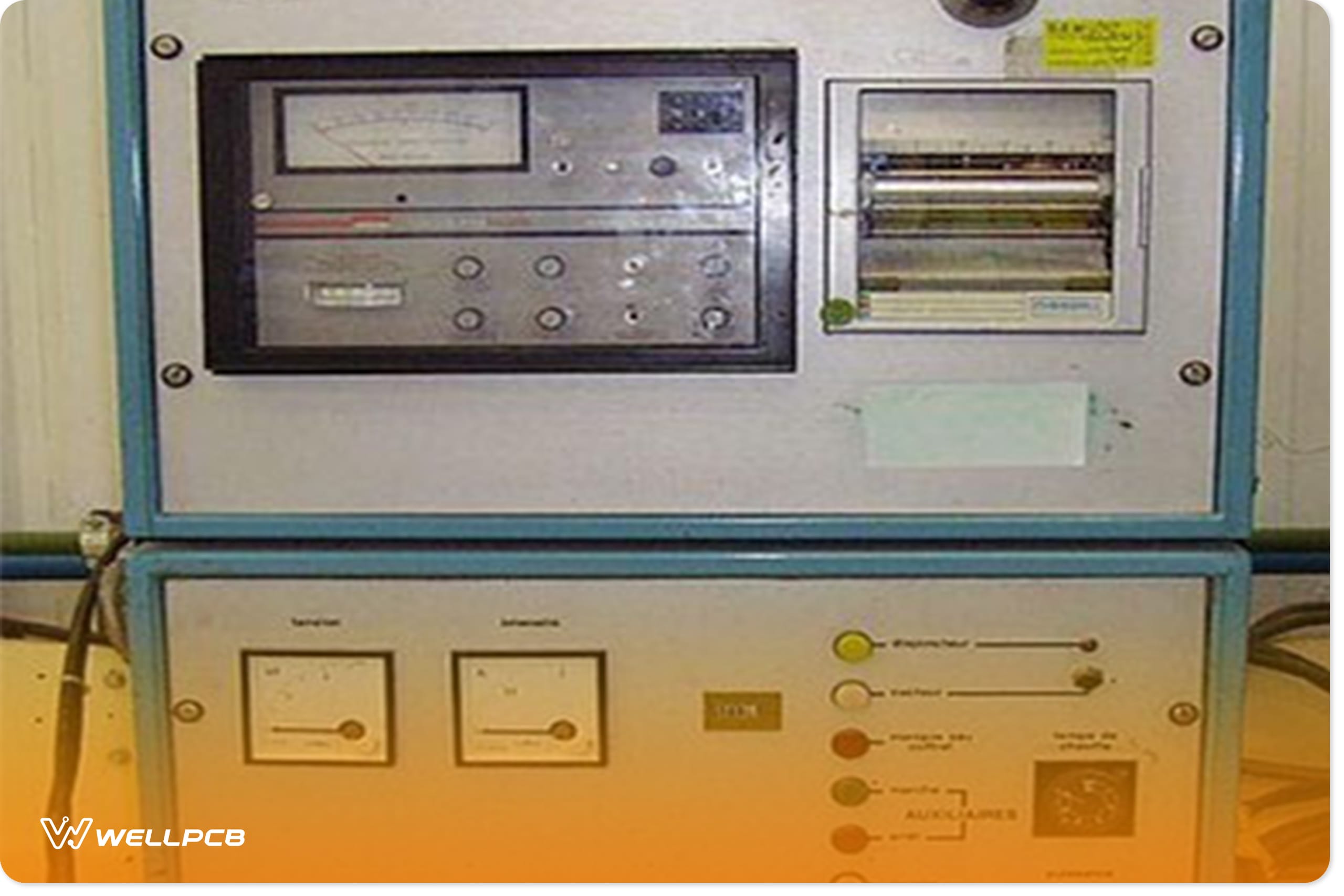
Induction Heater Circuit: Working Principle, Design and Applications of the Work Coil
People use the induction heater circuit for heating conductive materials in a non-contact process. It’s also a device that uses a high-frequency magne...

UPS Circuit: Everything You Need To Know and More
According to Statista, in 2019, ten countries were tied for first place for the highest quality of electricity supply.
However, it's always good t...

What is SCR: Everything You Need to Know
We all heard of a thyristor before, but what about the most popular type? An SCR, which stands for silicon control rectifier, acts as a switch while p...

How to Make a Rectifier: A Detailed Guide
A lot of devices use rectifiers to alter and improve power systems like wind turbines. So, if you’re looking to learn how to make a rectifier, how it ...

DIY Walkie Talkie: A Complete Step-by-Step Guide
A walkie-talkie is a simple, easy-to-use, and robust device that’s excellent for outdoor use.
The device is even more helpful when you have unavaila...
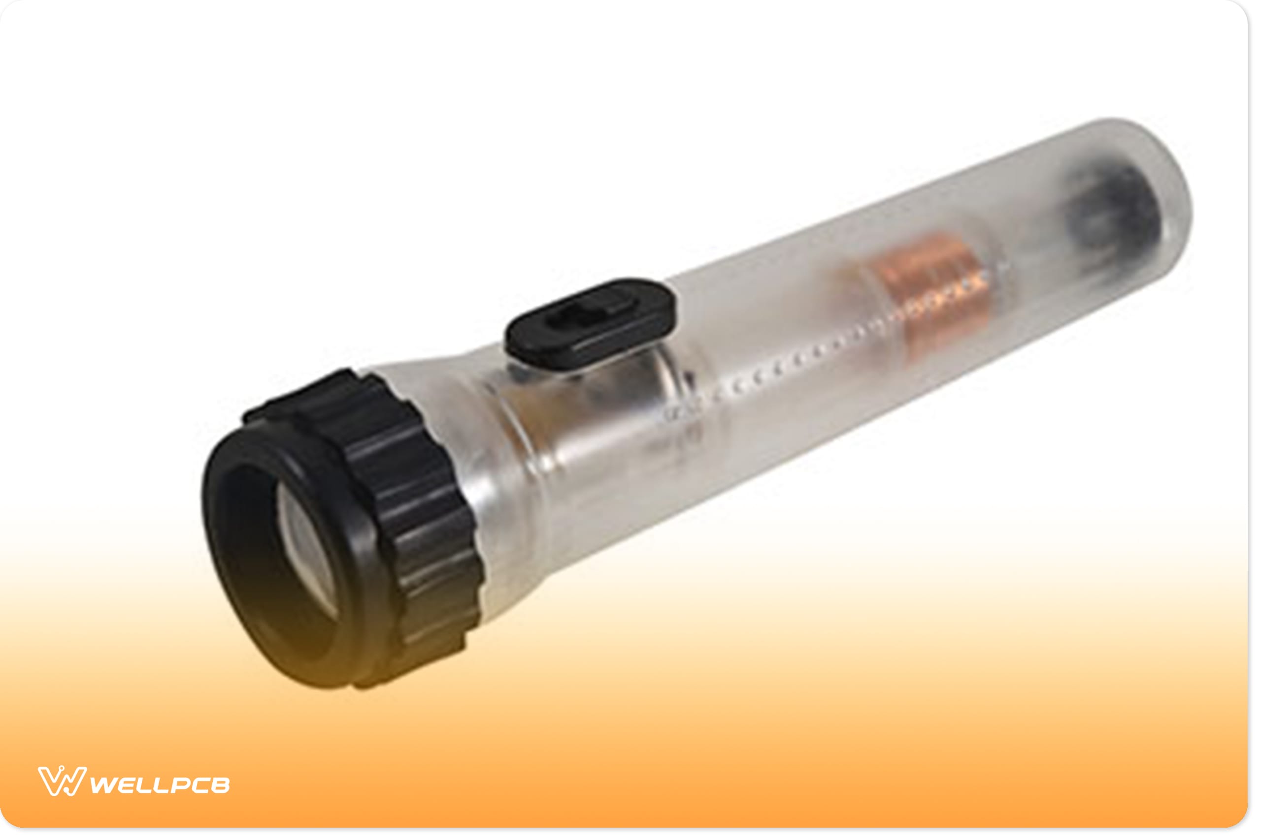
Farady Flashlight: Everything You Need to Know
Do you want to create a farady flashlight for your engineering project, but you have no clue about it?
Well, your search has come to an end—as this a...
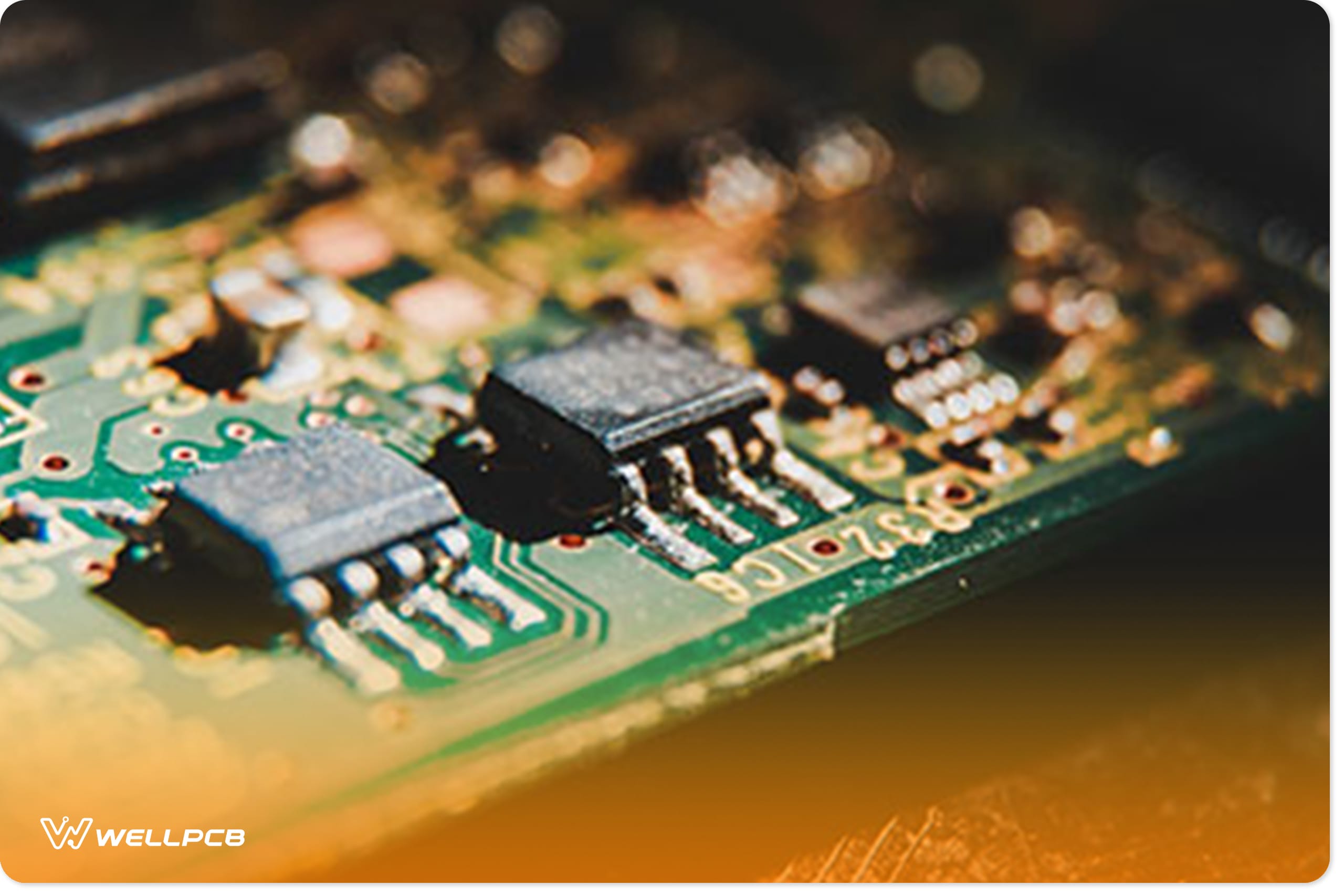
Test a MOSFET – How to Conduct an Effective Test
Test a MOSFET is a transistor type that uses voltage to regulate the degree of conductivity.
It belongs to field-effect transistors.
The level of t...

Remote Control Car Circuit: Everything You Should Know About It
A remote control car is one of the most popular toys for kids, and it’s hard to outgrow them as adults. Plus, the remote control car circuit is one of...
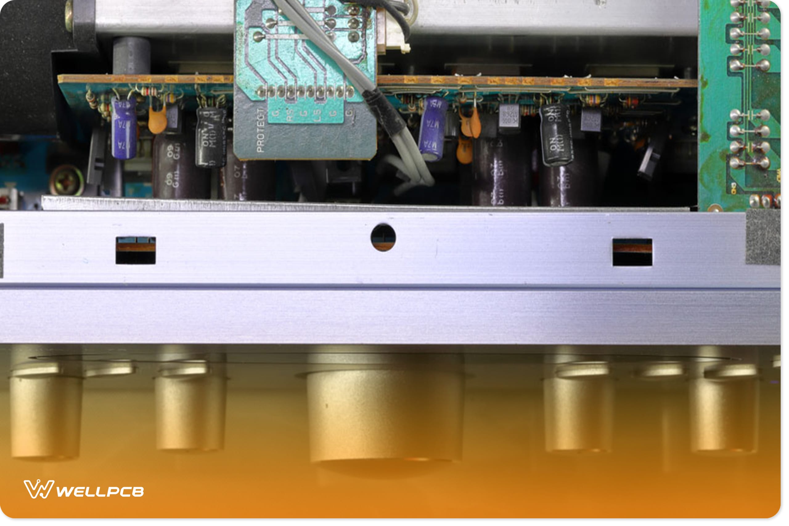
Volume Control Circuit for Speaker: Step by Step Guide to Enjoy Your Music
Today, we can play an audio signal on everything, but the speakers built into most devices leave something to be desired. Hooking up to external speak...

How to Build a Radio Repeater: A Complete Guide
The how to build a radio repeater is quite helpful for fixing communication problems. But do you need to build one for your project? Or do you need ad...
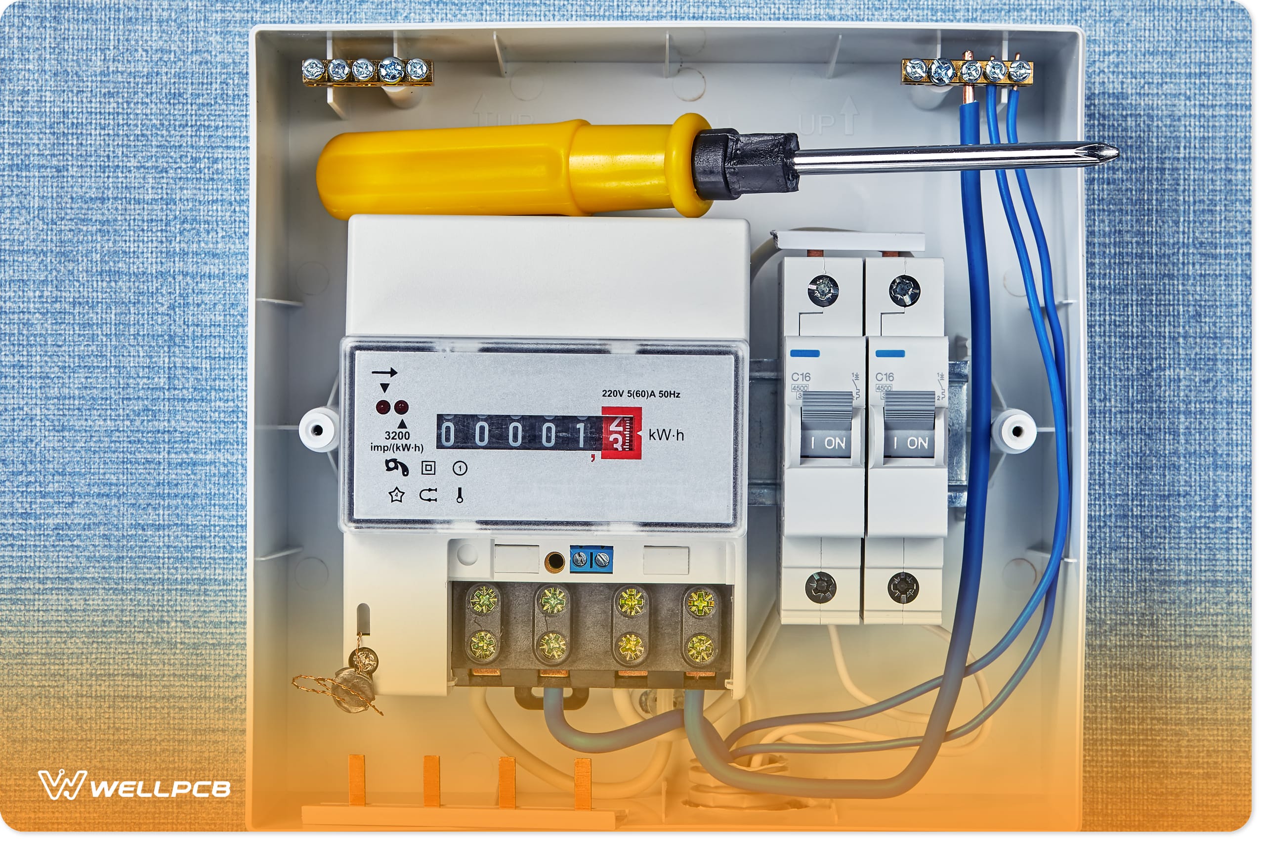
3 Phase to Single Phase Converter: 6 Methods (2026)
Converting from three-phase to single-phase is necessary for proper device functionality in small commercial and residential units. Plus, three-phase ...

Transistors in Parallel – The Ultimate Guide and Avoiding Mistakes
If a circuit draws in a lot of power, it will need a transistor to help regulate the current. However, an individual transistor may not perform the ta...
Transistor vs Resistor: What’s The Difference?
Mixing up terms or jargon is common in electronics, especially when talking about transistor vs resistor.
However, the issue does not just lie in how...
Battery Desulfator Circuit: A perfect solution for battery failure
Sometimes, we find ourselves facing a problem that affects our daily lives: a bad battery. The cause of this comes from natural sulfation buildup on t...

Taser Circuit – The Best Self-protection Device and How to Build One
Dangerous and lethal, a stun gun circuit stores voltage that, when hitting a target, causes severe pain.
Because of that effect, these provide stun ...
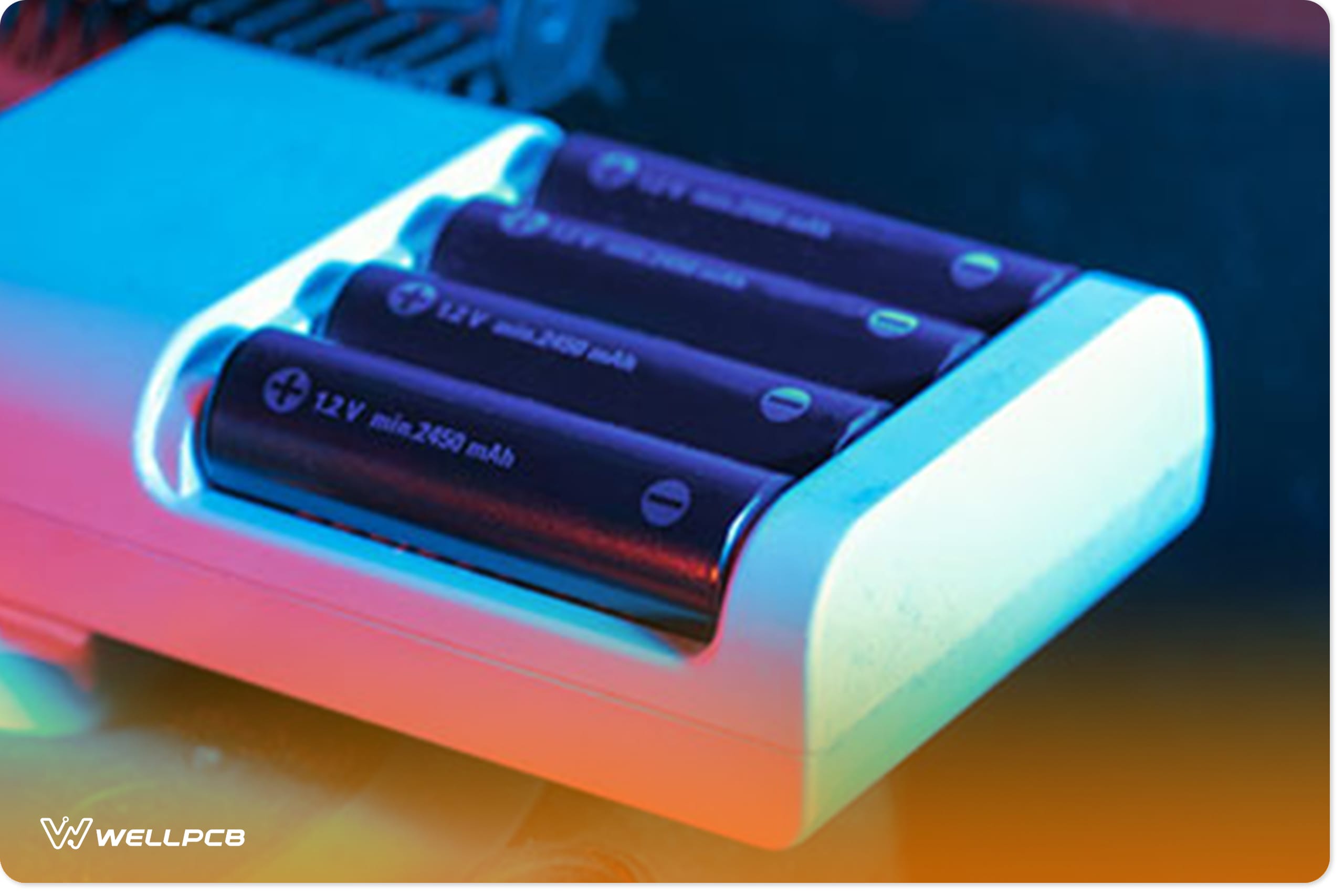
DIY Battery Chargers: The Complete Guide
The battery is one of the most brilliant inventions ever made. So, how it works is that it stores a fixed amount of power before running out. That's w...
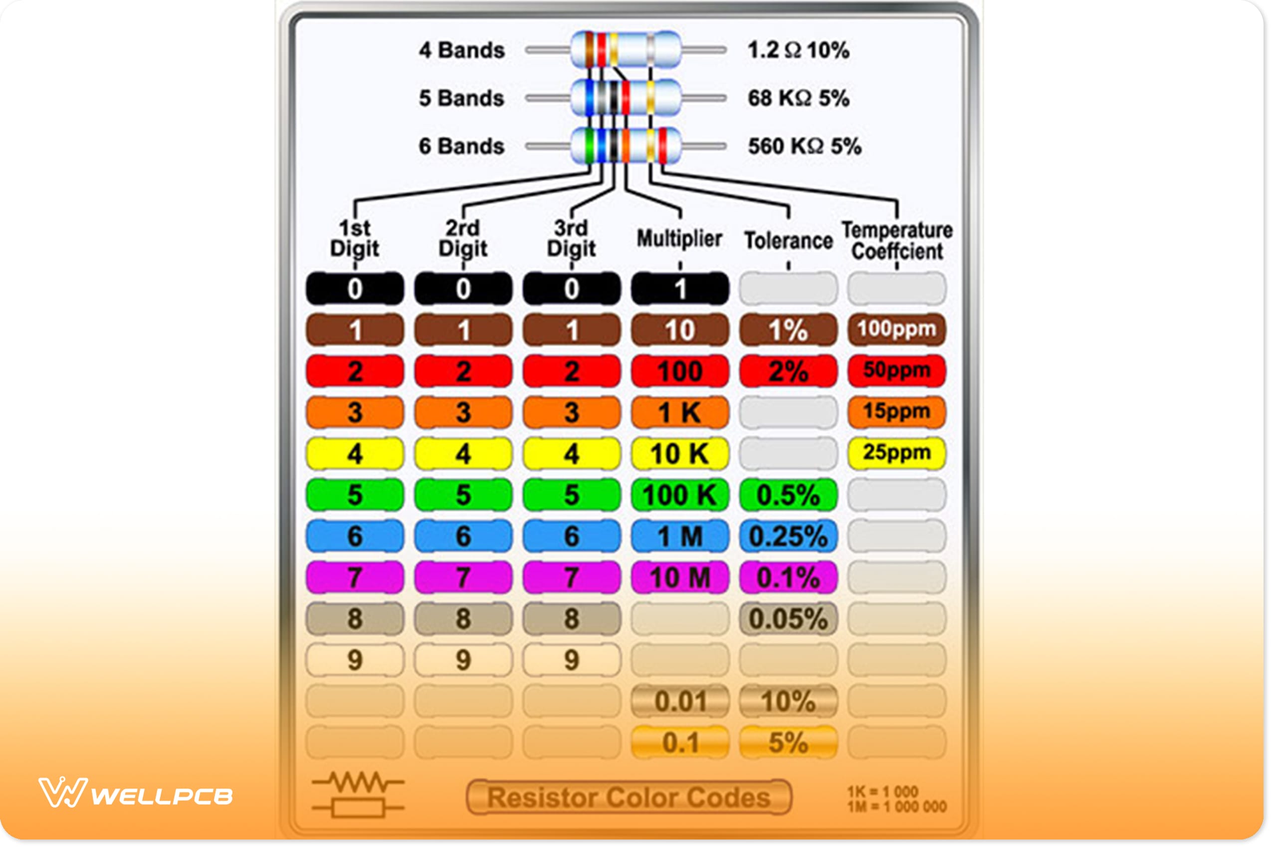
Resistor Values Chart & Color Code Guide – PCB Basics
Before you jump to resistor values, it's crucial to understand resistors.
Hence, a standard resistor is a device that goes against the flow of electr...
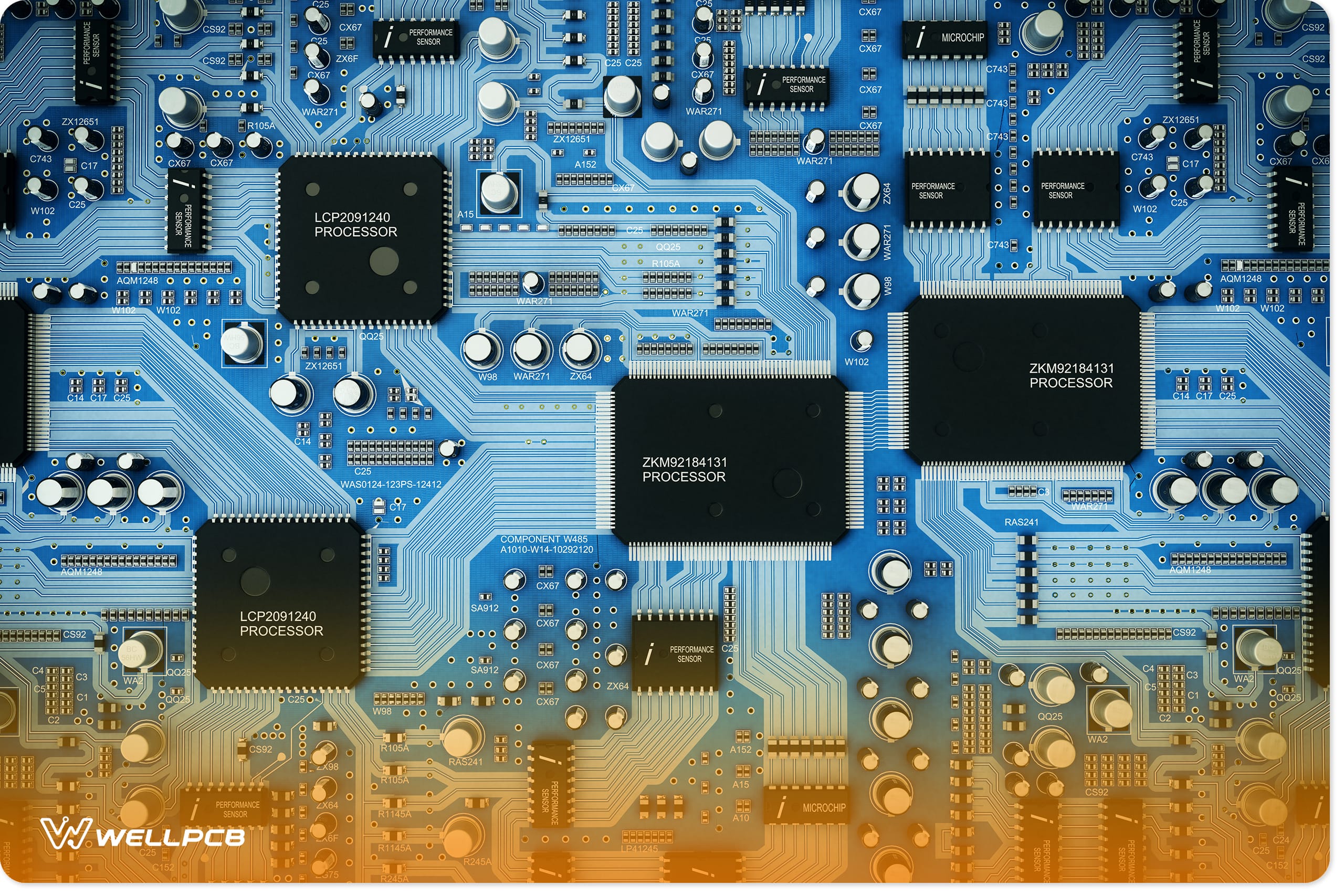
IC4017: A Beginner’s Complete Guide
Most DIYers and engineers prefer raw binary output over decimal coded output—in many cases.
In this regard, many available counter-integrated circu...
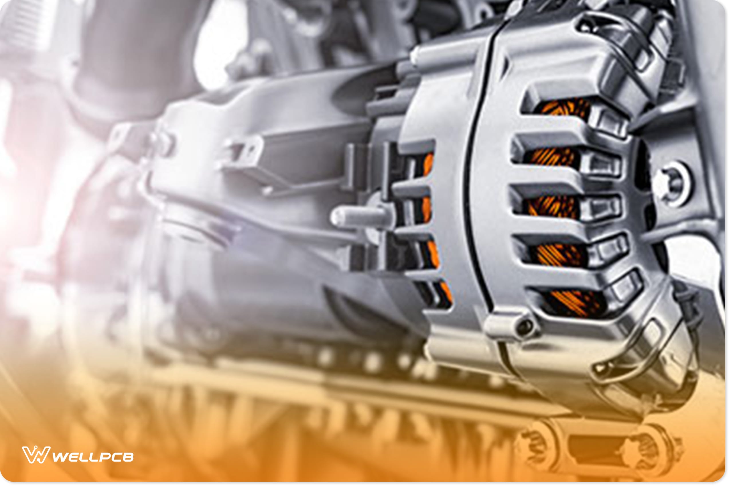
Self-Powering Generators: A Must-have Guide for the electronics industry
With the Do It Yourself (DIYs) era, who wouldn’t mind setting up a self-powered generator to run at their place of work or home? Besides being easy to...
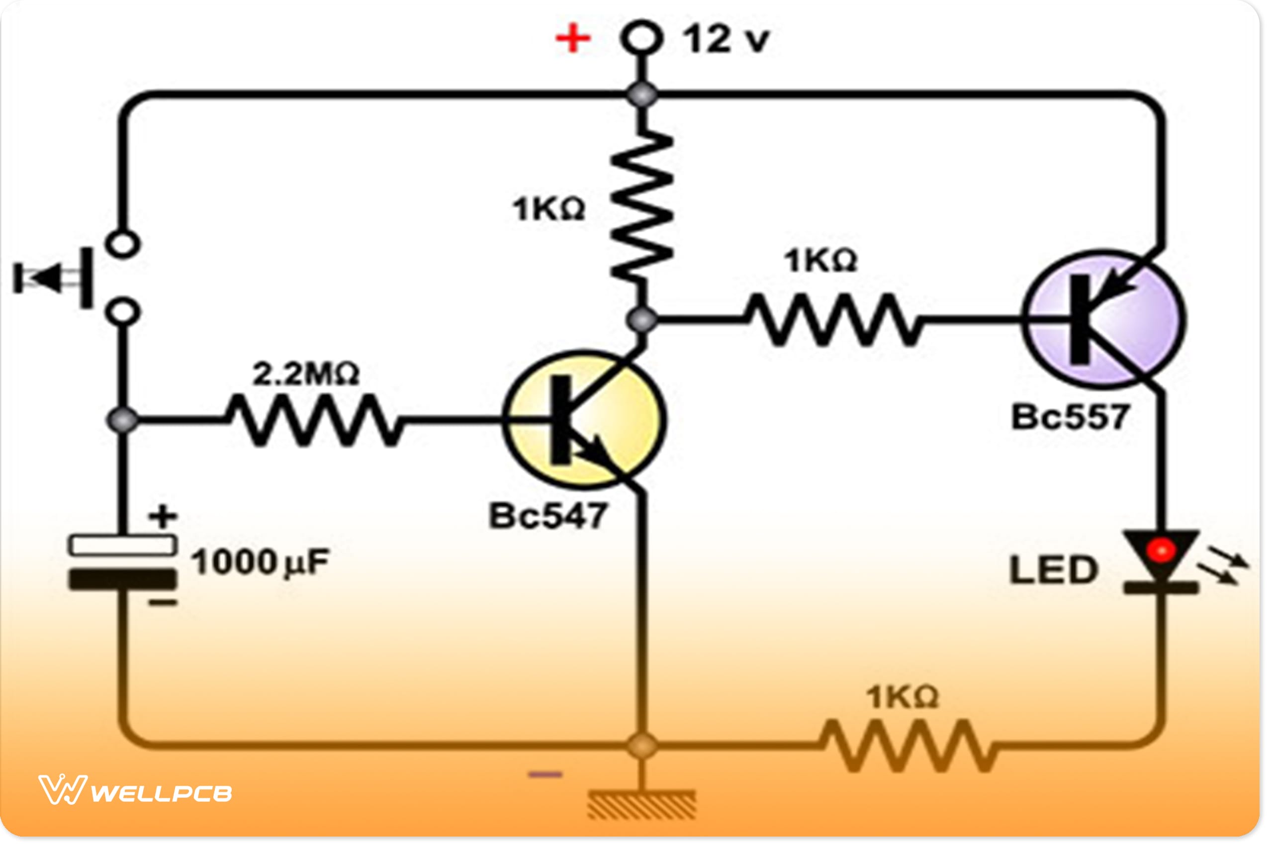
Timing Delay Circuit: Explaining a Time Delay Circuitry and its Applications!
If you’ve ever wondered what controls those pulsing airport lights, you’ve come to the right place! The answer, a time delay circuit, presents many ca...
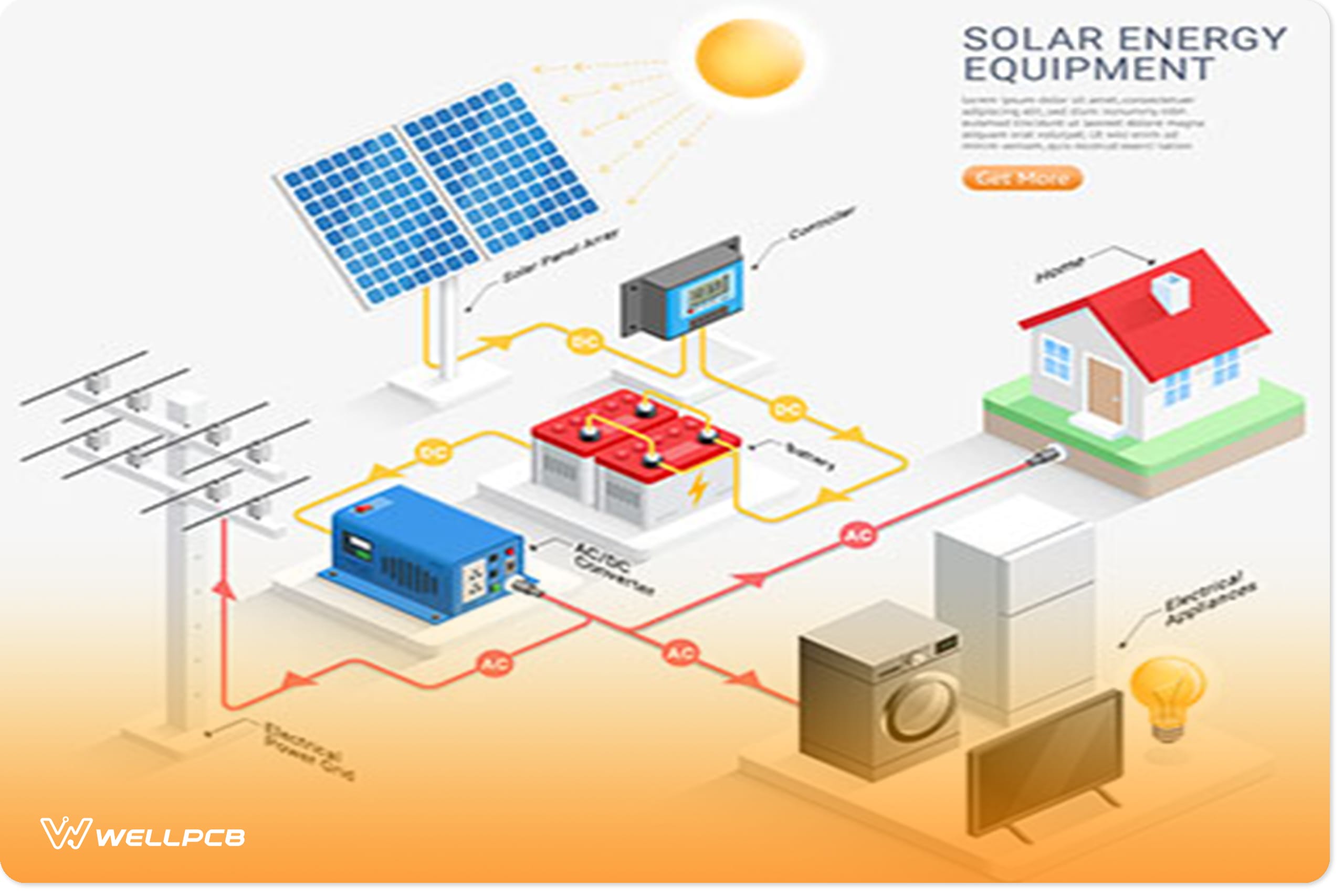
Inverter Circuit: The Ultimate Guide to Making Circuits at Home
The application of different electric power sources like DC battery storage alongside inverters is becoming common. In addition, inverter power source...
DIY Float Switch: Everything You Need to Know
Everyone would wish to make most of the operations done daily automatically. Besides, the same can be possible when trying to identify the water level...

Flexible Resistor: Everything You Need to Know
As electronic lovers, we’ve come across a wide variety of resistor cell exhibits ranging from fixed value resistors to large dependent resistors. Also...
PCB Milling: How To Make
PCB milling removes copper areas from a sheet of printed circuit board material. Depending on the digital circuit board, pads, structures, and signal ...
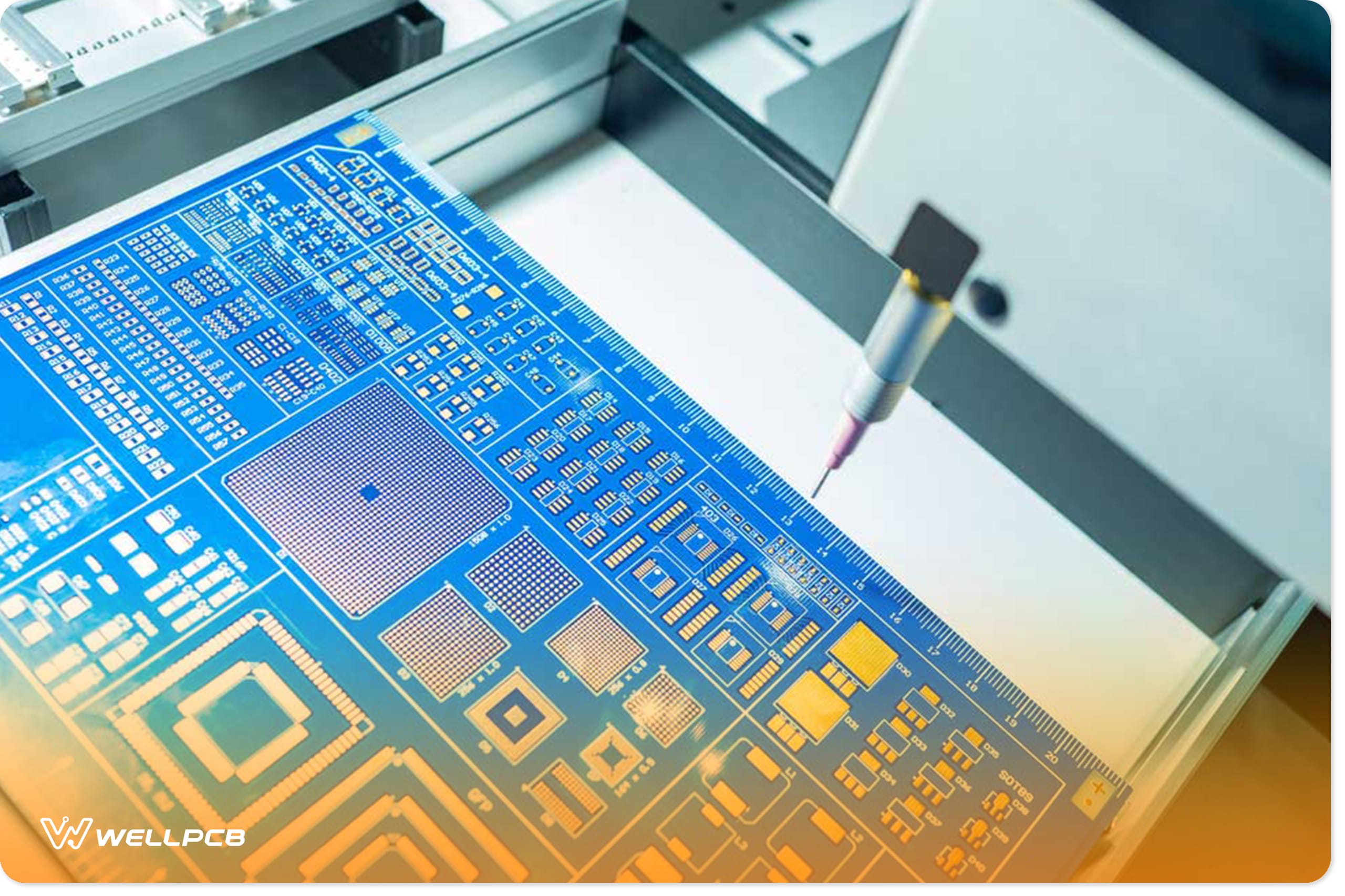
A Complete PCB Introduction It’s Here
PCB stands for Printed Circuit Board, a copper etched board that keeps printed the laid copper tracks. These tracks connect the components in most ele...
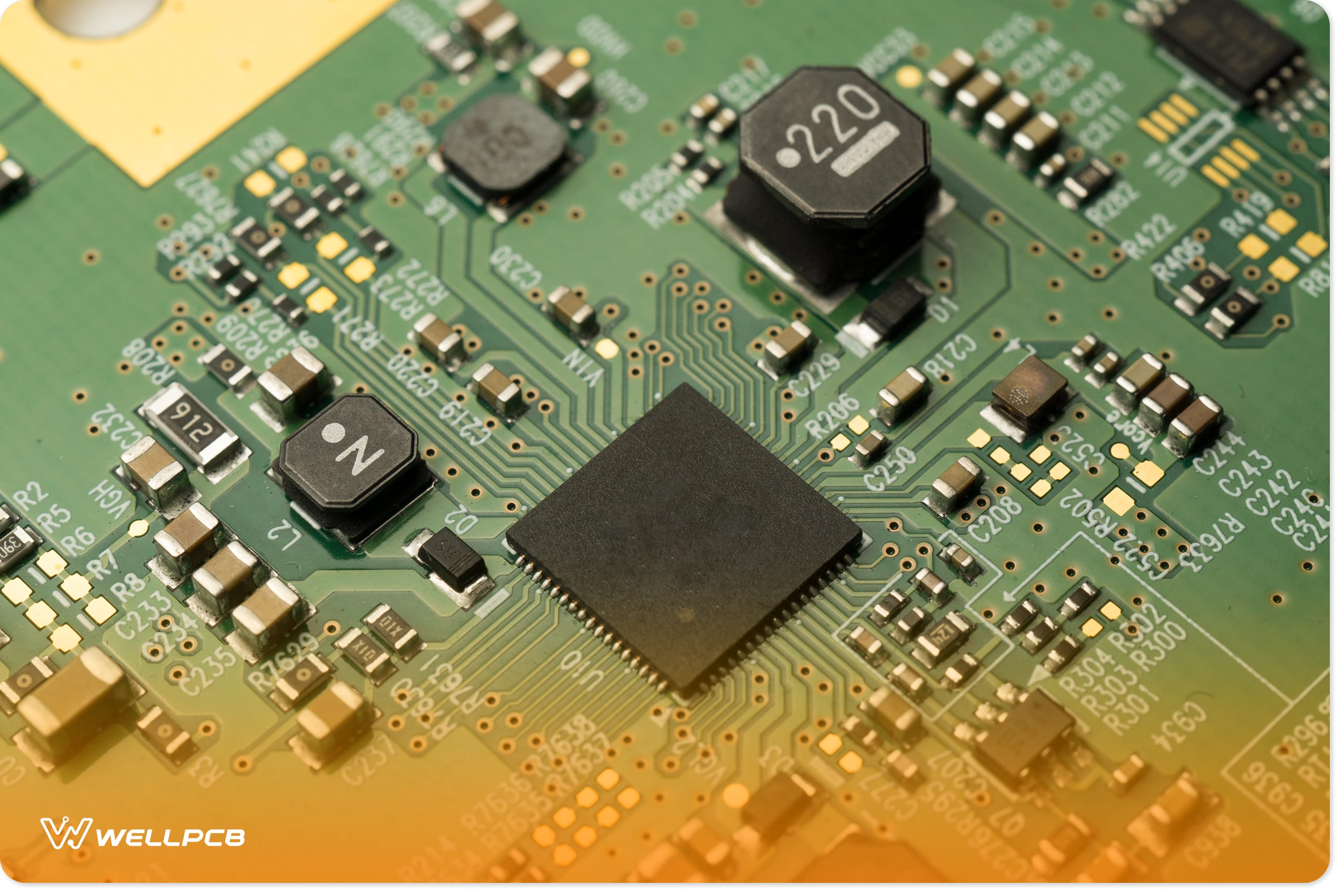
How To Design A PCB Layout(Helpful)
The printed circuit boards can be much more difficult to design if you are a beginner; however, learning the layout design of PCBs is not that difficu...

Power Supply Noise Decoupling in PCB Design
All electronic components transistors, analog, and digital ICs require power supplies for proper biasing. In most cases, the power supply rails (such ...

PCB manufacturing
Printed circuit boards (PCBs) shape the backbone of all significant electronics. These miraculous inventions pop up in almost all computatio...
PCB Wiring-How To( Easy Methods)
PCB Wiring is one of the most basic work skills of PCB designers. Whether it succeeds or not can directly influence the performance of the whole syste...
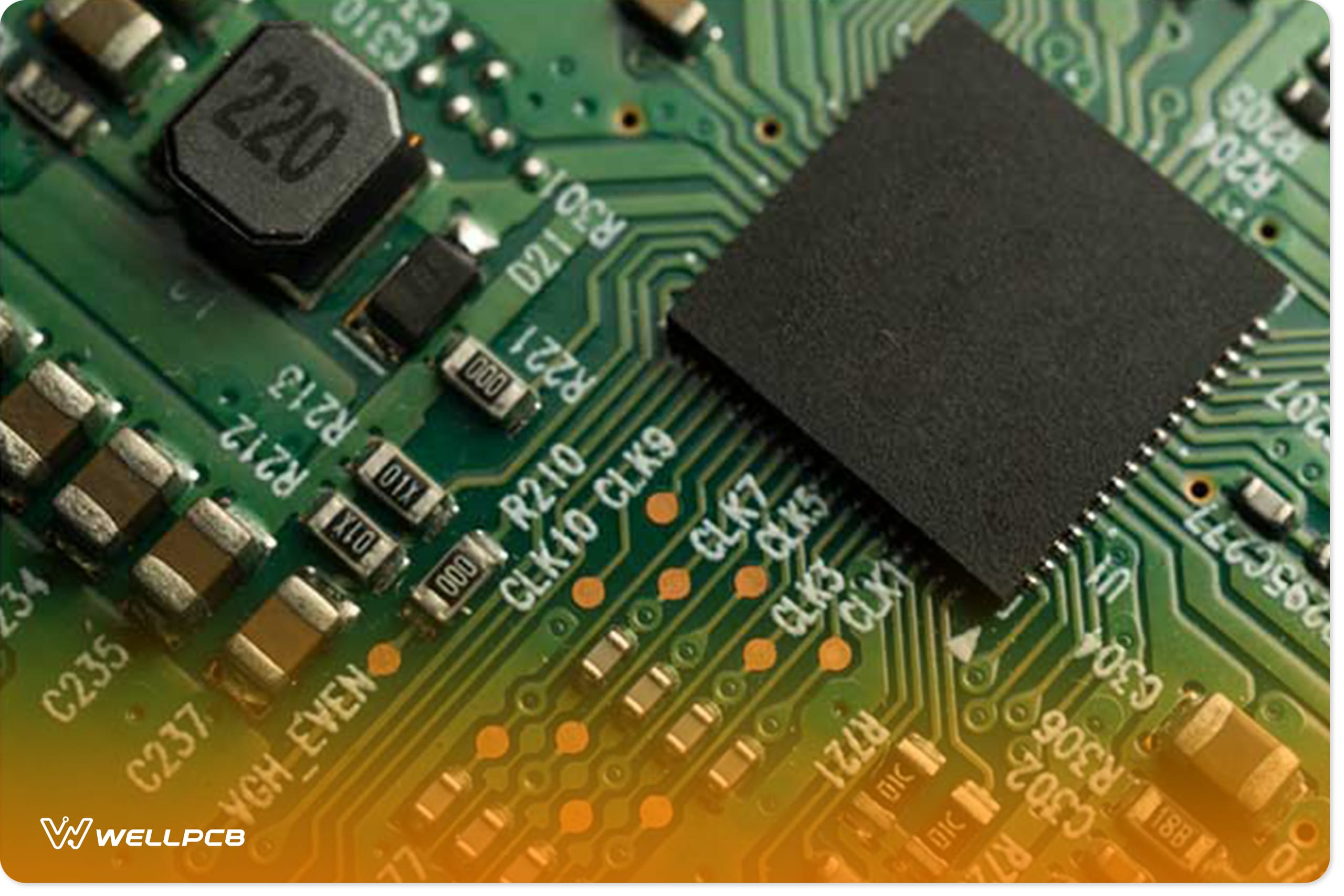
SMD – The Best Guide to SMDs and the SMT Technology
With the leaps and bounds experienced in this industry, various technologies come in place to manufacture these devices, and the Surface Mount Tech...
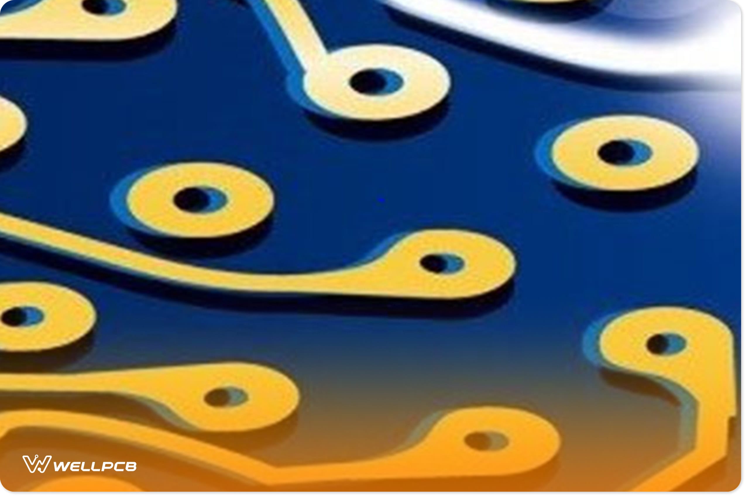
PCB Hole Size-How To Drill It-Quickly Review
To drill PCB hole size, you need to have the right tools. PCB drills are available to help make your work easier.
They vary in size, starting from 0....
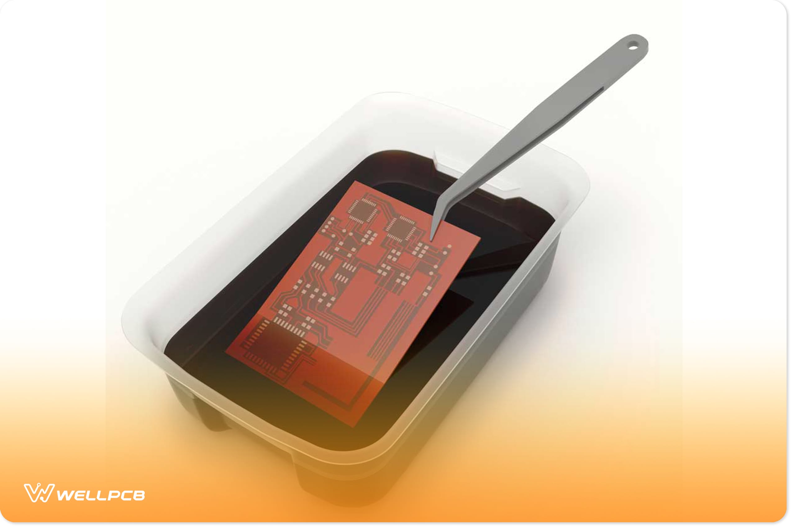
How To Make The Etching PCBs
Etching PCBs is a "subtractive" method used to produce printed circuit boards: acid is used to remove unwanted copper from a prefabricated laminate. T...

Gerber Files Creating with EAGLE (Free Ultimate Advice)
Gerber files are kind of a “universal language” for PCB designs. Most manufacturers accept it. So when you finish your design, you need to generate a ...
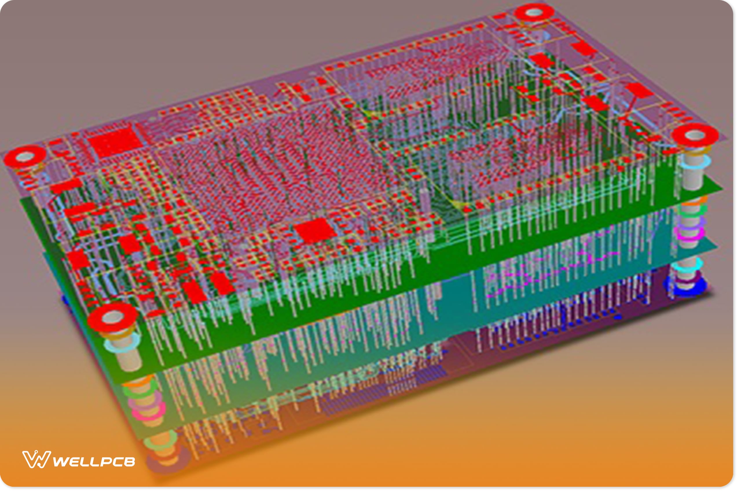
32-Layer Printed Circuit Boards: Techniques, Applications, and Benefits
A 32-layer printed circuit board is a multilayer PCB with 32 layers combined to function as one. Manufacturing this type of PCB isn’t possible with st...
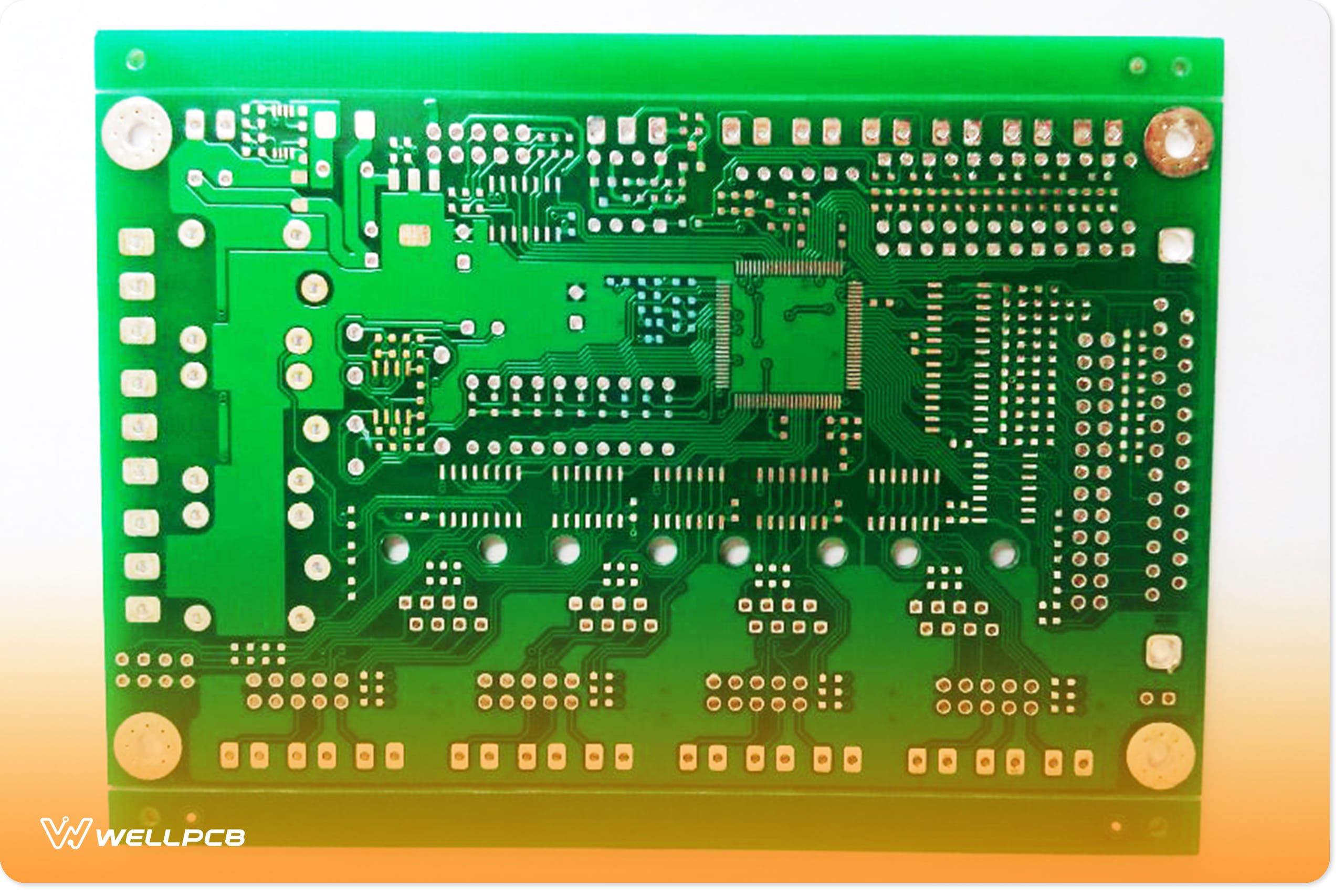
Photolithography Technology – The Most Useful Introduction
Photolithography is an important step in the process of creating semiconductor chips. The steps involve exposing a photoresist layer to light, develop...
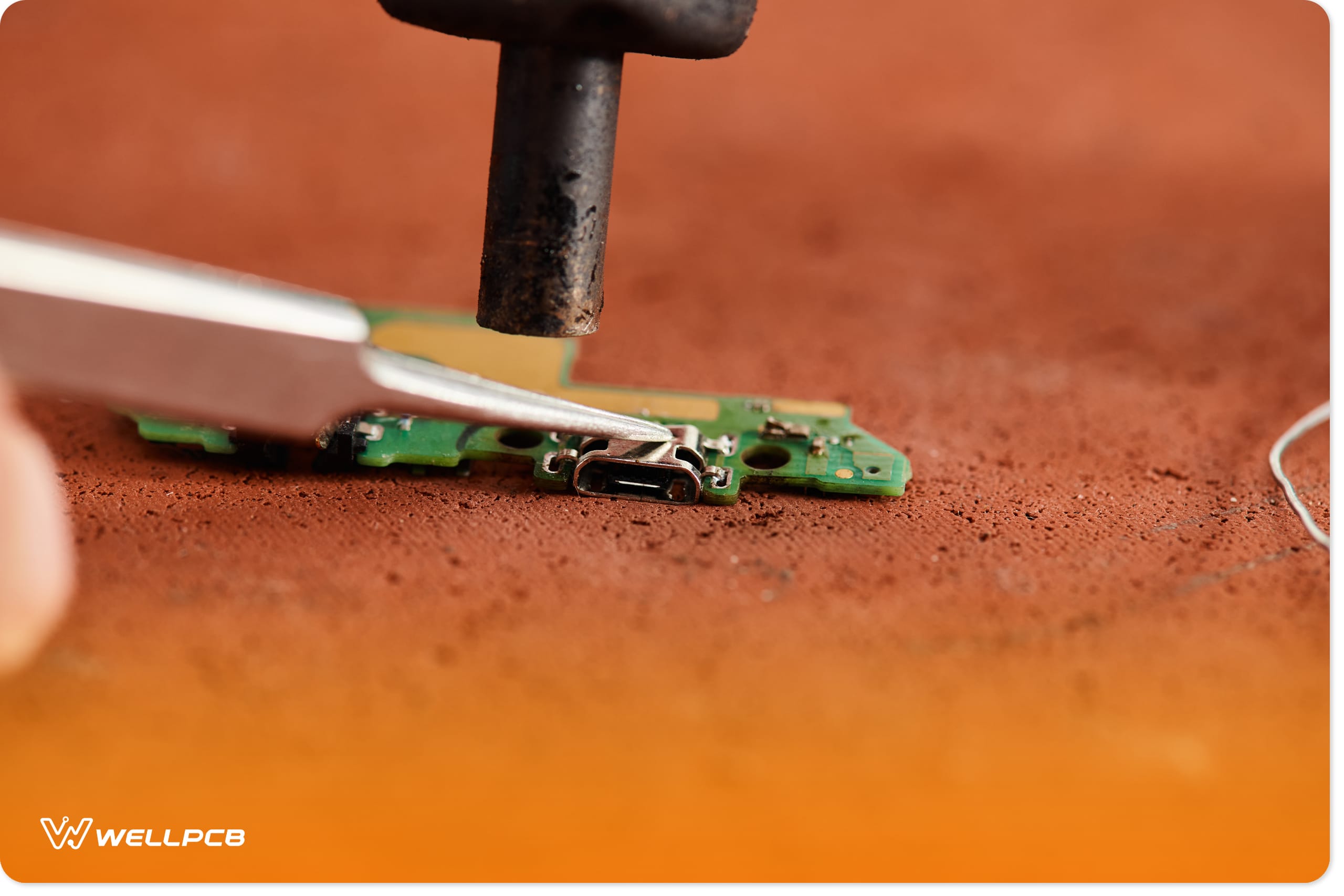
Desoldering and Solder Removal Techniques: The Ultimate Guide
A printed circuit board (PCB) often requires desoldering and solder removal to address excess solder on joints. Fortunately, the process is straightfo...

IP20 Devices: Introducing The IP Rating System
You will need to protect your electrical components or equipment from dust, dirt, moisture, or mechanical damage in some applications. But how do you ...
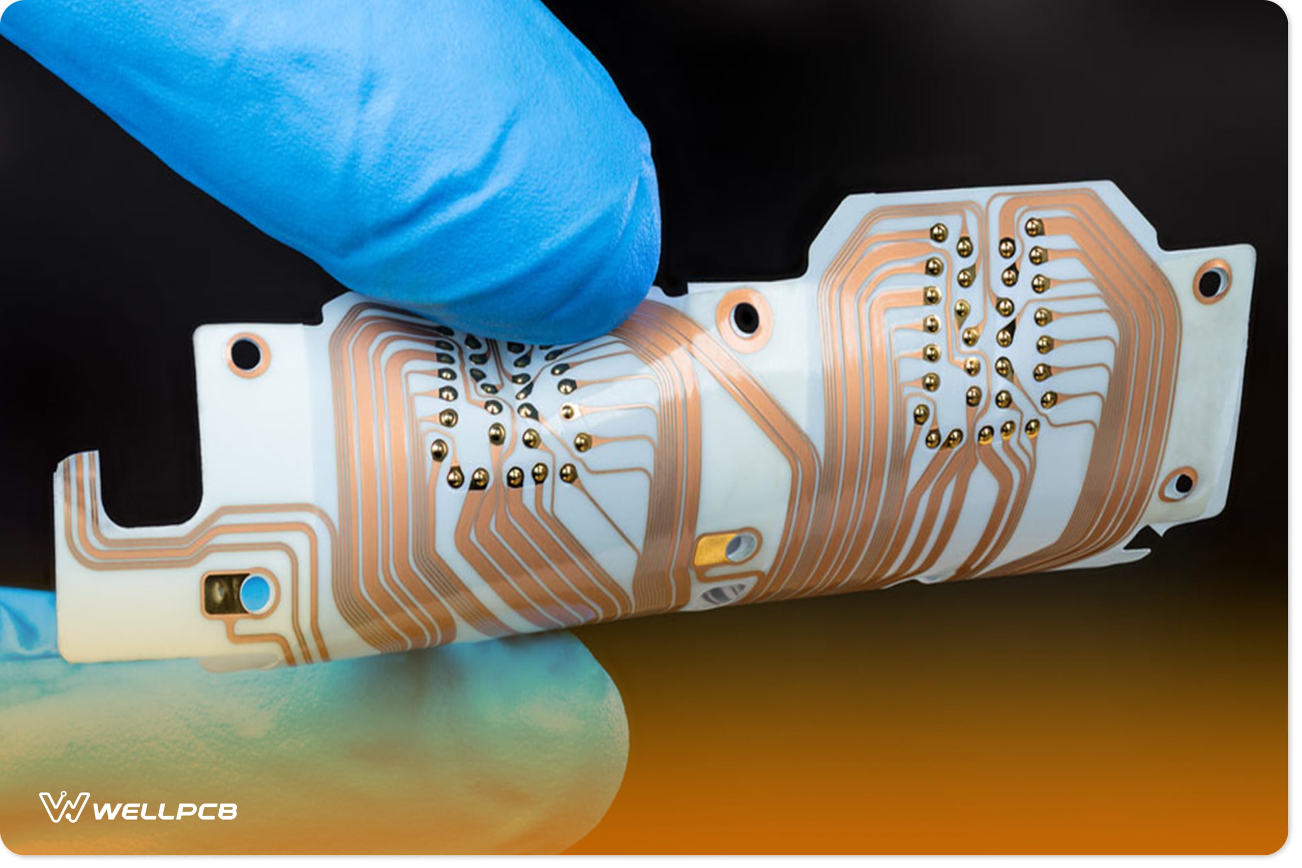
Spray Silicone Sealer: Your Right Choice for Electronics Application
Electronics systems use Spray Silicone Sealer to protect against moisture, heat, and UV light. This article will help you choose the right type of spr...
Thermal Adhesive: Bonding Electronic Components
Do you need to bond electronic components together but don’t know where to start? Using thermal adhesive puts you on the right track. It contains spec...

LED circuit board: 7 things you need to know
Light-emitting diodes have many advantages over standard lighting products. However, the light output of a single LED is relatively low. One way to in...

Fiducial PCB: Design and Function
Printed circuit boards (PCBs) are a vital component of most electronic and electrical devices. That’s why designers need to get it right when designin...
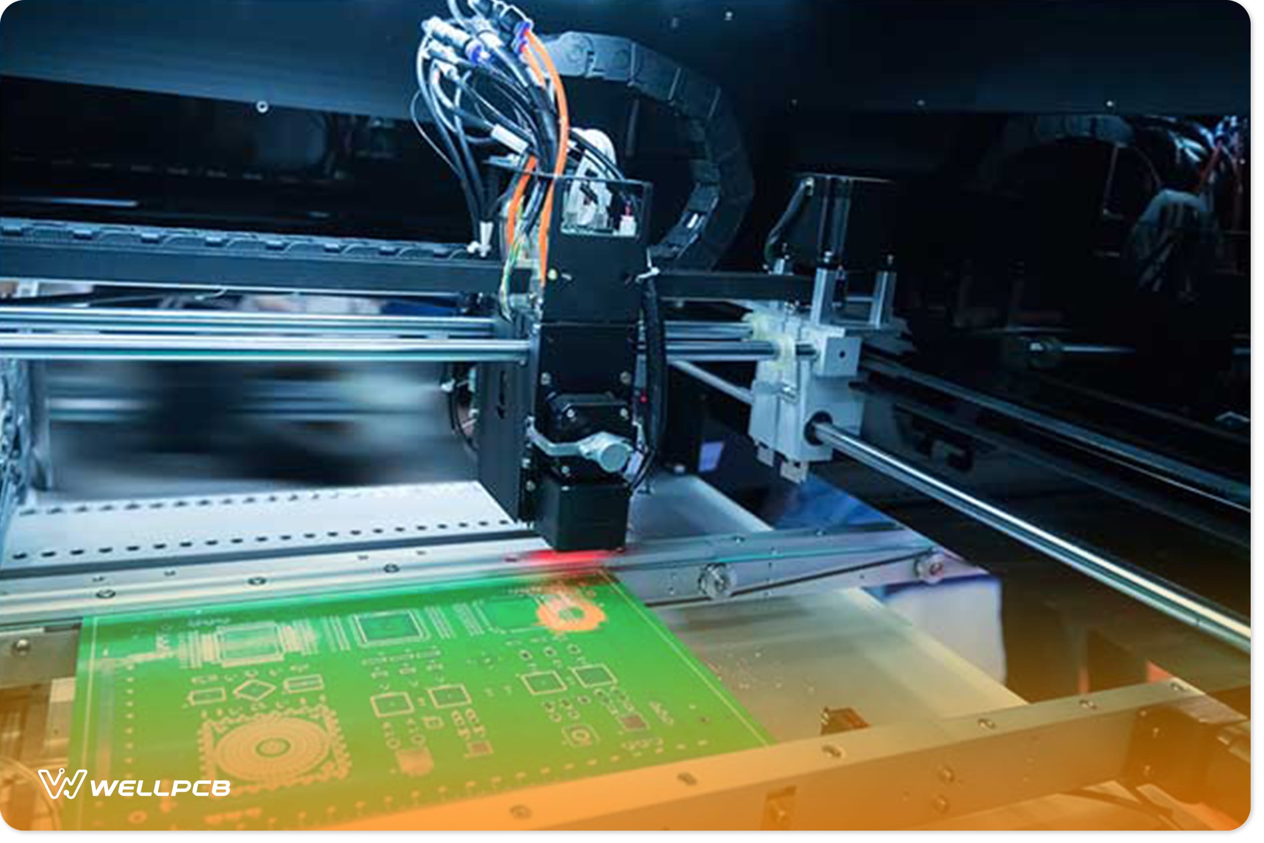
PCB Plating: The Complete Guide of Plating Techniques in PCB
What comes to mind when you hear the term "PCB plating"? Like many, you may assume it focuses solely on multilayer PCBs. In fact, you're not alone—man...
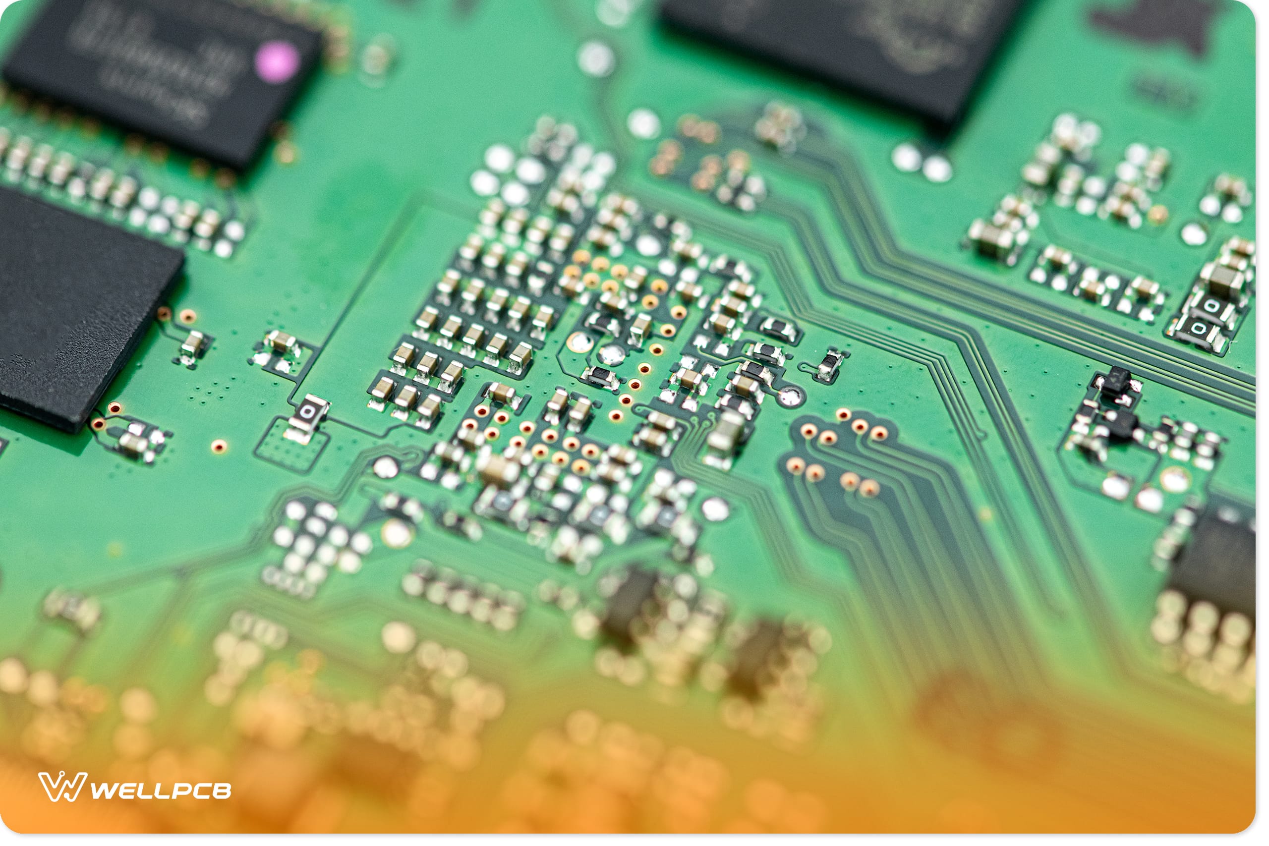
PCB Layers: The Ultimate FAQ Guide
Do you have loads of questions to ask about PCB layers? If yes, you’re in the right place.
PCB technology has come a long way.
So, designing a t...
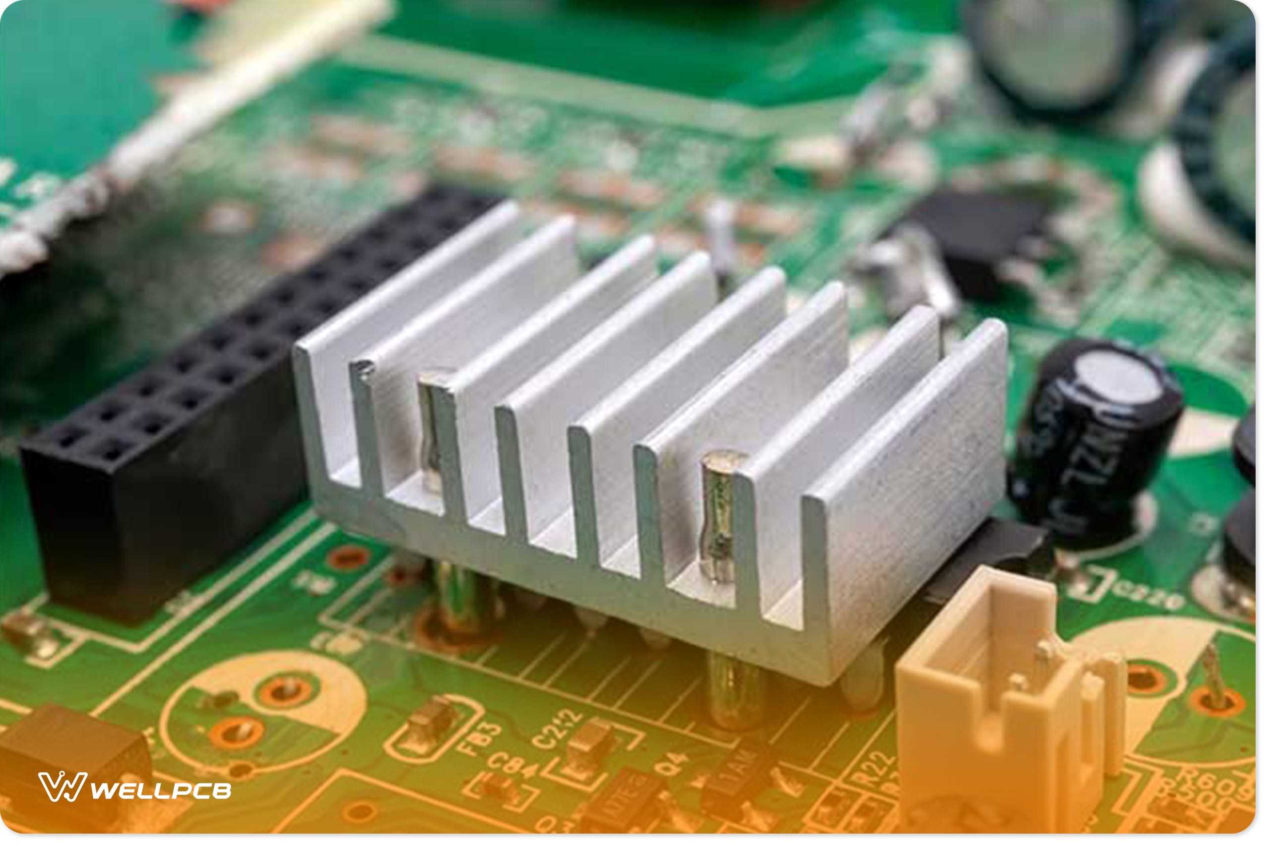
Aluminum PCBs: What Is It and Why You Need It?
Aluminum PCBs are components every PCB engineer should know.
The reason is simple.
Before now, most engineers depended on end-to-end wiring and conn...

6 Tips for Affordable Small Batch Assembly
A majority of PCB assemblers, especially small-batch manufacturers that are just starting t...
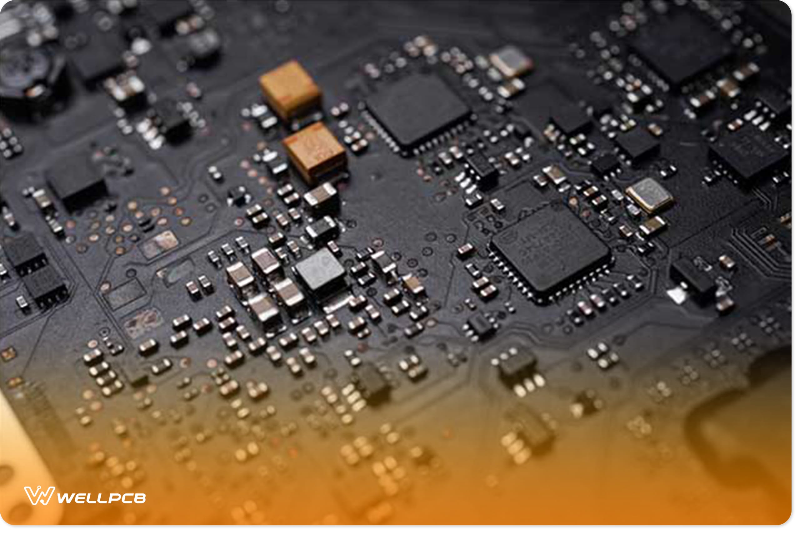
9 Ways to Get BGA Soldering on PCB in SMT Assembly
When it comes to SMT assembly, you may hear of people talking about BGAs or Ball Grid Array...
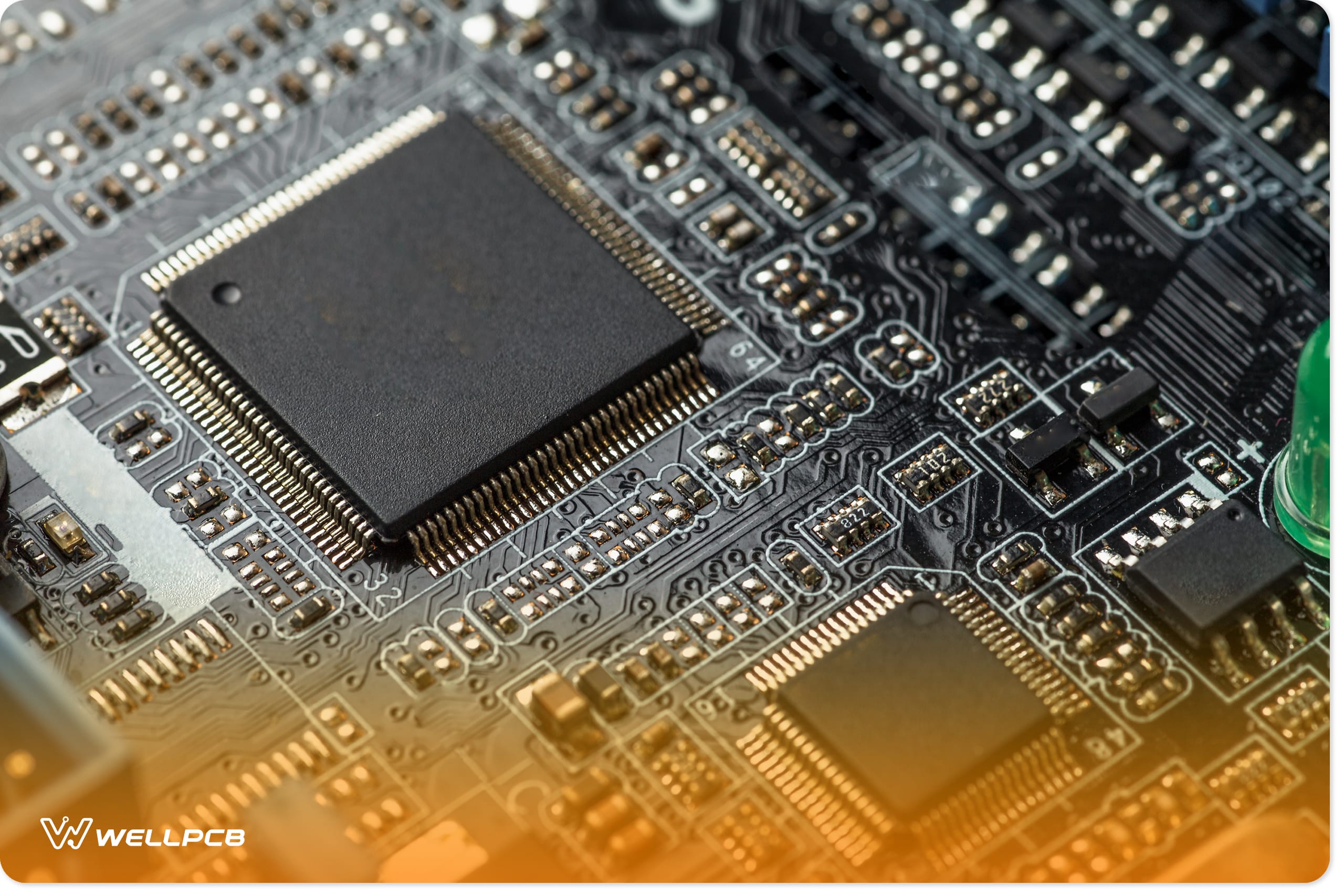
9 Common PCB Soldering Defects and Solutions
For more than two decades and counting, wave soldering has been relied upon by PCB designers for Read More
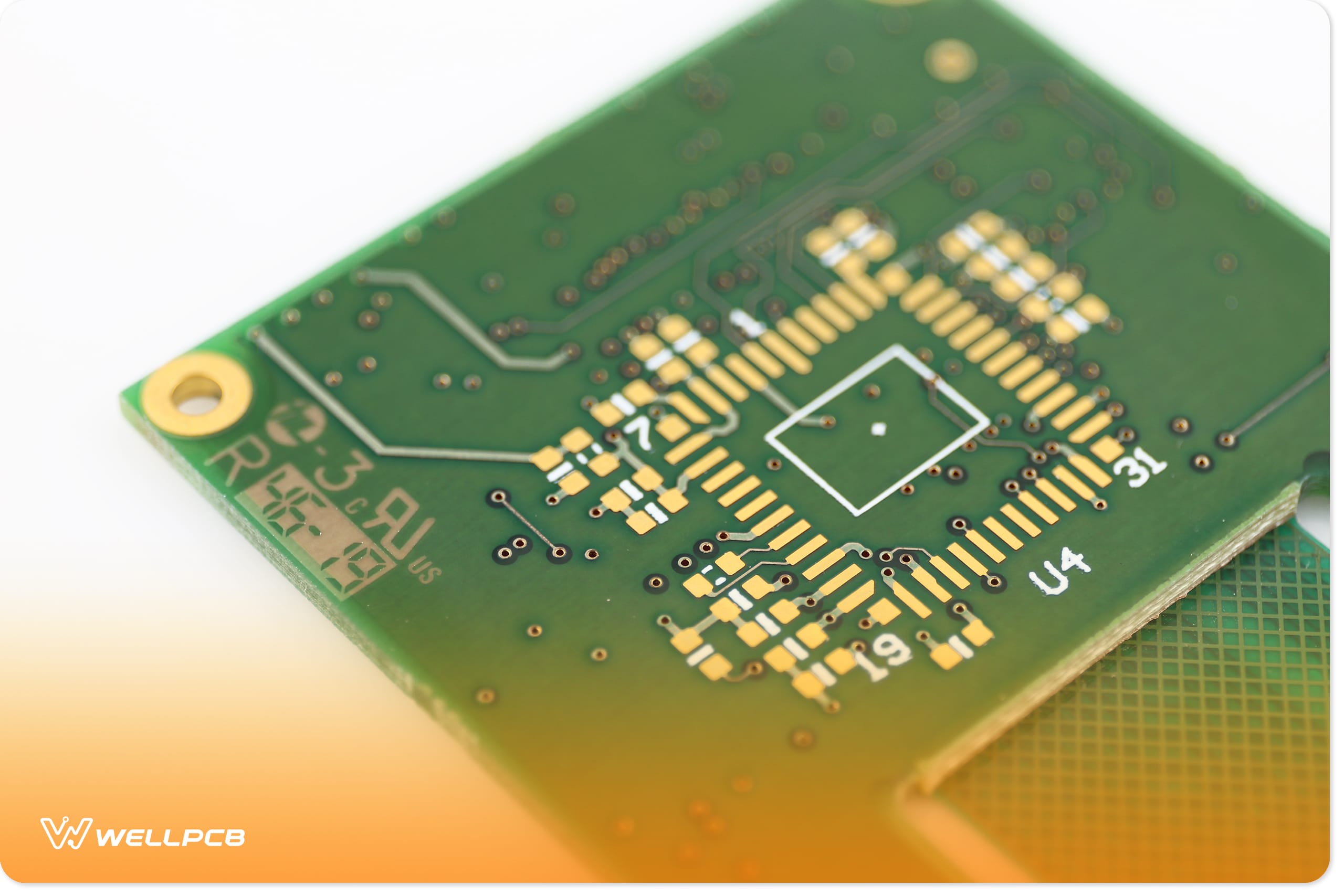
Custom PCB Printing-6 Things You Should Pay Special Attention
Printed circuit boards are indispensable units in nearly all electronic products that ...

5 Ways to Order Custom Printed Circuit Board Online
circuit board is your first bet when trying to come up with a prototyping circuit.
They minimize space and realize edgy efficiency is a plus for mos...
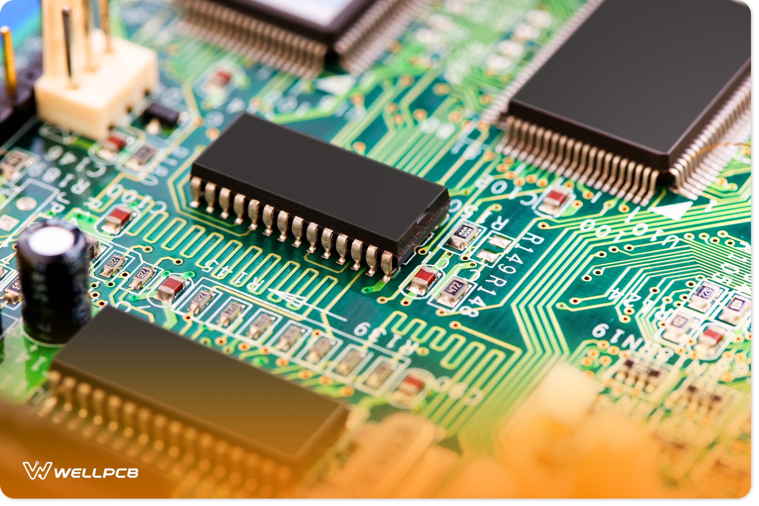

10 Things You Need to Know About PCB Assembly Costs
PCB assembly cost include the cost of labor, turnaround time, technology, and the quantity of PCBs needed. Technicians and engineers alike often wo...
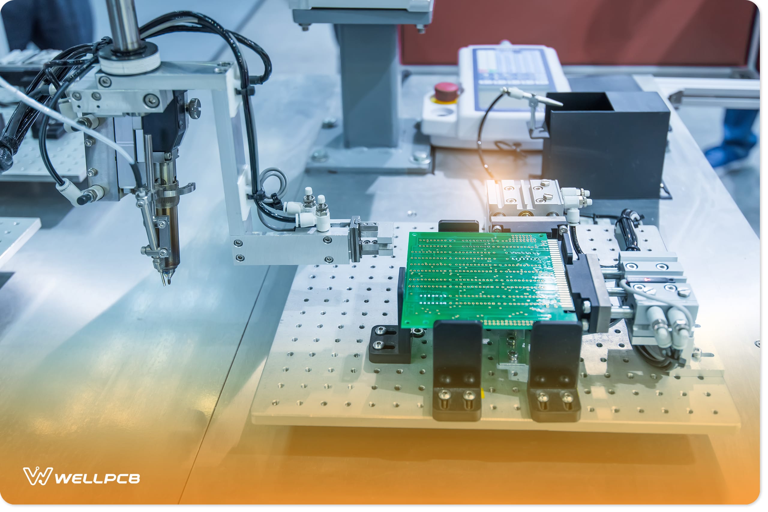
5 Years of Experience Sum up 10 Ways to Choose a PCBA Company
If this is your first time working with PCB, you must be in deep waters and unable to find the right provider.
Most people choose to work with compan...

7 Reasons for Businesses Turning To Small-Batch PCB Manufacturers
We live in a world where almost everything that we use has a printed circuit board in it. With this, more and more business entities are beginning to ...
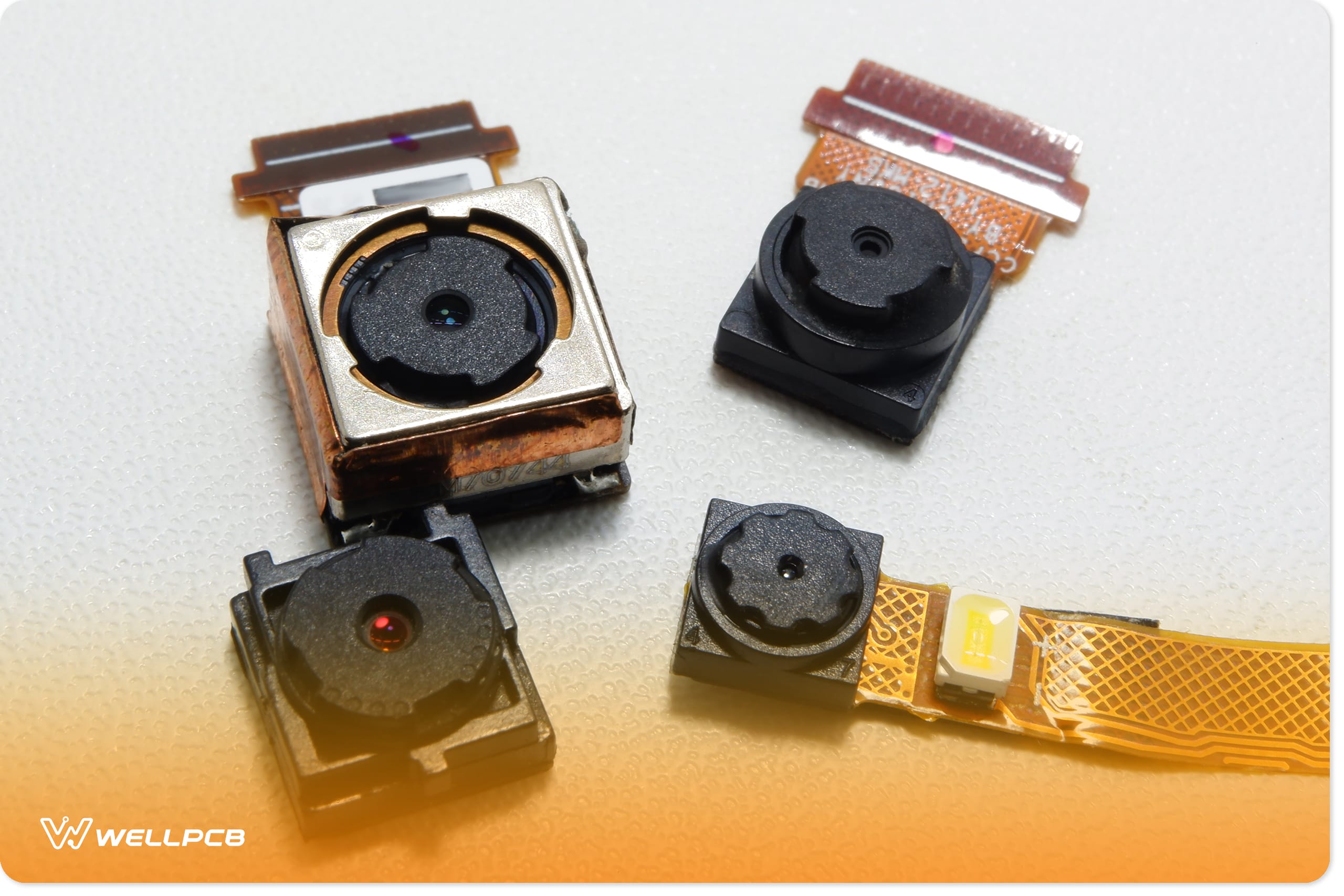
9 Ways to Make Flexible PCB Manufacturing Process Perfect
You can follow several ways to make the process of manufacturing flexible printed circuit boards perfect. While they all work out, some could turn out...

10 Comparison Aspects Of Rigid and Flex PCB
Printed circuit boards connect electrical components in one place through discreet wiring, an aspect that results in a functional and complete unit. P...
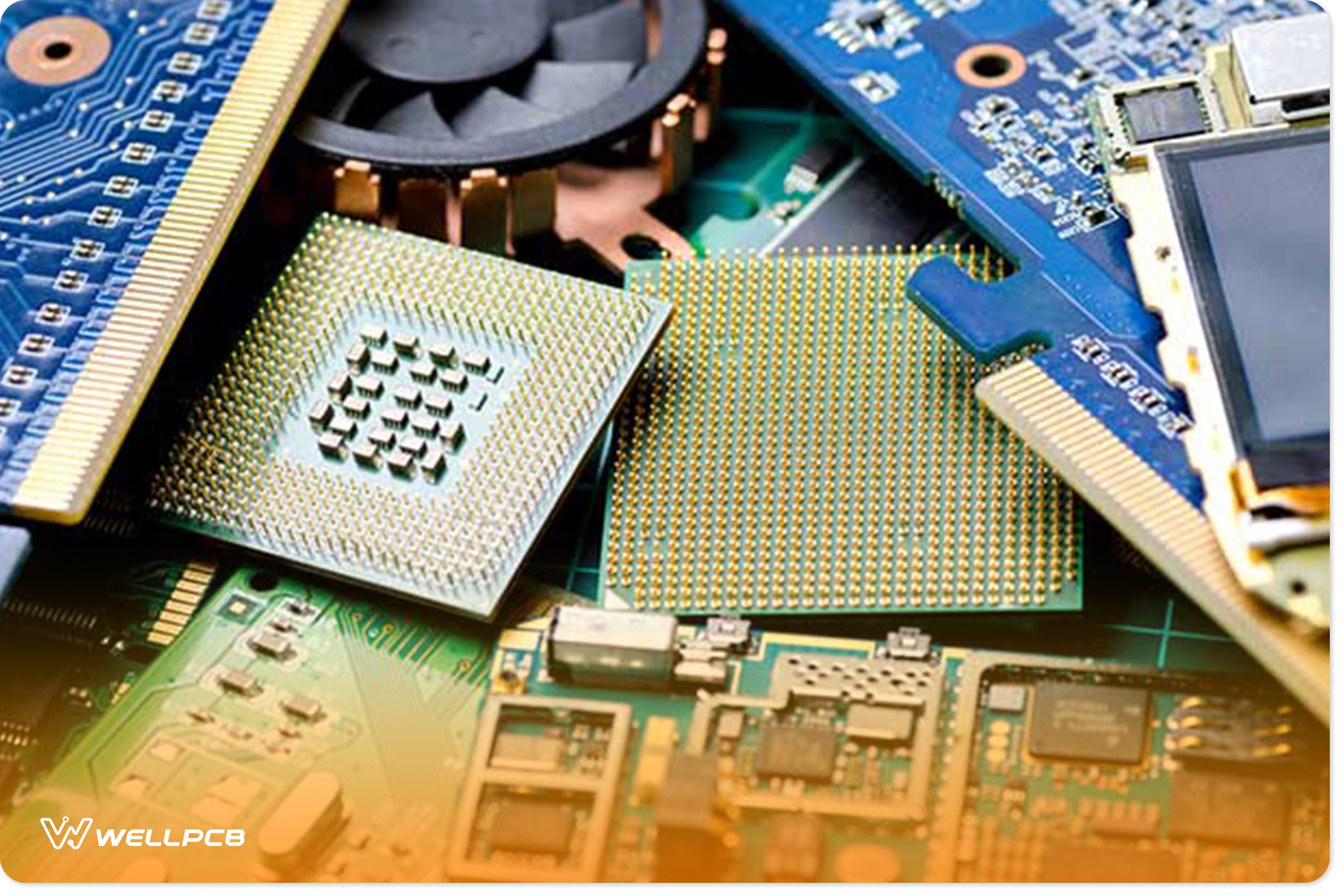
9 Useful Ways To Help Build a Custom PCB Easier
If you are looking to make permanent electronics projects, then using the traditional breadboards for prototyping is not a good option. The earlier yo...
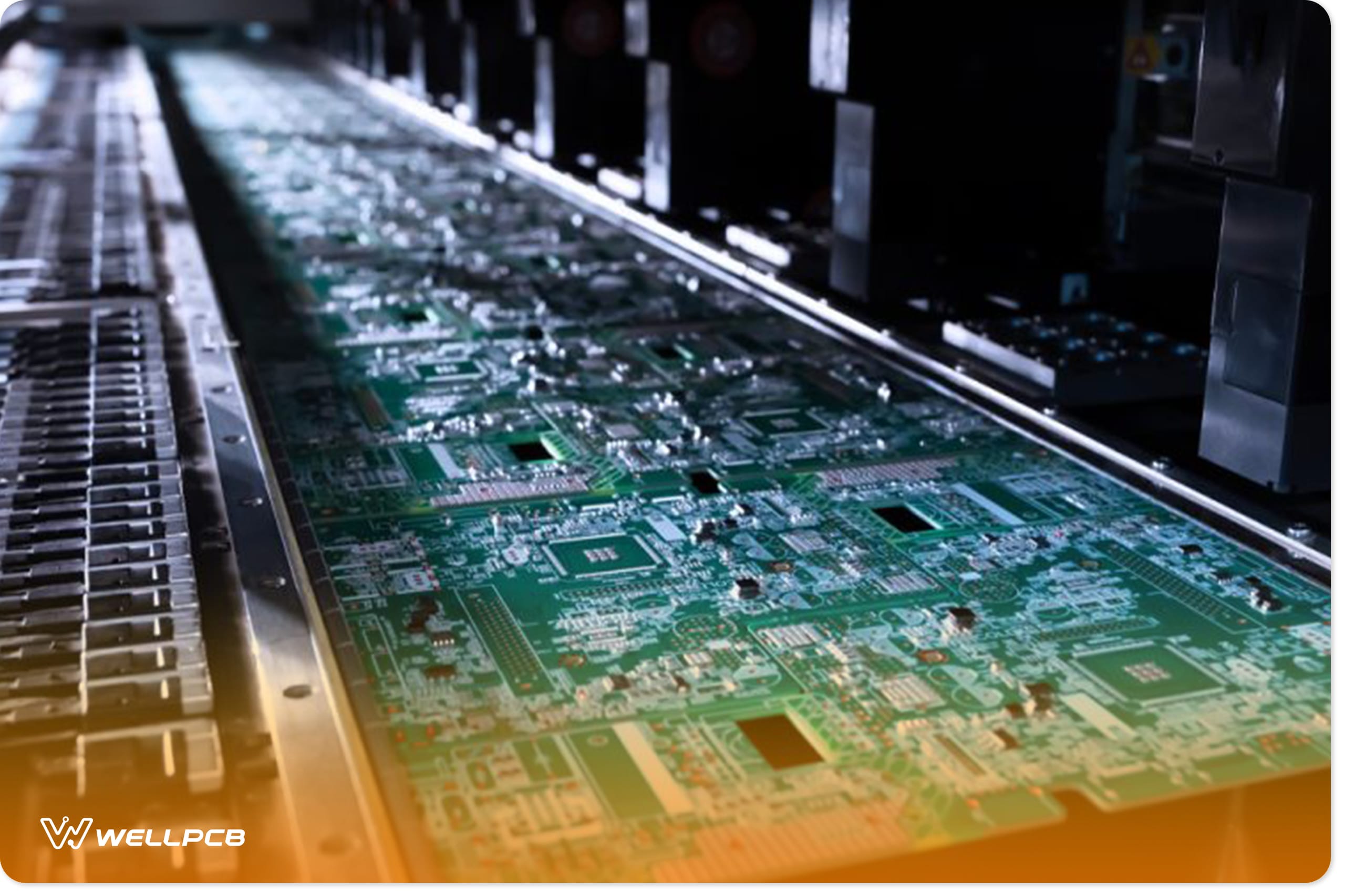
Big Advantages of China PCB Manufacturer
As a world titan in many markets, China is also a leading electronics manufacturing business.
China's PCB manufacturer is famous for producing innov...

A Comprehensive Guide To Building Digital Circuits
Digital circuits or digital electronics are electronics that use digital signals. They’re different from analog circuits in that analog circuits opera...
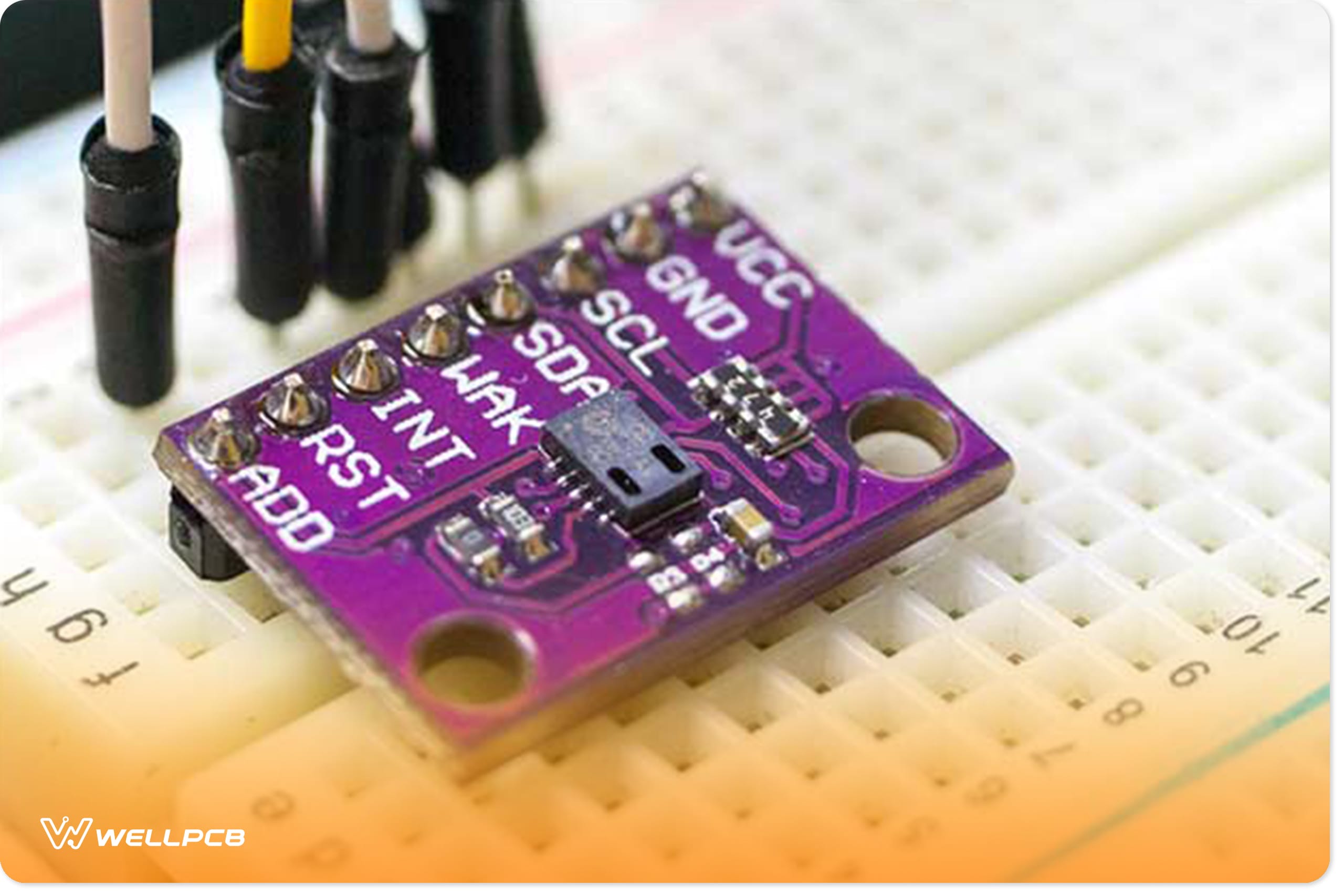
6 Steps To Understand The Solder Mask
How do you prolong the life of a PCB? It would help if you had a protective coating to avoid oxidation. This is the role of the solder mask! However, ...

How to Design a PWM Circuit You Need
There are several different ways of controlling the speeds of DC motors. However, one of the most preferred and simple ways is by using a Pulse Width ...
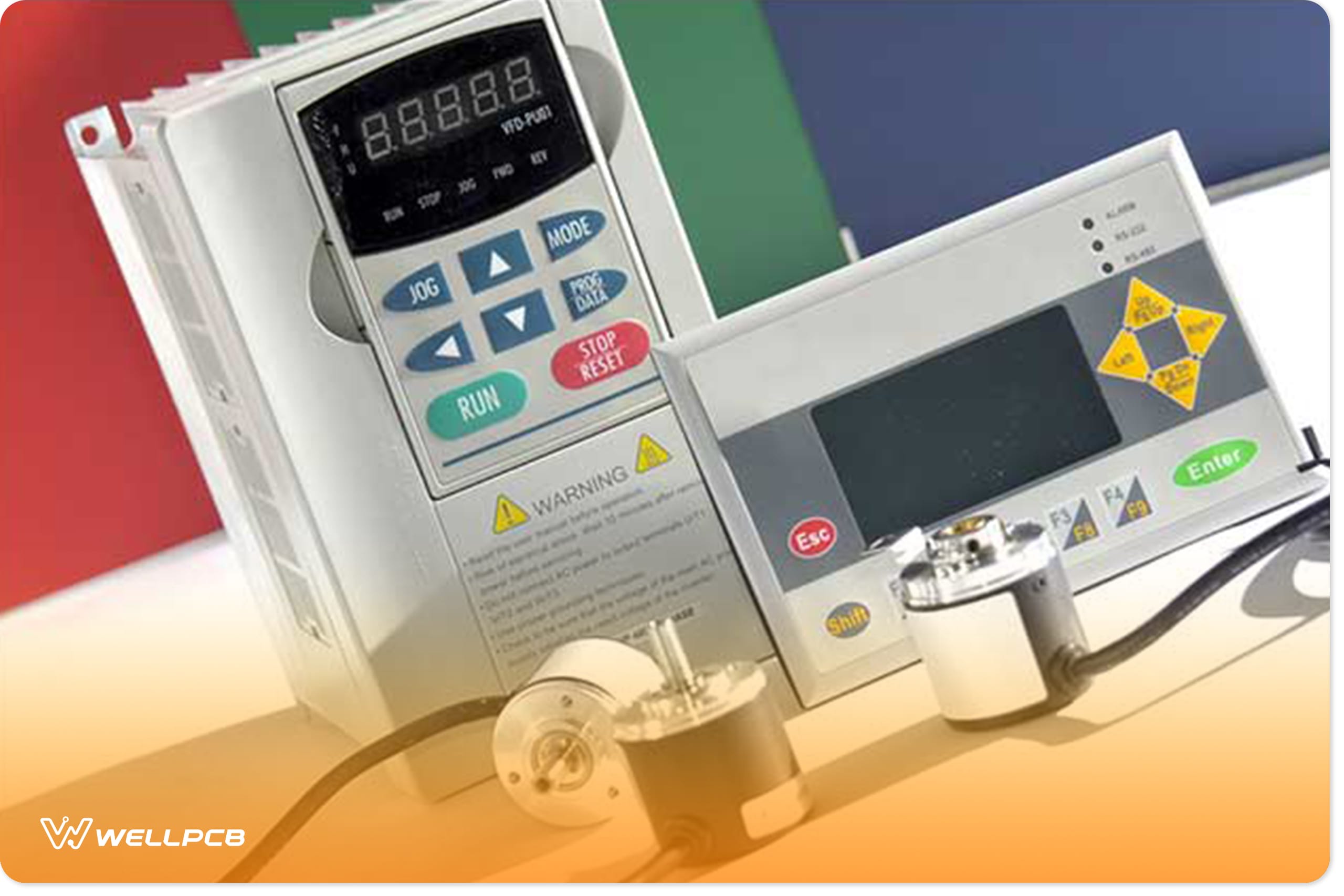
Find Motor Controller Failure Reasons
A motor controller is a handy device that has the task of regulating that the motor performs optimally, and within the predicted capabilities. However...
Flexible Rigid PCB – How to Make its Assembly Look Simpler And More Reliable
Do you want to try Flex-rigid PCB, but you are afraid of the potential performance issues and problems during the assembly process?
As long as you en...
Rogers PCB – The Ideal Component for Efficient Circuit Boards
You must have heard about PCB if you are new to engineering or technology. But what does PCB mean? Why is Rogers PCB so popular?
Read ahead to find ...
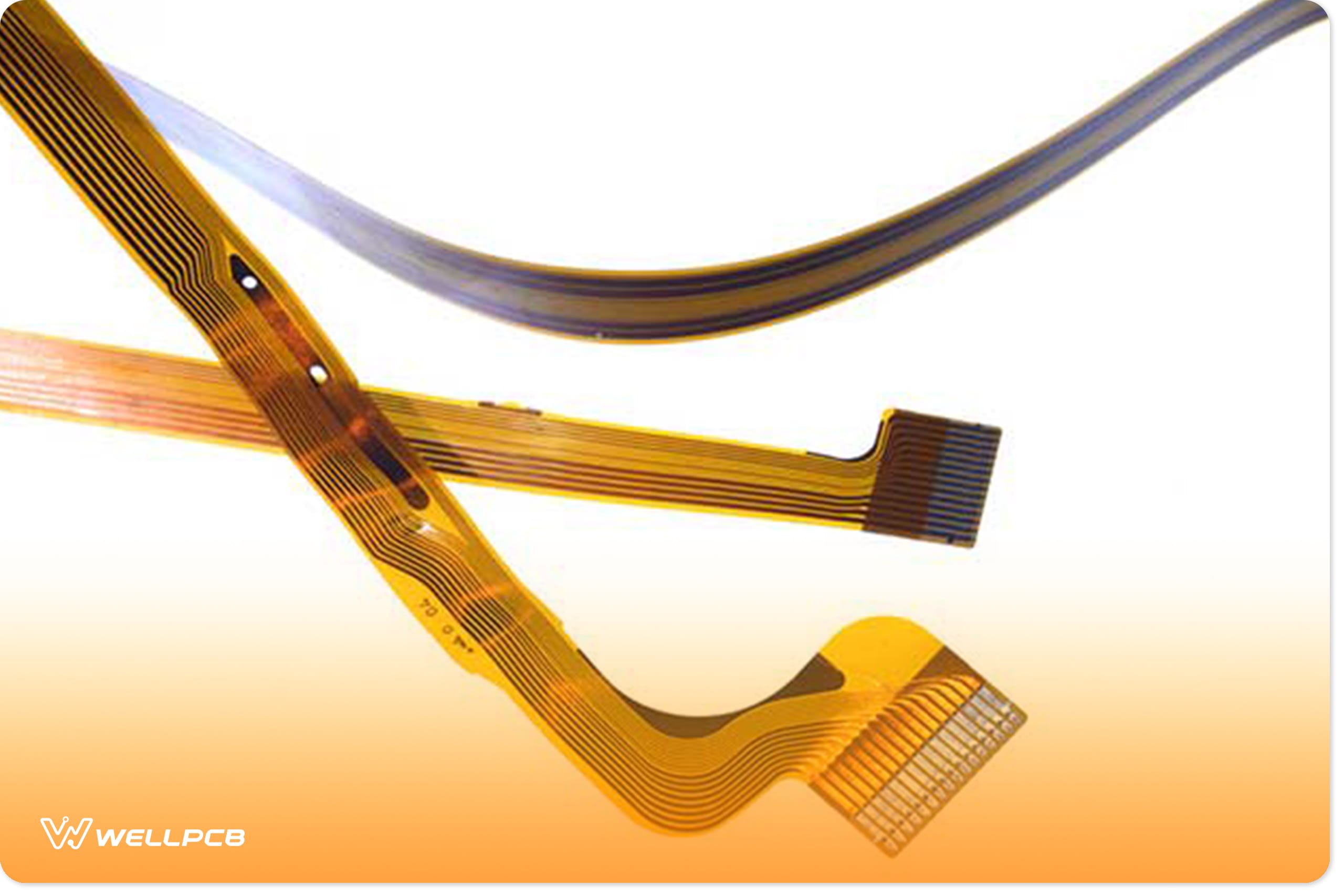
Flexible Flat Cable – How to Make your Designs More Innovative?
Do you want to make electrical connections in a lightweight, small, and flexible package? You can easily do so using flexible flat cables. Flexible Fl...
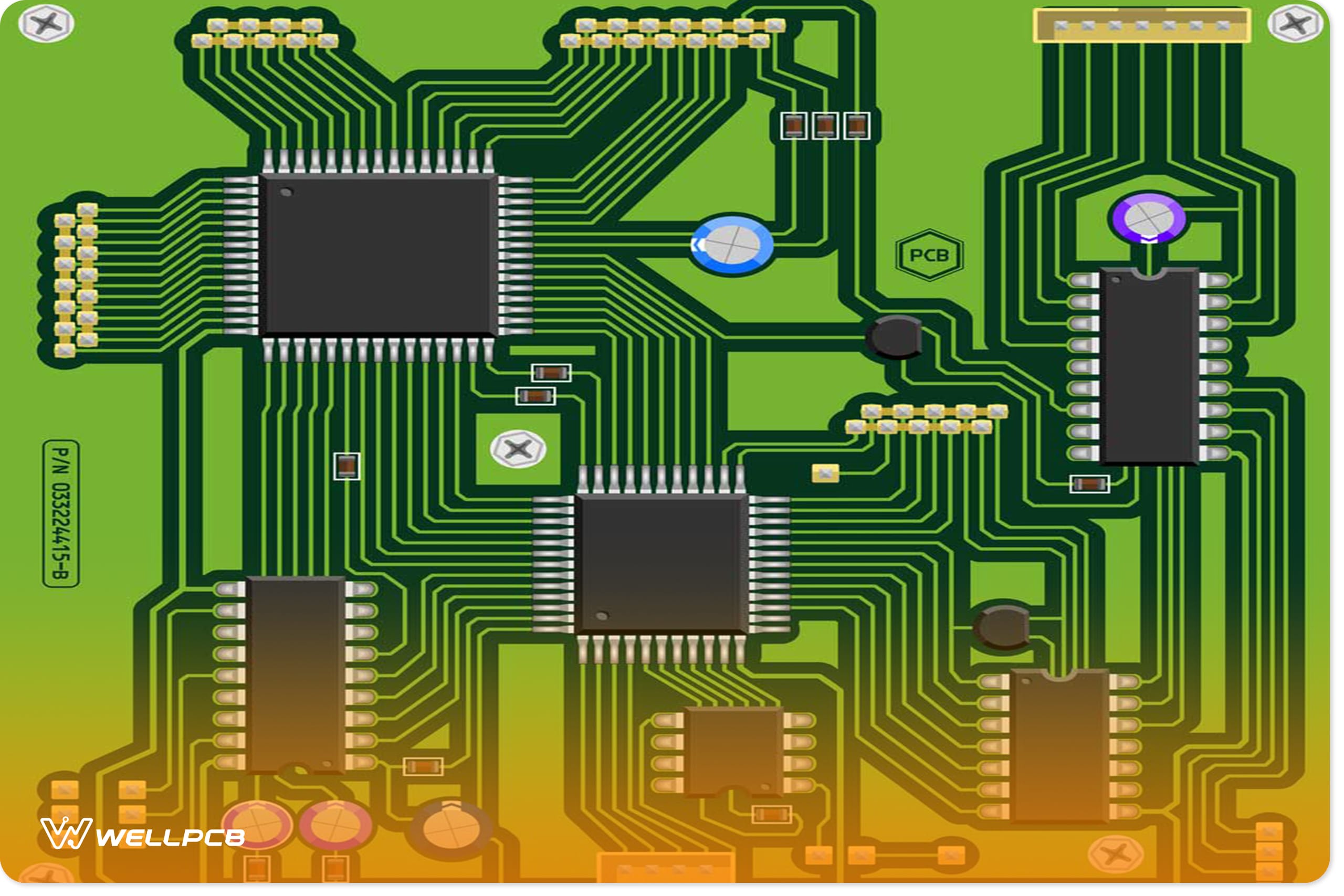
Edge Connector Beveling-Gold Finger Plating for Edge Connectors
Edge Connector Beveling We live in a mobile-activated and digital world where signals are sent and received between several devices. Effective communi...
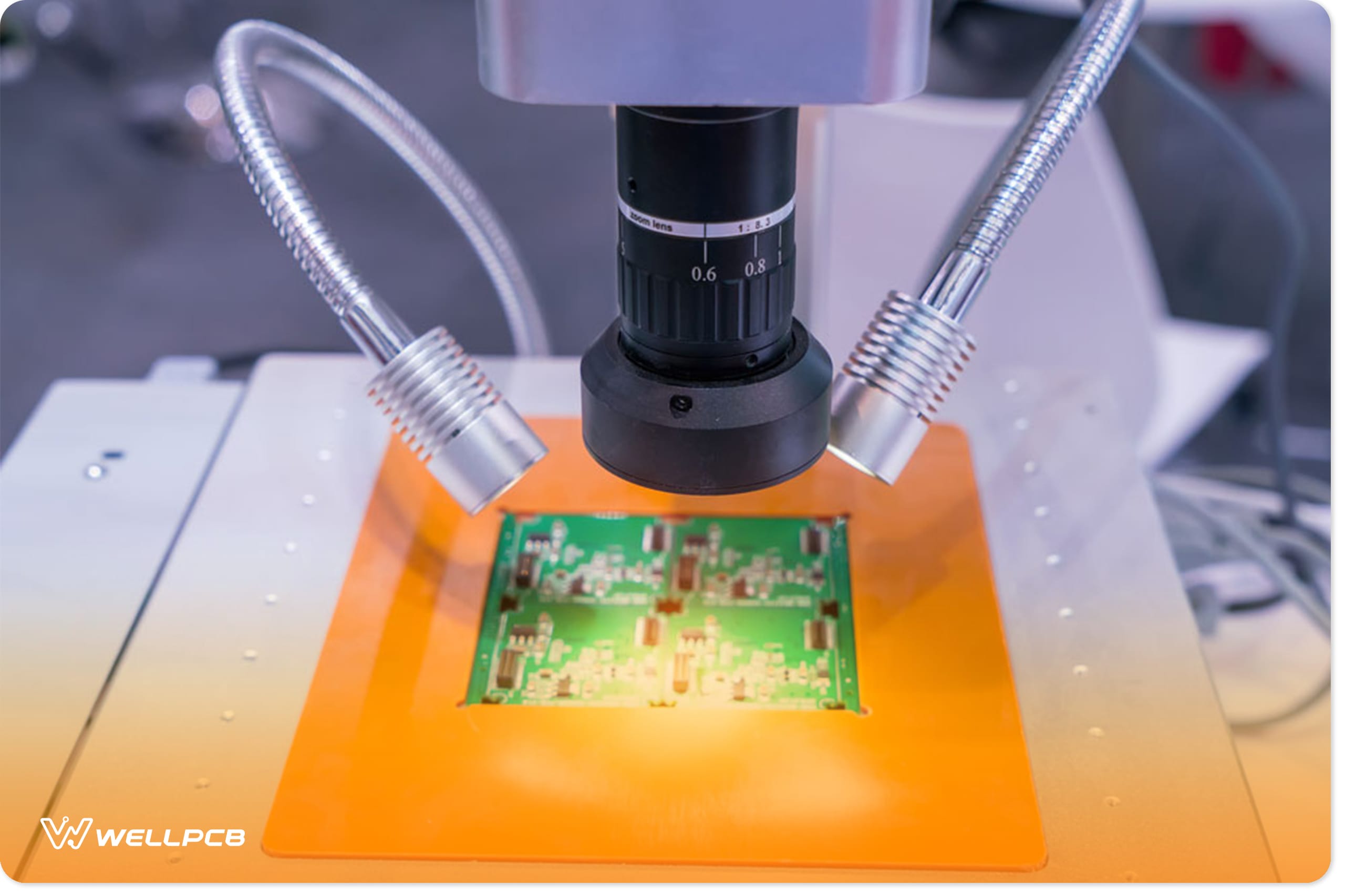
Presensitized PCB: An Ultimate Guide
Printed circuit boards (PCBs) are the backbone of every electronic device. Understanding how they function and work is paramount to PCB manufacturing ...
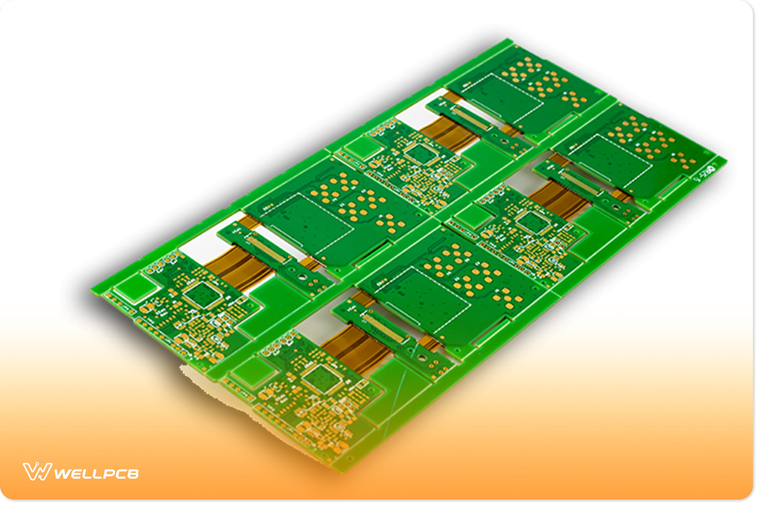
Rigid-Flex PCB-How to Streamline and Improve Reliability
Rigid-flex PCB and flexible printed circuit boards are becoming more popular every day.
If you would like to discover more about streamlining assemb...

Standard PCB Drill Sizes-Tips You Should Know
A few decades ago, PCBs were drilled using simple drills. Typically, the operator had to move panels to the relevant Y and X coordinates and pull the ...
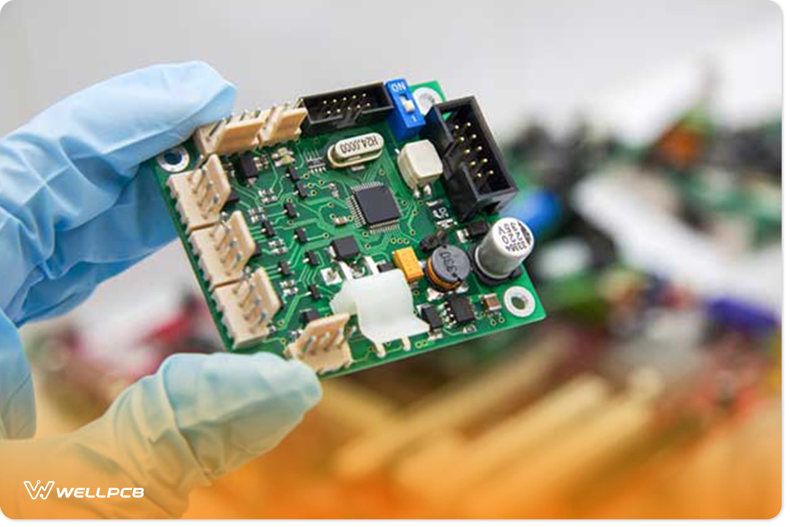
Low Volume PCB Assembly Process Ultimate Guide
There are times when you need printed circuit boards for your application, but you don’t need a large number of them. The solution lies in the low vol...
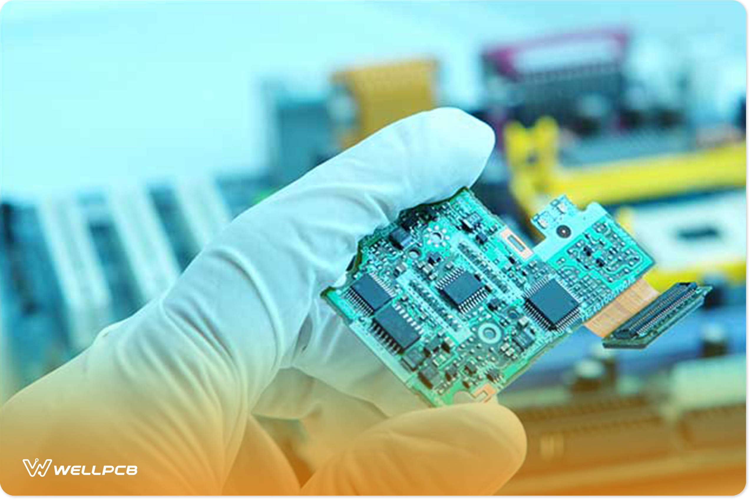
10 Awesome Advantages of Rapid PCB Prototyping Service
Without a proper plan, implementing new PCB products can introduce further unnecessary delays and expenses. Rapid PCB prototyping is a useful practice...

Ultimate Guide to PCB Design and Manufacturing
PCBs are no longer new, but their importance in electronics cannot be overstated because they make it possible to organize large circuits and componen...

PCB File-How To Make Your Files High Availability
As a student, you often don’t know how to deal with different PCB files. As an engineer or designer, you may need to mass-produce printed circuit boar...
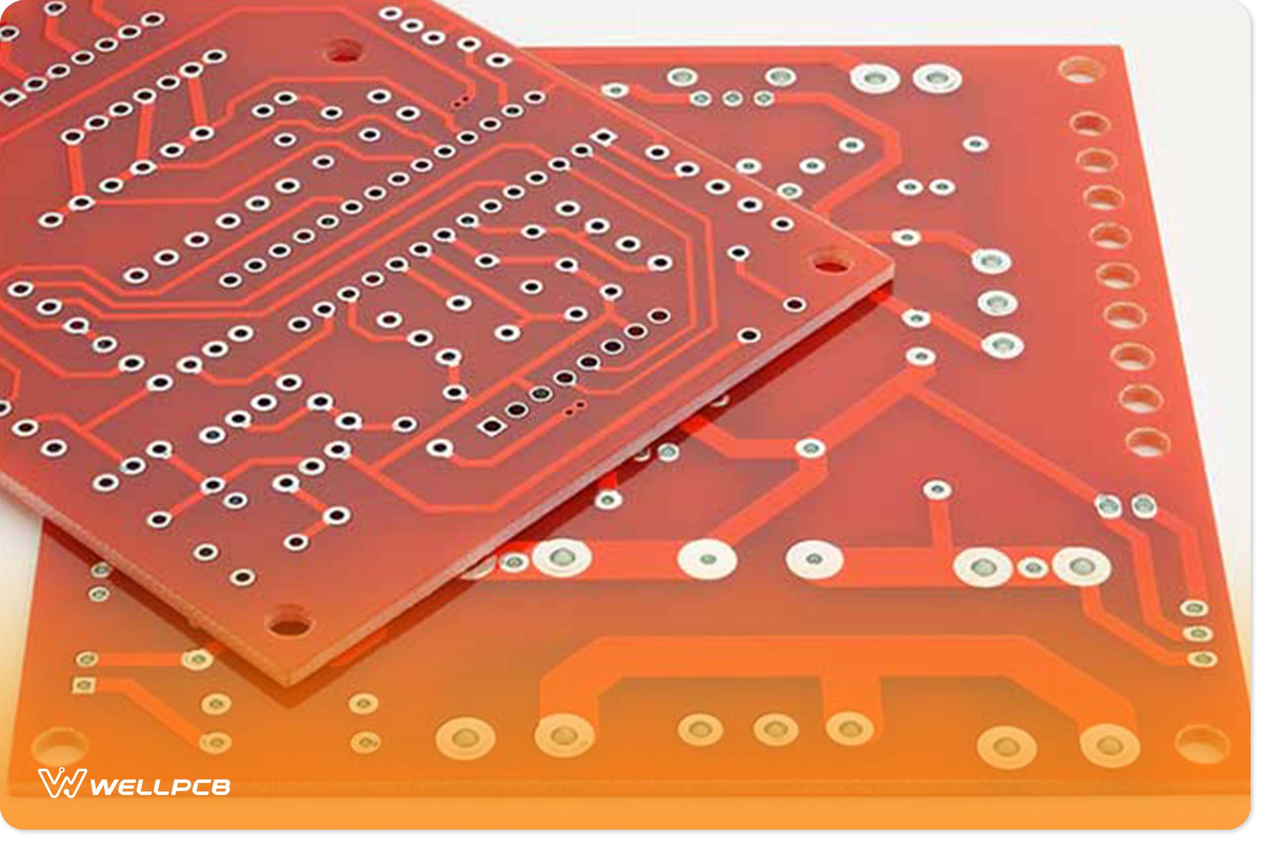
Single-Sided PCB – The Ultimate Guide to How to Save More
What is a single-sided PCB, and how can they be used to enhancing electronics?
Many have asked this question, and more and more evidence exists that ...
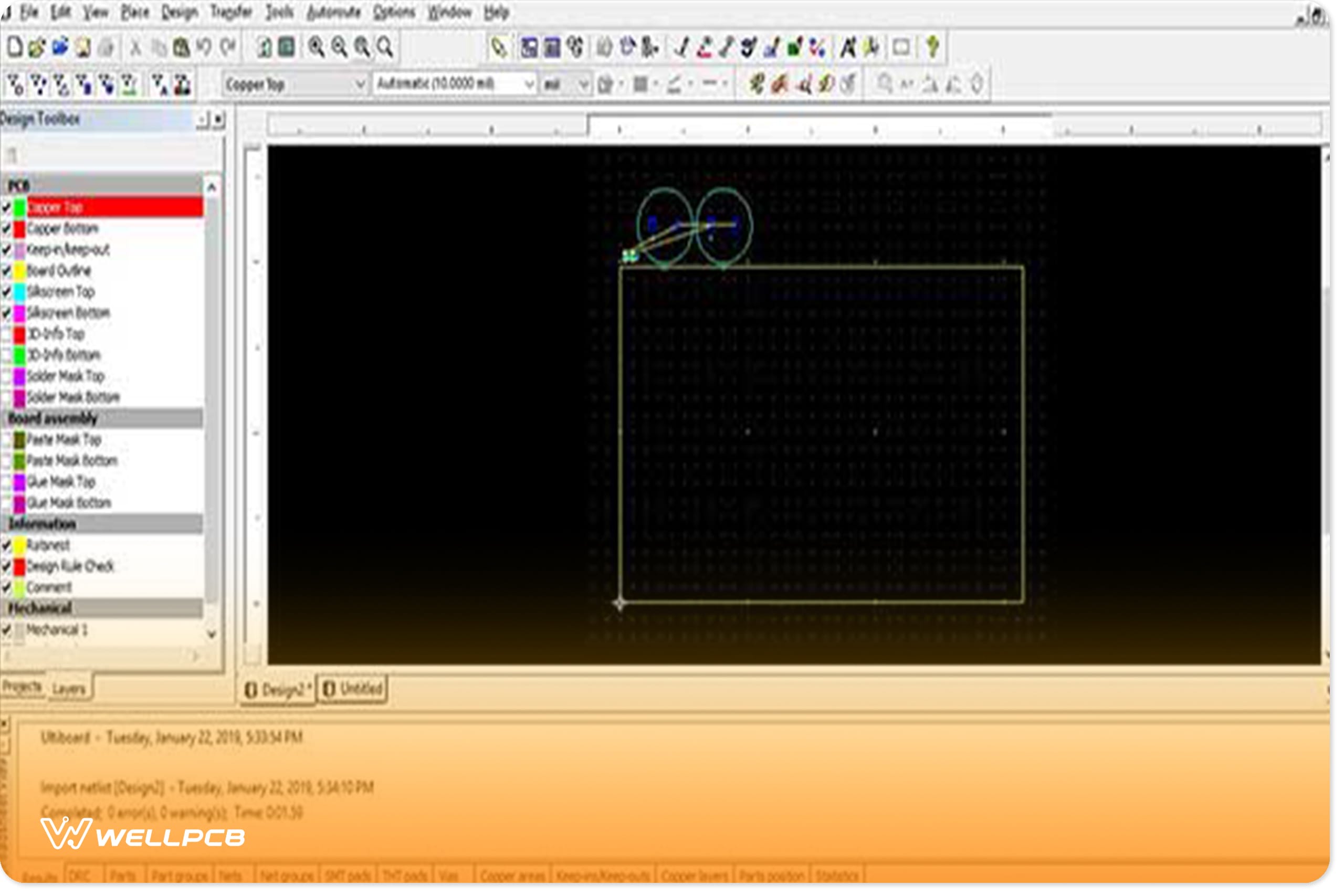
Ultiboard – The Ultimate Guide For Best For Beginners
Electronic circuits have been around for a long time now, and like any design, modeling is essential for manufacturing the end product. PCB layouts an...
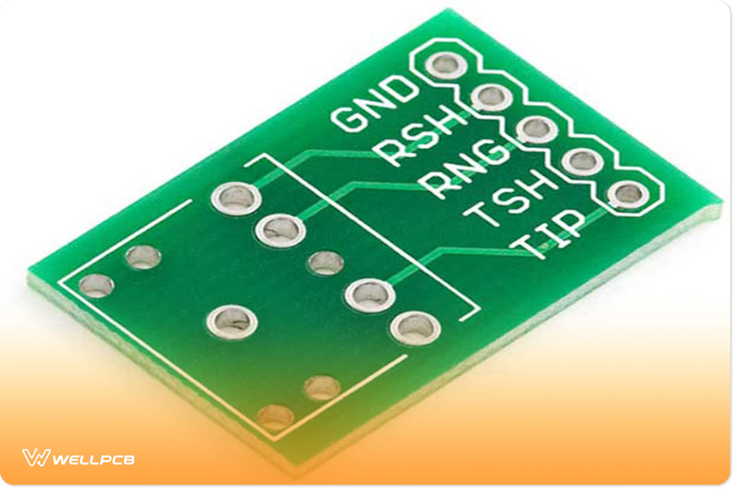
Bare PCB-Simply Know About It’s Technology
As the name suggests, bare PCB is created so that you can configure and populate them with components depending on your needs.
It is the engineers' j...

10 Tips for Choosing the Right PCB Manufacturer and Supplier in China
Today’s electronic devices and computers being used are helpless without a printed circuit board. You will find many PCB manufacturers with profession...
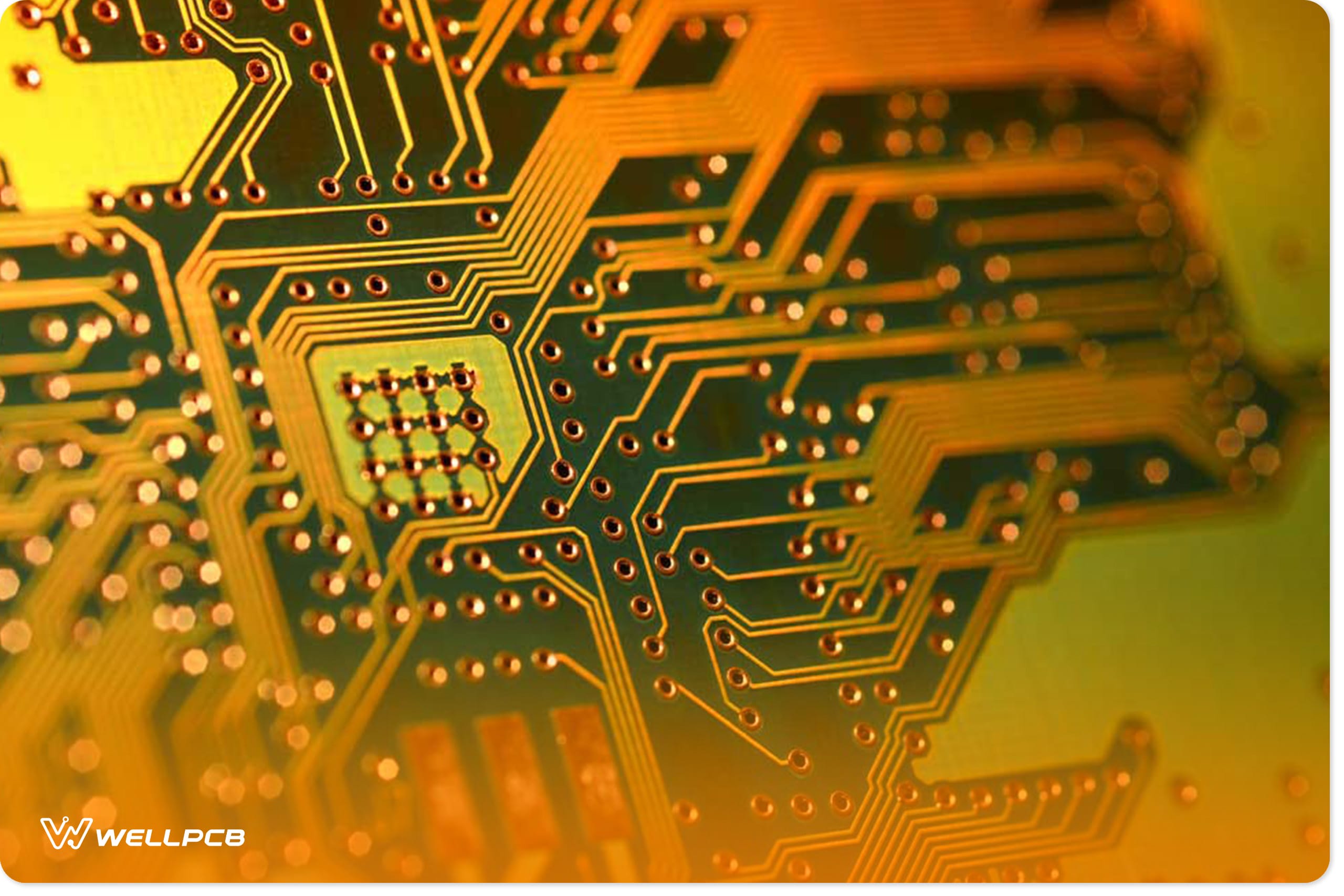
PCB Stencils-The Ultimate Guide On How To Make It
The printing phase is the most critical part of a PCB assembly. It's also the diciest, as the slightest error can ruin the finished PCB electronic. So...

NRE Cost – How To Make the Project Perfect
Projects involving printed circuit boards (PCBs) are not cheap and do not require a short time to complete. Successful start and completion of any giv...
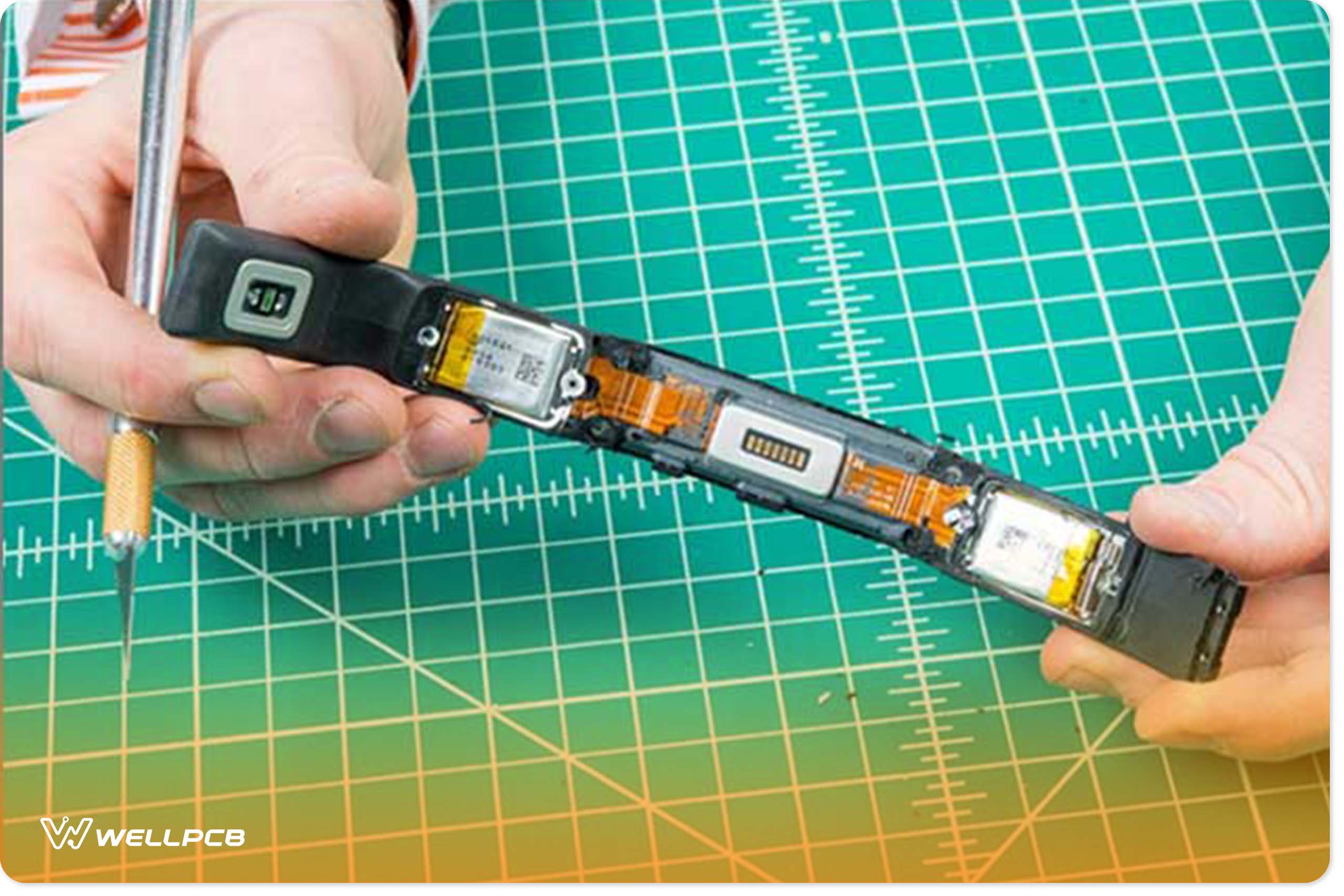
FPC Electronic-All There is to Know About Flexible Electronics
You’re probably used to seeing the internal components of a computer comprised of rigid, rectilinear circuit boards. But FPC electronics is a paradigm...
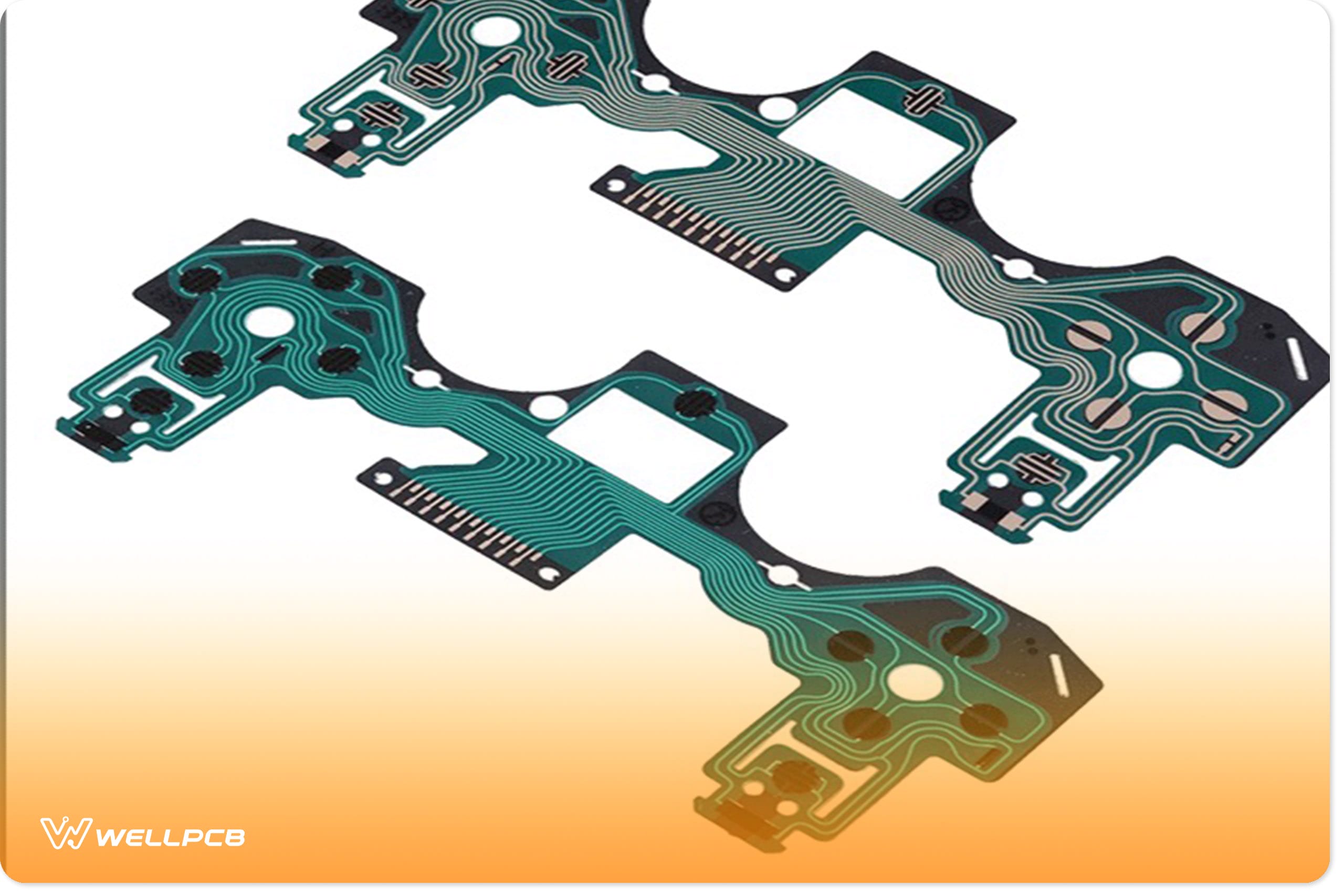
PS4 Controller PCB Circuit Board – What You Need to Know
Just a short while ago, my PS4 Controller suddenly failed.
The D-pad directions stopped working on my PS4 Controller, but the Controller was in other...
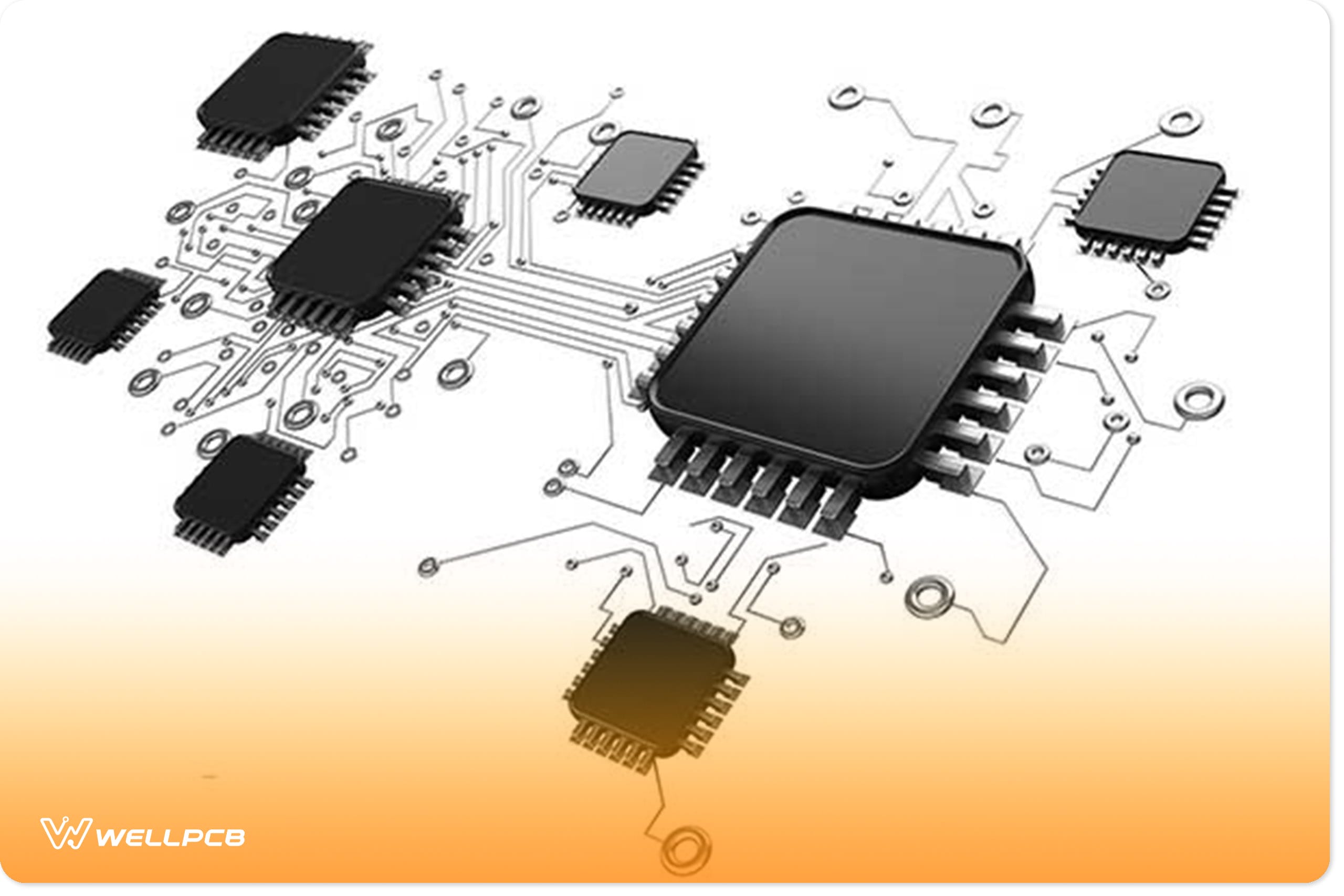
Sprint-Layout – The Ultimate Tutorial And Experience
Sprint-Layout is a software tool used to design single-sided, double-sided, and even multilayer printed circuit boards (PCB). The software aims to bet...
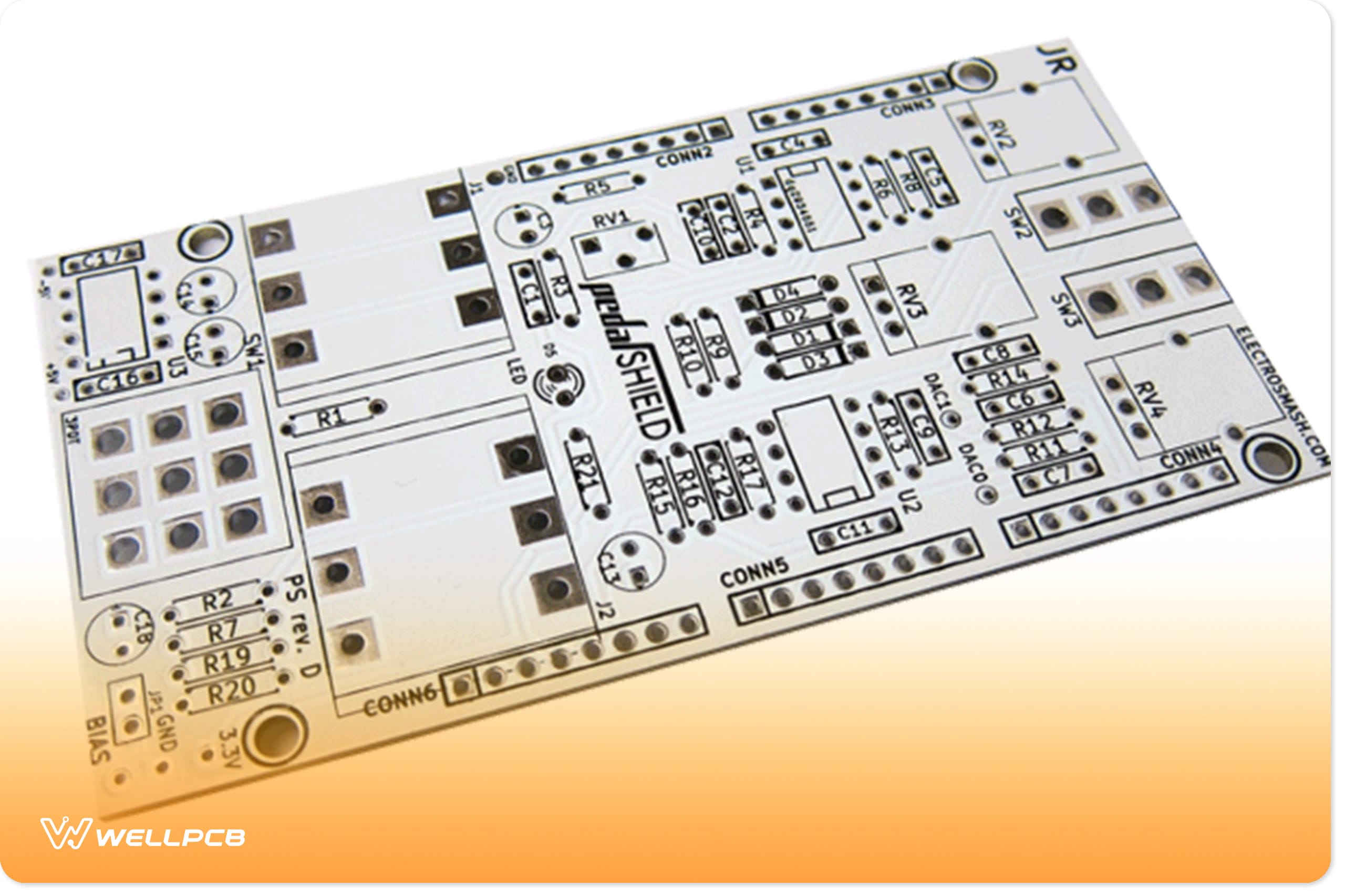
White PCB – An In-Depth Guide About It
I have a question for you, what’s the color you most see on a PCB? If your answer is green, you would be correct, but that answer leads to another que...
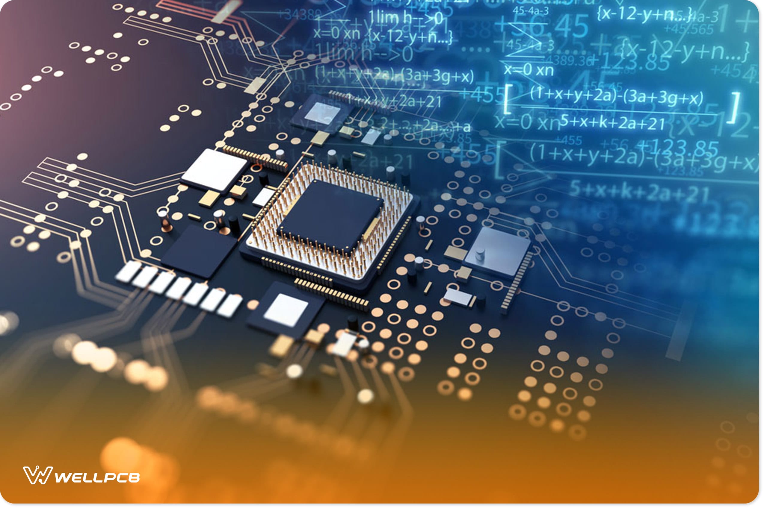
94V-0 Circuit Board – The Ultimate Guide Is Here
In a nutshell, the 94V-0 Circuit board is defined as circuits inscribed on PCBs (Printed Circuit Boards) that have met the UL 94V-0 flammability test....
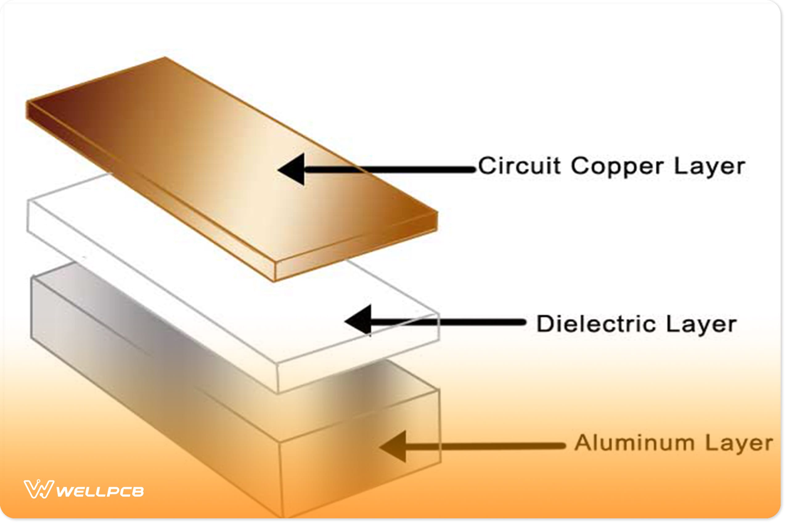
PCB Material-(Selection requirement while designing the PCB)
In PCB manufacturing, you need to consider how to choose the right material for your PCB design.
There are many different types of materials, each wi...
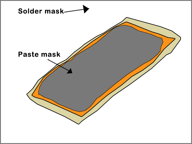
Solder Mask – The Most Comprehensive Introduction Is Here
After a printed circuit board manufacturing, the copper traces on the substrate are usually at risk of oxidation and rust due to environmental exposur...
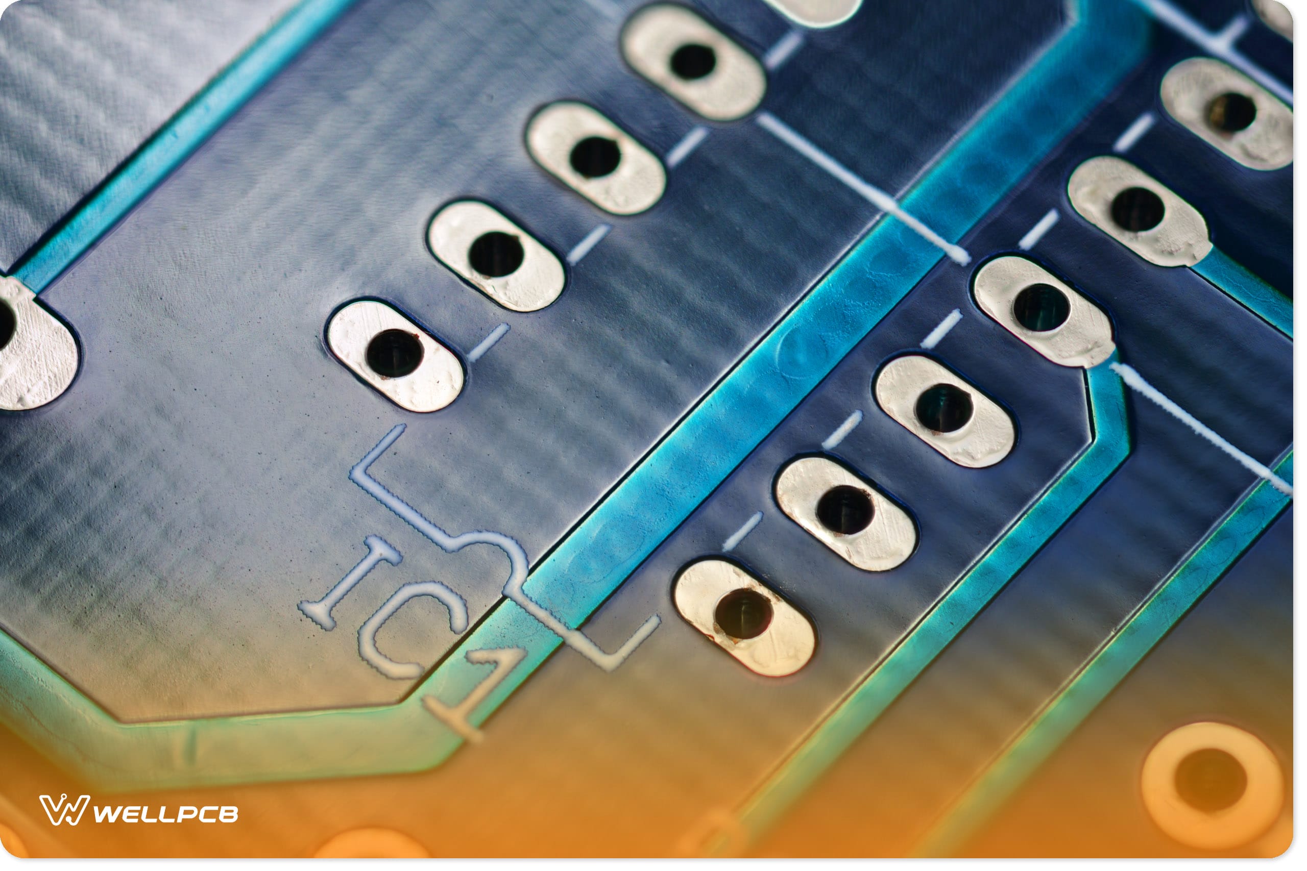
A Guide to Moving from Breadboard PCB Prototypes to Full Product
Scaling from breadboard PCB prototypes is a complicated process that combines creativity and procedures.
The timeline for development is as indivi...

PCB Trace Thickness: What You Should Know
PCB boards are the backbone of modern electrical and electronic devices, and their importance cannot be overstated. Trace thickness is a critical desi...

How to Repair Circuit Board
The world comprises thousands of Printed Circuit Board industries distributed in different regions across the globe. These are industries majorly invo...
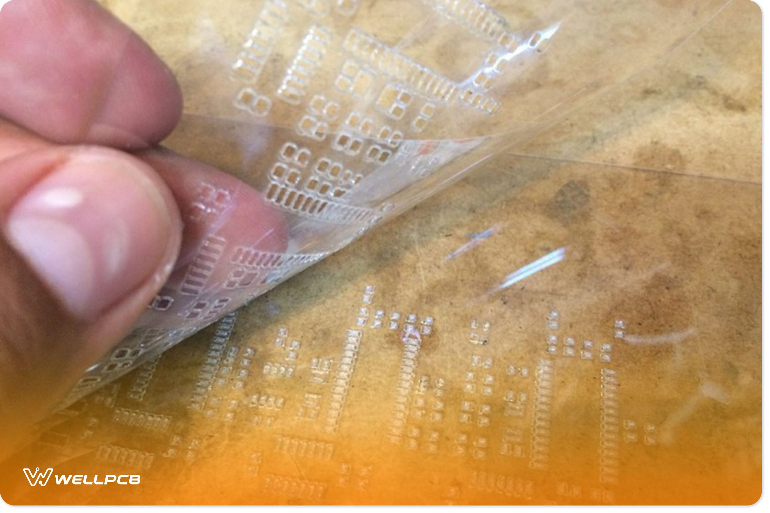
Mylar Boards-How To Do With It
When you consider the challenges of working with surface mount segments, the main thing that frequently strikes to mind is endeavoring to solder those...
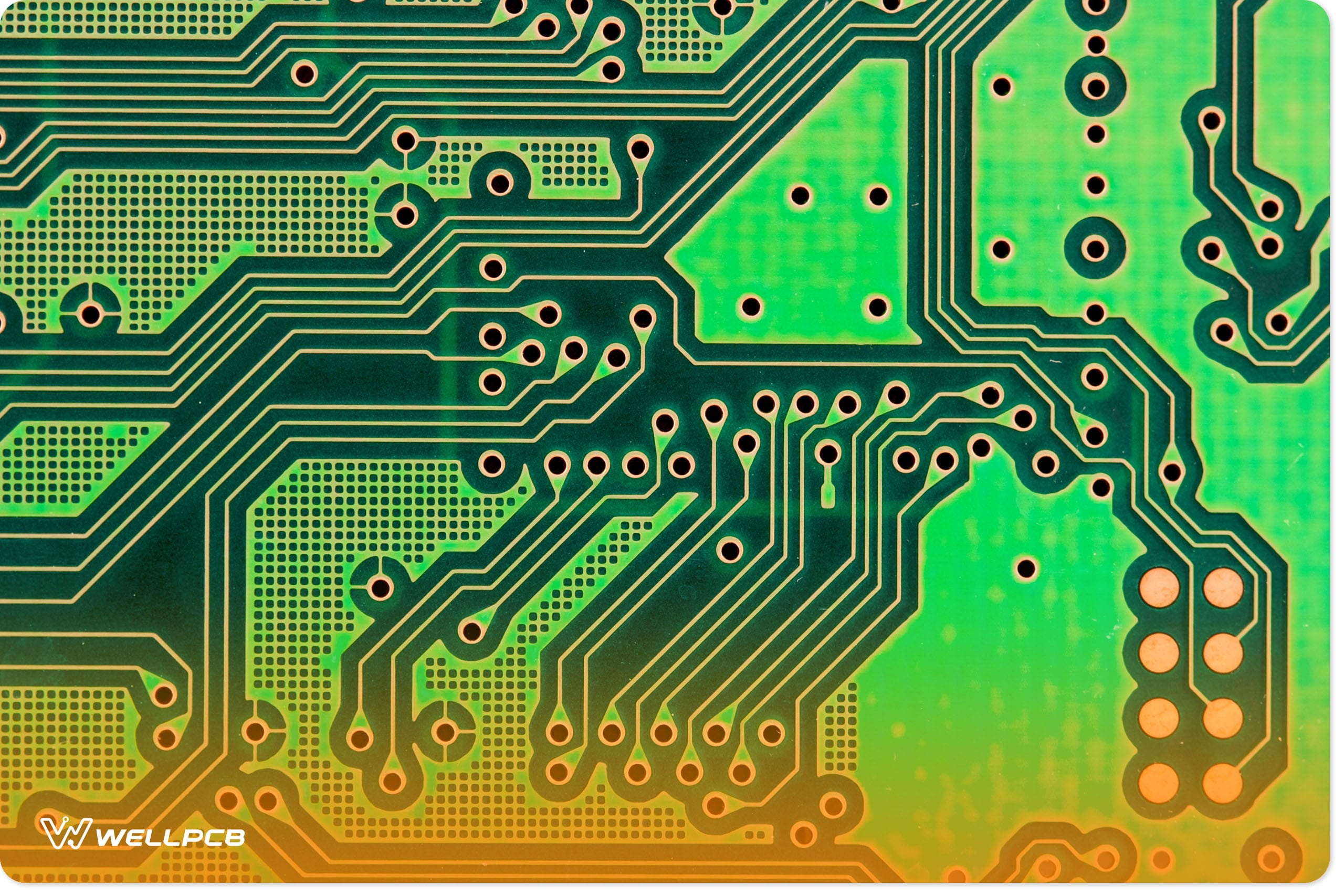
PC Boards-Manufacturing Tips Ultimate Guide
Working with Circuit boards can be exciting, especially for an experienced technician. Unfortunately, if you are inexperienced, you may find soldierin...
Kicad Tutorial-Simple And Valuable Fundamentals
This tutorial takes you through how you can use Kicad Tutorial in creating, editing, and library linking of PCBs before they are exported to gerbers f...

PCB Manufacturing Equipment-Important And Valuable
To manufacture printed circuit boards, one requires an assortment of equipment, including a hydraulic vacuum press system, strippers, etchers, cleaner...