


Contents
- 1 Draw the Schematic of your Custom PCB
- 2 Find Software for Designing the PCB Layout
- 3 Decide the Type of your PCB Package
- 4 Define your Design Specifications and Place Components
- 5 Route your Circuit Connections
- 6 Check the Final Layout of Your Custom PCB for Design Errors
- 7 Decide the PCB Materials that You Want to Use
- 8 Arrange your Custom PCB Files
- 9 Find an Online PCB Manufacturer to Order Custom PCB
- 10 Summary
Draw the Schematic of your Custom PCB
Before you begin wiring your electronics project, you need a circuit diagram for reference. It is not the best practice to blindly start putting together the components. In the same way, you need a proper circuit diagram before you can start making the custom manufacturing of PCBs, there are high chances of layout failures, which can go a long way into negatively affecting the final product’s functionality. There are several PCB layout. For inspection, you may begin with an already designed circuit available on the internet, or you can build your own from scratch.
Wee recommend that you start with a simple project. It can be something as simple as a blinking LED. Now let’s discuss the ways you can capture the circuit schematics of your project. There are many custom PCB design suites available online which offer schematic capture tools. You can enter your circuit diagram into it or get help from other external packages.
Moreover, you can also perform simulations of the circuit diagram to make sure that your custom PCB will work. Finally, you will have files containing the schematics that can transform into a netlist. The netlist has all the information regarding interconnectivity between circuit nodes, component pins, and nets.

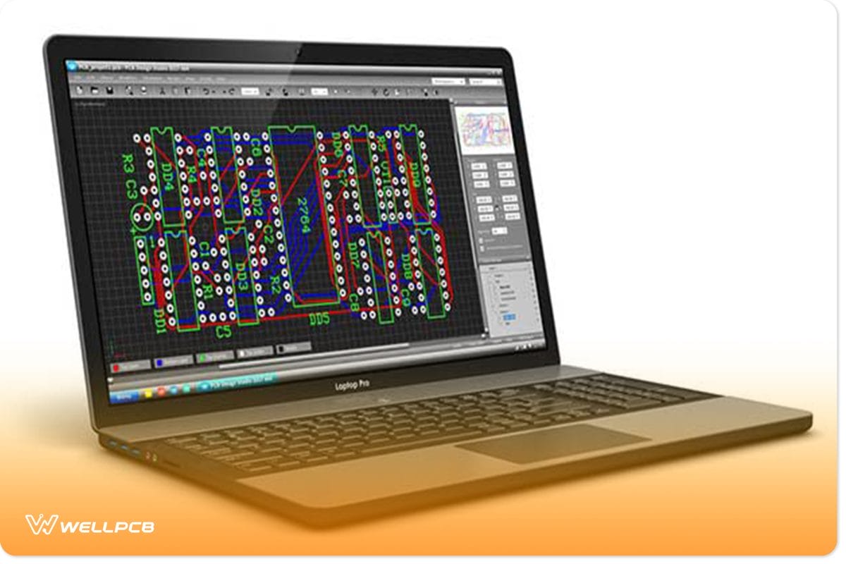
Find Software for Designing the PCB Layout
The next step is to draw the custom-printed circuit board. You are required to turn the schematic diagram into a design for a custom PCB. Therefore, all you need is software for designing the layout. It is not at all hard, no matter how complex it sounds. It’s the software’s job to compare the schematics file with your drawing. It will also assist in making the same electrical connectivity. You can use custom PCB design software such as Altium Designer, Eagle, Proteus, KiCad, and similar.
If you need to design a PCB layout, you can learn. However, we do not recommend that you learn to operate the software from scratch because it will waste a lot of time, and there will be many mistakes. You can find a PCB design engineer and tell him what you think. For a professional PCB engineer, it is easy to draw the PCB layout you need using computer software. This saves you time and effort. You can spend more time with PCB suppliers.
Decide the Type of your PCB Package
Furthermore, you also need to know how you are going to arrange the components on the custom PCB. There are two ways in which the electronic components attach to the printed circuit board:
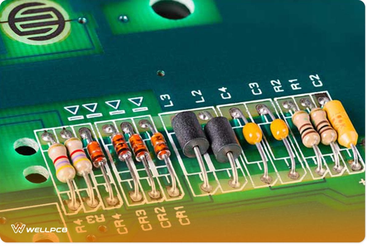
1. Through-hole: In this way, the electronic components with leads attach to the custom PCB via holes. You will need to define it in the software when you are setting the specifications of your custom PCB layout.
We can optimize our design by comparing the direct advantages and disadvantages of through-holes and non-through-holes to make your design easier and avoid making mistakes.
| Advantage | Disadvantage |
| Simplify prototyping and testing | Requires more expensive drilling |
| Relatively cheap | Take up more space on the board |
| High heat resistance | The assembly process involves more |
| Strong physical bond | Slower speed |
| The high power processing capability |
|
2. Surface mount: With the advent of technology, surface mounting is the preferred method for applications requiring small and low-cost PCBs. You can mount such electronic components directly over the surface of the custom PCB without boring any holes.
Define your Design Specifications and Place Components
Now, you need to have a rough idea of the locations of the components and if the custom PCB has enough space. These details will allow you to make decisions related to the required number of layers and board size. Then, you can proceed with creating a more detailed custom PCB layout. More details can include data such as devices’ proximity for communication purposes. If you are using any RF devices, you can add related information.
Keep in mind that all the components’ data need to be defined before you can identify them in the custom PCB design. You may need to tell any drilling info, areas to be avoided, and their footprints. Also, many components may have similar fingerprints, so you don’t need to define them every time. Furthermore, the PCB design software also has libraries of parts and will save the new information for the future.
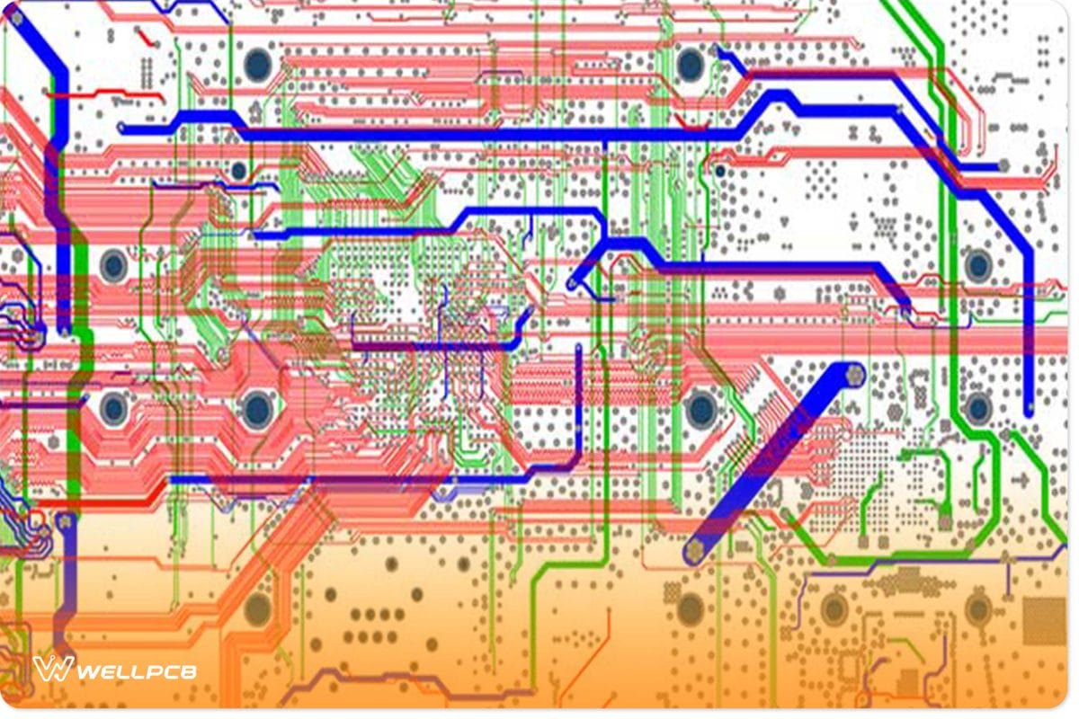
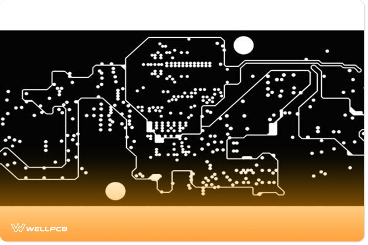
Route your Circuit Connections
Now, it’s time to route the circuit connections after you have placed all the components. You can route manually or select the Autoroute option in the design software. If you choose auto-routing, the software will pick the netlist of the circuit schematics and then direct the physical connections accordingly.
Custom PCB signal integrity evaluation must be done during PCB design because rectification may be difficult after manufacturing. Use reliable PCB design software will take the no. of layers data to create via holes. Also, one layer is mostly for power and another for a ground connection. However, auto-routing can take a lot of computing power if the PCB design contains thousands of components. So, you need to stay put in that case as routing may take time.
Check the Final Layout of Your Custom PCB for Design Errors
Almost all the PCB design software comes with a design rule checker. It is usually only termed as DRC. After routing, you may verify your PCB design layout by running this feature. In general, there are lots of rule types, so you may only select the ones that you need. It is not compulsory to check the design for every rule.
You will need to select or deselect any rule that is not required individually. If you are using Altium Designer, you will find rules in the PCB Rules and Constraints Editor. You can also define new design rules. Furthermore, you should make sure that the rules you are following are according to the tolerances and specifications of your custom PCB manufacturer.

Decide the PCB Materials that You Want to Use
The PCB material that you decide must fulfill the requirements of the custom PCB design. It also may take into account the PCB cost and product quality. With design requirements, we meant the institutional and electrical parts. If you are going to design a PCB for high-speed applications, then the right material decision is critical.
If the frequency is in GHz or more, then it may not be wise to use the commonly used FR-4 PCB material. Because the dielectric loss at these frequencies can cause attenuation of the signal. The following are some of the PCB materials that you may choose from:
Conductor Material:
- Rolled copper foil
- Electro-deposited copper foil
Substrate Material:
- Polyimide
- Polyester (PET)
Epoxy imprinted fiberglass
- Adhesives Material:
- Acrylic
- Epoxies
- Polyimide
- Polyester

Arrange your Custom PCB Files
Finally, you need to generate PCB files of your completed custom PCB design layout. These files should have all the necessary information and data to manufacture your PCB. The custom PCB manufacturer also needs to know if there are any special requirements. It will be only then that they will be able to produce PCBs precisely the way you want.
Generally, most custom PCB manufacturers accept the Gerber file format. The same file format that you will get after saving your PCB design files. The software generates them automatically. In addition to these files, it also produces a file containing the drill information.
Drilling is one major factor that affects the cost of a custom PCB. We know that a few designs may need extra drilling, as there is a requirement for some holes for fixing traditional components. But, if you want to reduce your costs, we would recommend you do you use a smaller number of holes. It will also save you time.
Find an Online PCB Manufacturer to Order Custom PCB
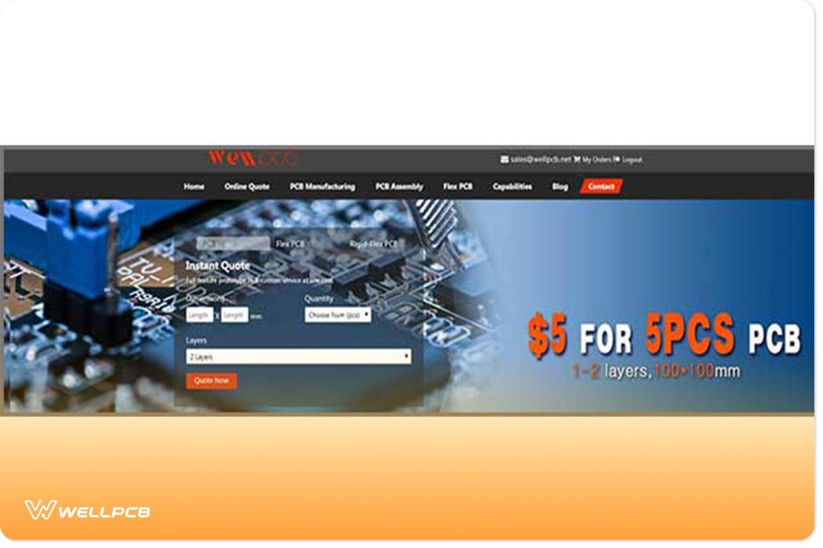
Now, the question is what to do with these files? You are now required to find an online PCB manufacturer that meets your needs. And how can you make sure of that? The easiest way is to read customer reviews related to them online and give them a chance.
Once you have selected an online custom PCB manufacturer, go to their website and look for “Place an order.” There, you will need to upload the Gerber files and fill in any other required information. This is it! You are ready to order your first custom PCB.
Summary
We here at WellPCB also take online orders and can manufacture your custom PCB layouts. If you need any help, merely contact us today, and we will assist you straight away. We also provide an online quote service; you only need to upload the custom PCB design files and provide the information. We will then estimate the cost of your custom PCB production.


