Contents
- 1 What is a Back Drill PCB?
- 2 Why is Back Drilling Required?
- 3 Advantages of Back Drilling
- 4 Complexities of the Back-Drilling Process
- 5 How much Leftover Stub Length Can You Have?
- 6 How Much is Drilled?
- 7 Backdrill Vs. Blind Via
- 8 Applications that Use Back Drilling
- 9 Challenges of Back Drilling Process
- 10 Factors Influencing Back Drilling Effectiveness
- 11 FAQs
- 12 Final Words
What is a Back Drill PCB?

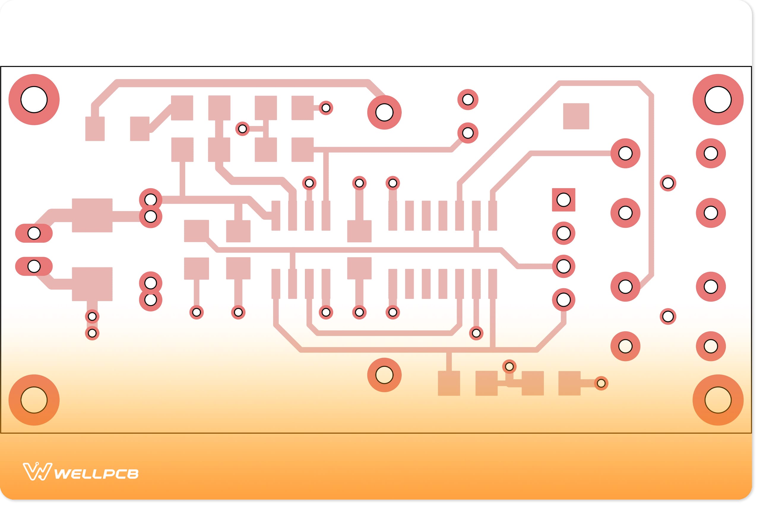
Multiple printed circuit boards
The sad truth about high-speed PCB designs is the sheer amount of problems they have. No doubt, maintaining signal integrity tops the list of concerns.
But it’s easy to solve with proper design and manufacturing practices.
Interestingly, Vias have a non-functional section called the Via stub. Sadly, this part causes annoying signal integrity problems in high-speed PCBs.
And the stub end can create signal reflections that interfere with the board. Thankfully, you can counter this with back drilling.
In truth, the process involves re-drilling a slightly larger hole than the PTH to remove the via stub. So, back-drilled holes reduce the stub’s length to about ten mils.
Note: Stubs more than ten mils will produce signal reflections.
Why is Back Drilling Required?
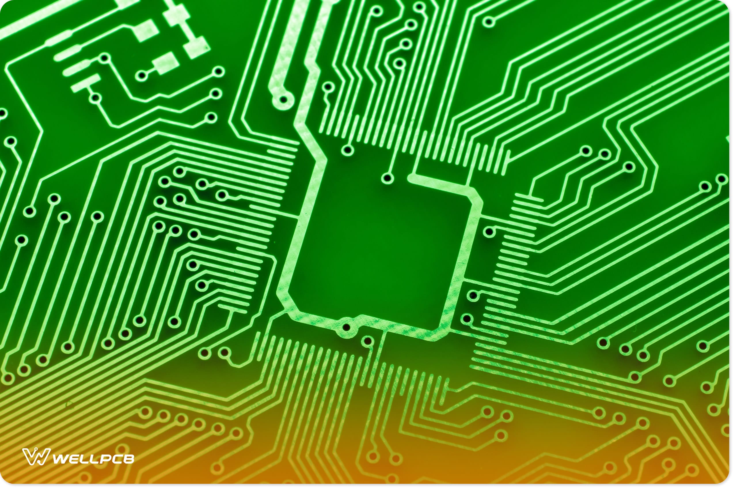
PCB drilling
Back drilling is necessary for shortening the via stub. Usually, this unused portion of the via’s copper barrel won’t contribute to the PCB’s design and will only interfere with high-speed signals.
Typically, back drilling results in a Via stub lower than ten mils, crippling the copper barrel’s ability to create signal reflections.
For example, you have a through-hole Via drilled from layers one to ten in a 10-layer stack-up.
And your designs require signals in layers one to three; the via will have a stub after the third layer. Unfortunately, this unused portion creates high-frequency reflections and resonance.
Therefore, you’ll need back-drilling to remove the extra copper plating after the third layer.
Also, your back drill must be larger than the PTH’s original size. Otherwise, you won’t remove all the unwanted copper.
Advantages of Back Drilling
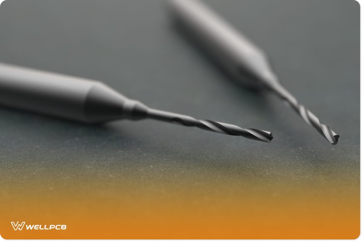
PCB drill bits
Here are the benefits of using back drilling on your PCBs:
- Back drilling dampens signal attenuation. And the process reduces the stub’s enhanced impedance matching while mitigating its EMI/EMC radiation.
- You can also avoid signal distortion issues with back drilling. Via stubs are notorious for causing deterministic jitter and are the results of signal crosstalk, EMI, and noise.
- Back drilling reduces via-to-via crosstalk.
- Reducing deterministic jitter with back drilling lessens your signal’s overall BER (Bit Error Rate).
- Diminished excitation of resonance modes.
Complexities of the Back-Drilling Process

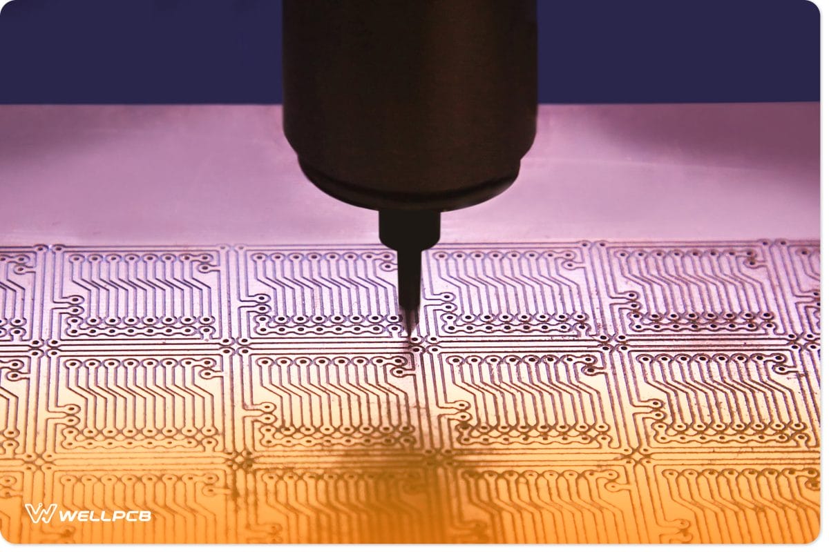
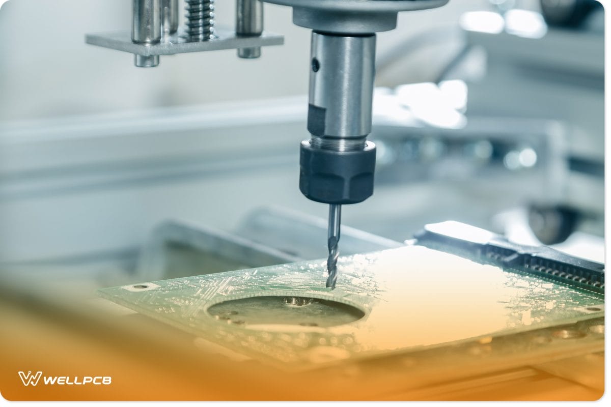
Machine drilling PCB
Here are some areas you may find tricky while using the back-drilling process:
Back Drilling Depth Control
Many things could go wrong with back drilling. For instance, if the back drilling machine is inaccurate, you may have low via tolerance. Hence, it’s crucial to control your back drill depth.
Further, several ‘outside’ factors may affect your back drilling depth.
For example, you may have drill resistance, drill tip angle, effective contact between the cover board & the measuring unit, and board warpage.
Hence, you must choose suitable drilling methods and materials during production. So, you should get higher depth control for more accurate results.
Back Drilling Accuracy Control
As mentioned earlier, accuracy is critical for back drilling. So, your preferred drilling method, board contraction & expansion, and equipment precision can affect the overall back-drilling accuracy.
How much Leftover Stub Length Can You Have?
Drill working on a PCB.
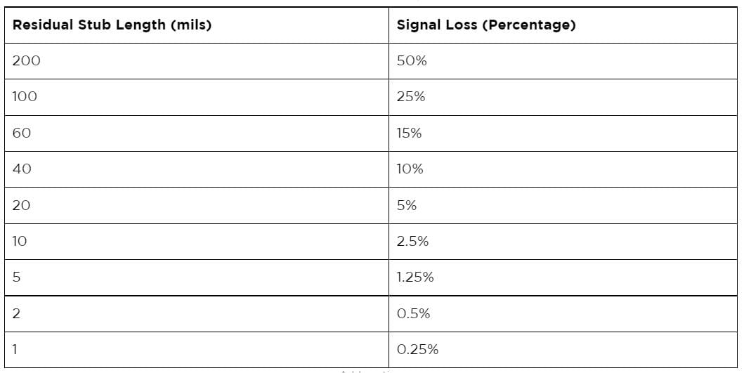
When back drilling, you must figure out how much residual stub length won’t affect your PCB.
However, deciding this factor depends on several considerations, including your preferred signal integrity and practical manufacturing processes.
Typically, decreasing the maximum leftover stub length and increasing the Vias for back-drilling will fuel manufacturing costs.
Here is a table showing the leftover stub length and corresponding signal loss.
How Much is Drilled?
Although there’s no predefined amount, there are some hard-set parameters that guide back drilling to get better signal quality.
For example, the ideal diameter to ensure a clean removal of the stub is about 4-6 mills larger than the via’s diameter.
Remember, you must leave only less than 10 mils of the remnant via stub.
Any more than 10 mills will compromise signal reflections. You could lose as much as 20% of the signal if the residual stub length is 100 mils.
The amount drilled can affect the PCB price. The back-drilling PCB cost can inflate the overall board price by about 20%.
Backdrill Vs. Blind Via
Clearly, a backdrill and blind via are different things in a PCB.
While a back drill is more of a procedure, a blind via is a pathway in a PCB that connects the inner and outer layers. Unlike a back drill, a blind via doesn’t have a visible open-ended exit in a PCB.
You can differentiate a blind vs. back drill using these characteristics.
| Blind Via | Back drill |
| The primary purpose is to utilize surface space in the least destructive way possible to the top or bottom PCB layers. | The primary purpose is to reduce signal reflections by removing via stubs. |
| You’ll most likely find them in PCBs that need compact designs and dense layers. | You’ll likely find back drills in designs that need high-frequency signals with minimal reflections. |
Applications that Use Back Drilling
PCB board showing layers
Controlled depth drilling PCBs(back drilling) are responsible for the success of many everyday operations in small-scale and industrial-scale electrical items.
Multi-gigabit data channels and high-frequency RF Microwave circuit boards have one thing in common besides using back drilling.
They rely on high speed and high frequency that need minimal signal loss.
In computing, you will find instances of back drilling in DDR3 & DDR4 memory routing and servers & network switches.
In communication systems, back drilling plays a crucial role in fiber optic transceivers and telecommunication infrastructure that need to maintain signal strength.
High-Density Interconnect PCBs (HDI PCBs) are in medical, IoT, and automotive devices.
HDI PCBs require absolute signal precision and minimal loss. Therefore, back drilling is a key part of their manufacturing.
Most consumer electronics have multiple layers. And with such stacking, it is normal to have via stubs.
Therefore, back drilling becomes an integral part of the manufacturing of consumer electronics PCBs.
Challenges of Back Drilling Process
Back drilling is a sensitive procedure. Inaccuracies can render an entire batch of boards unusable. The procedure faces two major issues that affect quality.
Accuracy Control

Precision measurement in PCB testing
Given the precision needed for optimal PCB performance, accuracy is a big concern during back drilling.
You’ll need accurate drills, precise measurements and pinpoint procedures to ensure any dimension changes don’t affect board function.
Board expansion and contraction caused by inaccurate tools and processes during back drilling will compromise signal strength and EMI sensitivity.
Back Drilling Depth Control
Depth control will affect the outcome of the back-drilling process. Here, drilling equipment, the number of layers, and the accuracy of measurements influence signal transmission.
Other factors related to back drilling include the drilling angle and board thickness. These factors present a major quality assurance challenge.
Factors Influencing Back Drilling Effectiveness
Vias
Think about via diameter and spacing.
Small vias will need small drilling equipment. Consequently, you need to be accurate with minimal error margins to ensure the back drilling doesn’t ruin the board or the area around the vias.
Board Material
A lot of PCB manufacturers might opt to use FR-4 in fabrication. It’s easy to use and has a manageable risk of developing faults during drilling.
On the other hand, you have materials such as ceramic or metal core PCBs.
These materials are thicker and might require more precision or different equipment for back drilling to be effective.
Layering
A PCB board has trace and plane layers.
Effective back drilling requires the use of highly precise drilling equipment to ensure there is enough clearance between the layers and the drill bit.
Using the wrong equipment might damage the board.
FAQs
Why is back drilling also known as control depth drilling?
You can also call this process control depth drilling because manufacturers back-drill these holes to set and control depth.
What are the best alternatives to back drilling?
Other techniques for controlling stub length include laser-drilled vias, buried and blind vias, and alternative stack-up arrangements.
Why is it hard to get smaller stub lengths (less than 10 mils)?
Back drilling below ten mils requires more drill machine accuracy. And it’s incredibly challenging to attempt.
Also, going below ten mils increases manufacturing costs.
Final Words
Designing high-speed PCBs is tough. You must solve several challenges to ensure your board performs as expected.
However, maintaining signal integrity requires extra measures. And that’s where you need back drilling.
Back drilling solves a huge problem in most PCBs. Via stubs are notorious for creating reflections that can influence the original signal.
Luckily, back drilling can cut off any unused stub portion, which retains signal integrity.
Interestingly, back drilling reduces stub length to 10 mils or less–halting any chance of generating annoying reflections.
Do you have any questions? Please contact us, and we’ll be happy to help.