Black pad is notorious for causing many PCB failures.
But most people don’t suspect it when such situations occur.
In truth, a defective component or inadequate assembly is the first thing that comes to mind during such mishaps.
But that’s not always the case.
Undoubtedly, many issues can cause problems on a PCB, but black pads are one to always prevent before assembly.
So, what is a PCB black pad?
And how can you prevent them?
In this article, we’ll discuss the details of the problem and more.
Contents
What is a PCB Black Pad?
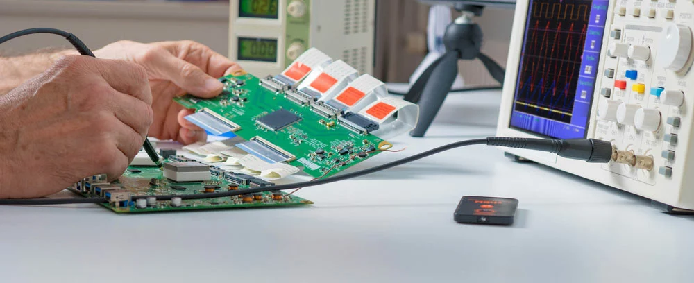
A man working on a PCB
A black pad occurs when a layer of dark nickel settles on the exposed areas of a PCB.
Unfortunately, this nickel layer forms during fabrication, especially when manufacturers overuse phosphorus in the gold deposition stage.
Also, black pads lead to oxidation and corrosion from the electroless nickel.
This situation becomes an issue during the assembly process.
As it worsens and corrosion spreads, it becomes harder to join various metal components.
As a result, manufacturers will experience low solderability and solder joints with weak integrity.
Sadly, those solder joints will break when strained and expose the rusted nickel underneath.
Why does Black Pad Happen?
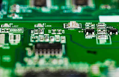
PCB
Several factors can cause black pads on PCBs.
Let’s explore some of them.
Gold Deposition Corrosion
The gold deposition is a crucial aspect of creating ENIG finishes in the PCB manufacturing process.
However, this process is one of the culprits for black pads.
Using aggressive gold baths on the PCB can kickstart speedy nickel corrosion, which causes the notorious black pad.
Also, a heavy gold thickness may cause this problem.
A PCB with excess gold on its surface finishes will lead to galvanic hyper-corrosion and the creation of black pads.
Excessive Phosphorus Content
High phosphorus content in the gold deposition, especially during reflows and soldering, can cause black pads.
In addition, excess phosphorus surface tends to permeate the nickel, causing oxidation.
Eventually, the process will activate delamination and crack solder joints, causing electrical shorts.
Brittle Fracture
A brittle fracture occurs when certain materials suffer from high stress, particularly when they can’t withstand pressure.
Stressed materials snap without warning and can cause several problems on a PCB.
Generally, a brittle fracture appears as a black pad.
Usually, brittle fracture occurs when tin transmutes into nickel.
This process creates a thin phosphorus layer that won’t dissolve, affecting the board’s metallurgical bonds.
In addition, vibrations, shocks, and thermal stress can also create brittle fractures.
Such situations will cause cracked structures inside the nickel, causing electrical shorts.
Black Pad Indications
Black Pad issues may be hard to pick out immediately. Usually, the immersion gold will hide the nickel under it. Also, you will likely miss the black pad signs until it’s time for quality assurance tests.
During the tests, you must pay attention to the following indications. They’ll indicate black pad PCB problems.
Erratic/Inconsistent BGA Test Results
BGA inspection comes during the Quality Assurance stage. The tester looks out for the connections between the chip and the PCB.
Normally, the tester doesn’t need to exert too much pressure on the chip to get accurate results. However, the surface finish won’t provide any readings unless you exert pressure if a black pad is present.
Discoloration
It would be best to have a keen eye to differentiate between discoloration caused by lead-free oxidation and oxidation from black pads.
The color similarity might present a challenge during inspection. However, a closer look will show a silver-grey color for lead-free oxidation.
On the other hand, the black pad presents a dull black or grey color. The texture is a bit grainy, too.
Think of something burned.
Also, the black pad has a hint of brown discoloration.
Non-Wetting
The black pad makes soldering difficult since the soldering joints become weak. Therefore, molten solder fails to bond to the material on the PCB board.
The net effect is no adhesion between the PCB and any components.
Cold Solder
Cold solder is a defect when solder doesn’t melt and form joints. Black pad makes cold solders more prevalent because there are no proper bonds on the PCB.
Inconsistent Reflow
Since the black pad affects bonding, reflow may fail to cover the PCB board. When you check the perimeter, you’ll know there’s a reflow problem during the BGA inspection.

Is Black Pad Still An Issue For ENIG?
Nickel and gold are crucial elements in ENIG finishing.
The black pad will always be a looming concern for ENIG.
Also, there’s the issue of phosphorus. The ENIG process has heavy phosphorus demands.
To that end, ENIG repairs that need high phosphorus usage increase the likelihood of a black pad.
How To Fix Black Pad
Unfortunately, the black pad is a damaging outcome that requires you to redo the PCB manufacturing process.
The best way to fix a black pad in PCB is to take a preventative approach. Manufacturers must closely monitor the finishing process to ensure the nickel bath is regulated to the right quantities. The gold immersion stage should maintain a balanced nickel-to-gold ratio.
Additionally, manufacturers can manage phosphorus to prevent it from accumulating and weakening the board as it leaves behind remains.
IPC-4552 ENIG specifications have gold thickness guidelines that limit the amount of gold you can use. The specifications allow a 2-4 thickness range for the gold bath. Keeping a low gold thickness prevents instances of black pads.
Fixing the black pad requires you to engage your ENIG providers. Since every ENIG provider has a different set of quality assurance processes, ensure you know their processes before manufacturing.
Request a small initial batch to verify their standards before going full-scale.
How to Prevent Black Pads
Sadly, it’s almost impossible to detect black pads during manufacturing–and that’s where the problem starts.
It becomes noticeable during assembly or when stressed joints and open circuits create a catastrophic issue.
But that’s not all.
You may not notice black pads until you attach components to the PCB unless you perform non-destructive tests on the board.
Therefore, preventing black pads is a critical responsibility of suppliers and manufacturers.
However, knowing that high phosphorus causes black pads is not the same as controlling these levels during manufacturing.
Here are some solutions manufacturers can use to prevent black pads:
- Verification of potential ENIG providers.
- Using chelating agents.
- Careful inspection of pH levels to ensure plating the adequate amount of phosphorous.
- The removal of oil and residues before the PCB etching process.
- Applying a well-controlled immersion gold process with a proper nickel-to-gold ratio.
- Avoid nickel plating out into tanks.
- Cleaning the suspicious black pad areas regularly.
Final Words
A black pad on a PCB can spell doom for the board.
Unfortunately, it’s almost impossible to detect during manufacturing and may become evident after mounting components.
However, partnering with a good manufacturer will help prevent black pads from plaguing your PCB.
Quality manufacturing services know how to avoid nickel corrosion during immersion gold plating.
Also, you can follow the solutions above to get specific instructions–for your designs.
Do you have any questions?
Feel free to contact us, and we’ll be happy to help.


