Contents
- 1 What Is a Low Loss PCB?
- 2 What are the Properties of Low Loss PCBs?
- 3 Low Loss PCB Materials
- 4 Where are Low Loss PCBs Used?
- 5 Standard vs Low Loss PCBs
- 6 What is a Low Loss PCB FAQs
- 6.1 What’s the difference between low loss and ultra low loss PCBs?
- 6.2 What industry standards should low loss PCBs meet?
- 6.3 How do low loss PCBs improve 5G performance?
- 6.4 Can low loss PCBs handle frequencies above 40 GHz?
- 6.5 How do you test low loss PCB reliability?
- 6.6 Are low loss PCBs more expensive to manufacture?
What Is a Low Loss PCB?
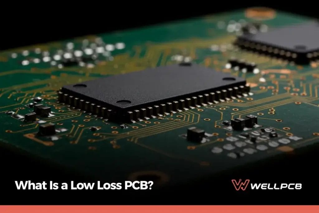
A low loss PCB is a printed circuit board specifically engineered to minimize loss of signal in high frequency signal transmission. Standard boards experience dielectric loss, copper loss and radiation that cause distortion and energy loss.
In contrast, a low loss PCB material like PTFE or ceramic-filled epoxy provides a low dielectric constant and low dissipation factor (Df), both of which improve impedance control and reduce insertion loss.
The result is a board that delivers low signal loss, stable transmission and improved thermal reliability compared to a standard PCB. Various industries use low loss PCBs to achieve cleaner signals and lower power consumption, keeping their customers happier and saving them money in the long run.
What are the Properties of Low Loss PCBs?
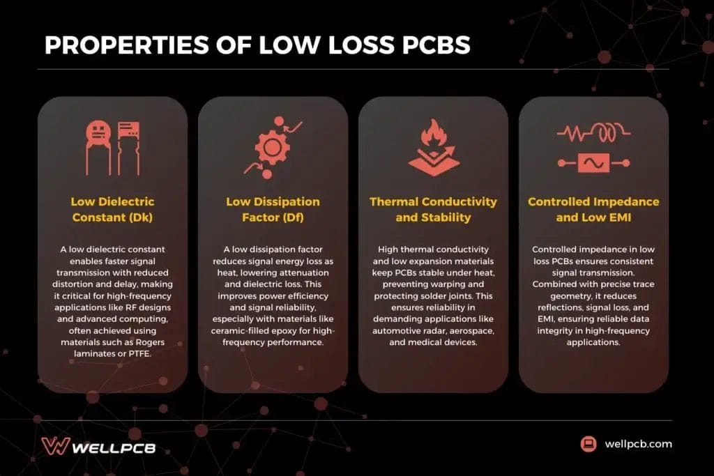
The performance of a low loss PCB depends on its material selection and how well it controls electrical and thermal behavior at high frequencies. Properties such as dielectric constant, dissipation factor, thermal stability, and impedance control directly influence how effectively the board can minimize signal loss and maintain reliability in demanding environments.
Low Dielectric Constant (Dk)
The dielectric constant (Dk) defines how a dielectric material stores and transmits electrical energy. In a low loss PCB, a low dielectric constant allows signals to travel faster and with less delay.
This property reduces distortion and loss, especially important for high-frequency applications such as RF PCB designs and advanced computing systems. Engineers often choose materials like Rogers laminates or PTFE, because they deliver low Dk values while maintaining stable electrical properties across high frequencies.
Low Dissipation Factor (Df)
The dissipation factor (Df, sometimes called the loss tangent) indicates the portion of signal energy that’s converted into heat as it travels through the PCB material. A low Df minimizes energy loss, which directly lowers attenuation and dielectric loss.
In practical terms, this means less wasted power and more reliable signal quality. The use of low loss PCB material like ceramic-filled epoxy improves performance by keeping the loss factor extremely low, even at high frequency signal ranges.
Thermal Conductivity and Stability
Low loss PCBs often incorporate materials with good thermal conductivity and a low coefficient of thermal expansion. This keeps their performance stable even at high temperatures.
This prevents warping, protects solder joints and maintains consistent dielectric properties during thermal cycling. Such stability is essential for automotive radar, aerospace systems and medical devices that operate under continuous load.
Controlled Impedance and Low EMI
In PCB design, controlled impedance ensures that signal lines maintain a consistent transmission profile. Low loss PCBs achieve this by combining carefully tuned board material properties with precise copper trace geometry.
Proper impedance control reduces reflections, minimizes signal loss and lowers electromagnetic interference (EMI). This makes low loss PCBs indispensable in high frequency applications where reliable data integrity is non-negotiable.
Low Loss PCB Materials
The choice of low loss PCB material determines how well a board performs at high frequencies. Different materials work best for different applications.
| Material | Typical Dk | Typical Df | Description |
|---|---|---|---|
| PTFE (Teflon) Substrates | 2.1 to 2.6 | ~0.0009 to 0.004 | Widely used for RF PCBs and ultra low loss PCBs. Offers excellent electrical stability but is more expensive and requires specialized processing. |
| Ceramic-Filled Epoxies | 3.2 to 3.8 | ~0.003 to 0.008 | Combine good mechanical strength with low dielectric loss and improved thermal stability. Common in automotive radar and aerospace systems. |
| Rogers Laminates (RO4000, RO3000 Series) | 2.9 to 3.5 | ~0.001 to 0.003 | Industry-standard low-loss PCB materials. Deliver low signal loss, consistent dielectric properties, and high reliability for high frequency signal transmission. |
| Liquid Crystal Polymer (LCP) | ~3.0 to 3.2 | ~0.002 | Flexible, stable at high temperatures, and used in advanced flex circuits. Excellent for miniaturized, high-frequency applications like smartphones and aerospace. |
Where are Low Loss PCBs Used?
The demand for low loss PCBs is high in industries where even minor signal loss or instability can compromise performance. From high speed communication networks to aerospace systems, these boards are chosen for their ability to maintain reliable transmission in harsh environments and deliver consistent results.
5G Networks and RF Systems
Low loss PCBs are foundational to 5G antennas and RF transmission lines, which often operate above 24 GHz. At these high frequencies, dielectric loss in standard FR-4 boards (~Df 0.020) causes severe signal attenuation.
In contrast, Rogers RO4350B (Dk ≈ 3.5, Df ≈ 0.0037) or PTFE substrates (Dk ≈ 2.2, Df < 0.001) maintain consistent impedance and reduce insertion loss by more than 50%. These materials also limit copper loss through smoother conductor surfaces, which is a necessity for RF PCBs in base stations and mmWave modules.
Aerospace Electronics
Radar arrays, avionics, and satellite payloads require low-loss PCBs that can operate under extreme thermal and mechanical loads. Materials with a low coefficient of thermal expansion (less than 20 ppm/°C) prevent warping and misalignment during rapid altitude and temperature shifts.
Ceramic-filled PTFE laminates are favored for high-frequency radar systems because they maintain stable dielectric properties up to 40 GHz and exhibit low dissipation even in radiation-heavy environments. Ultra low loss PCBs ensure that sensitive guidance and communication systems transmit without distortion.
Automotive Radar and ADAS
Automotive radar systems operate in the 77 to 79 GHz band, where even minor loss tangent increases can degrade range detection accuracy. Low loss PCB material like hydrocarbon ceramic laminates (Df < 0.004) provide low signal loss and controlled impedance routing for compact radar modules.
The advantages of low loss include faster response times for collision avoidance, stable PCB boards under wide ambient temperatures (-40°C to +150°C) and reduced energy loss in electric vehicle ADAS architectures.
Medical Imaging and Monitoring
MRI, and ultrasound systems demand low-loss PCBs that deliver precise analog signals with minimal distortion and loss. Materials like PTFE composites (Dk ~2.2, Df ~0.0009) enable higher resolution imaging by suppressing attenuation and dielectric loss during data transfer.
High thermal conductivity board materials prevent localized heating, ensuring continuous operation in equipment that runs for extended diagnostic sessions. The choice of material is especially important here, since any fluctuation in dielectric properties can compromise imaging accuracy and put lives at risk.
Data Centers and High-Speed Computing
In routers, switches, and server backplanes, low loss PCBs must handle data rates above 56 to 112 Gbps. Traditional standard PCBs introduce loss of signals at these speeds due to high loss factors. Low Dk laminates (Dk ≈ 3.0–3.5, Df < 0.003) support long trace lengths while keeping insertion loss within design margins.
These materials also reduce copper loss by allowing the use of smoother copper foils (eg. rolled annealed copper). By lowering energy loss, data centers achieve reduced cooling loads and more efficient PCB production for large-scale computing.
Consumer Electronics and IoT Devices
Miniaturized consumer devices rely on low loss PCBs for wireless connectivity and high speed interfaces. Liquid Crystal Polymer (LCP) substrates (Dk ≈ 3.0, Df ~0.002) are commonly used in smartphone antennas and wearables, offering stable dielectric constant and dissipation factor values even at GHz bands.
Their low moisture absorption (<0.04%) ensures low dielectric loss in humid environments. In IoT devices, this translates to low signal loss, reduced power consumption, and extended battery life.
Satellite and Space Systems
Ultra low loss PCBs are common in satellites and space probes, where transmissions span thousands of miles. Rogers RT/duroid 5880LZ (Dk = 1.96, Df = 0.0019) and other ultra low loss materials are commonly selected for payload communication systems.
Their combination of low dielectric constant and dissipation factor reduces attenuation and dielectric loss, ensuring maximum range with minimal distortion. Their low coefficient of thermal expansion and high thermal conductivity prevent material fatigue under space’s vacuum, radiation and extreme temperature cycling.
Standard vs Low Loss PCBs
The choice between a standard PCB and a low loss PCB depends on the operating frequency, performance requirements and application environment.
| Property | Standard PCB (FR-4) | Low Loss PCB |
|---|---|---|
| Dielectric Constant (Dk) | ~4.2 to 4.8 | 2.0 to 3.5 (varies by material) |
| Dissipation Factor (Df) | ~0.015 to 0.020 | 0.0009 to 0.004 |
| Signal Loss | Noticeable at >1 GHz; severe above 5 GHz | Minimal up to 40+ GHz |
| Copper Loss | Higher due to rough conductor surfaces | Reduced with smooth copper foils (eg. RA copper) |
| Thermal Stability | Moderate, prone to expansion and warpage | High, often uses materials with low CTE and high thermal conductivity |
| Impedance Control | Less precise, reflections increase at high speed | Tight control, stable impedance in high frequency signal routing |
| Applications | Consumer devices, general electronics | 5G networks, RF systems, aerospace, medical, data centers, automotive radar |
| Cost | Lower, widely available | Higher due to specialized materials and advanced PCB fabrication |
What is a Low Loss PCB FAQs
What’s the difference between low loss and ultra low loss PCBs?
Low loss PCBs have a dissipation factor (Df) in the range of 0.002 to 0.004, while ultra low loss PCBs use materials with Df below 0.001. Ultra low loss boards provide even lower insertion loss and are used in extreme high-frequency applications like satellite and deep space communication.
What industry standards should low loss PCBs meet?
They should comply with IPC-4101 for base materials, IPC-TM-650 for dielectric testing and IPC-A-600/610 Class 2 or 3 for fabrication quality. In regulated sectors, additional compliance may include UL certification, RoHS, REACH, and aerospace or telecom-specific standards.
How do low loss PCBs improve 5G performance?
By using low Dk and low Df materials, low loss PCBs minimize signal loss and distortion at high frequencies above 24 GHz. This improves antenna efficiency, extends range, and supports higher data throughput, making them vital for 5G base stations and mmWave modules.
Can low loss PCBs handle frequencies above 40 GHz?
Yes, with specialized materials such as PTFE and Rogers laminates, low loss PCBs can operate reliably above 40 GHz, provided the PCB design incorporates tight impedance control and smooth copper surfaces to minimize copper loss.
How do you test low loss PCB reliability?
Reliability is verified through insertion loss testing, impedance measurements and thermal cycling. Additional methods include environmental stress testing, X-ray inspection and microsection analysis to check structural integrity.
Are low loss PCBs more expensive to manufacture?
Yes, low-loss PCB material such as PTFE and LCP costs more than FR-4, and PCB fabrication requires tighter tolerances. While this raises production costs, the performance benefits often outweigh the expense.
Back to Top: What is a Low Loss PCB? Low Loss PCB Material & Features