Modern printed circuit boards (PCBs) are the lifeblood of technology today. It is nearly impossible to find electronics that do not have a PCB in some form. While it takes a professional PCB manufacturer to produce quality printed circuit boards, you can create your very own Homemade PCB. In the following guide, we will show you how.
Contents
Homemade PCB–What is a Printed Circuit Board?

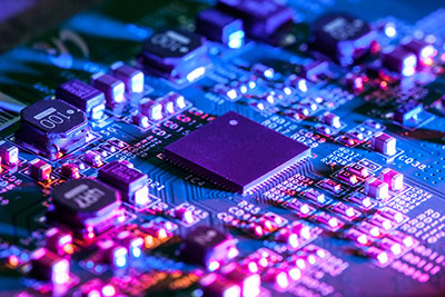
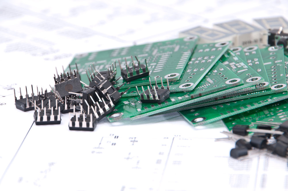
Image of printed circuit board with components
Printed circuit boards became widespread in the latter half of the 20th century. Before then, manufacturers connected the components of an appliance directly through wires. As such, it was disorganized and messy. The creation of PCBs sought to solve this issue.
In essence, a PCB is a collection of embedded wires running through a flat fragment of fiberglass. To understand how they work, you need to know how fabricators create them.
During the fabrication process, the manufacturer stacks slices of fiberglass together and treats them with a chemical resin, which bonds them together.
Next, the manufacturer will apply a copper layer to both sides of the fiberglass slab. Then, they will apply photoresist. The manufacturer will then etch a PCB layout pattern that matches the traces on the board. After that, they will harden and dry the board with UV light.
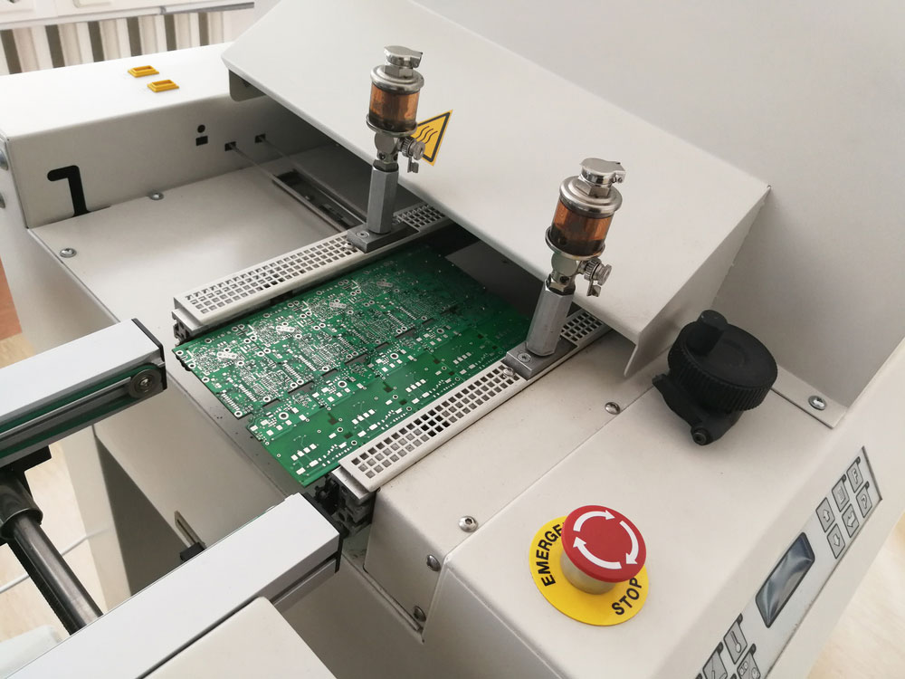
Printed circuit board after complete assembly moves to reflow oven machine
Next, the manufacturer will wash the board with warm which will wash away the uncovered areas, leaving the tracks of copper. These tracks will serve as a base for how the PCB will look after the copper etching process.
Depending on the board’s specifications and design, the manufacturer will drill mounting holes, through holes, and via holes for connections and components.
Nevertheless, because the PCB is just a collection of electrical connections on a substrate, you do not need any fancy manufacturing process to make a simple one. We will show you how in the rest of this guide.
Easy Ways To Fabricate A Circuit Board Yourself
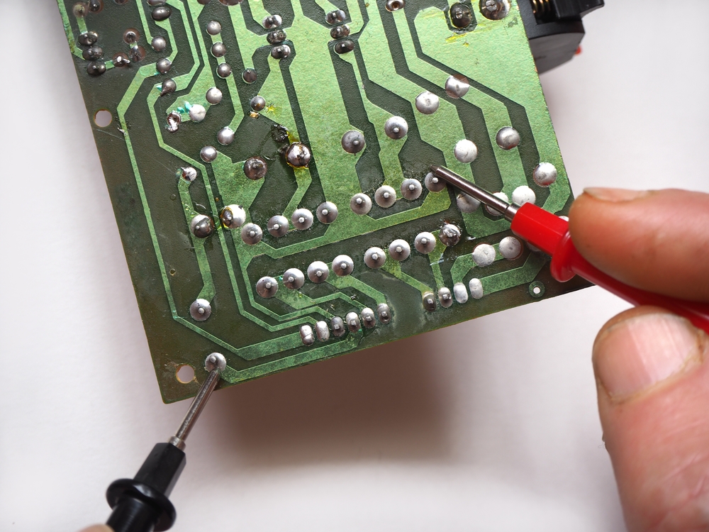
Printed circuit board.
It’s easier than it sounds to make your own circuit board at home. Try out some or all of these techniques to get started:
- Laser etching
- Drawing the circuit design on the board
- Use an iron and gloss paper
Homemade PCB– How To Make a PCB at Home?
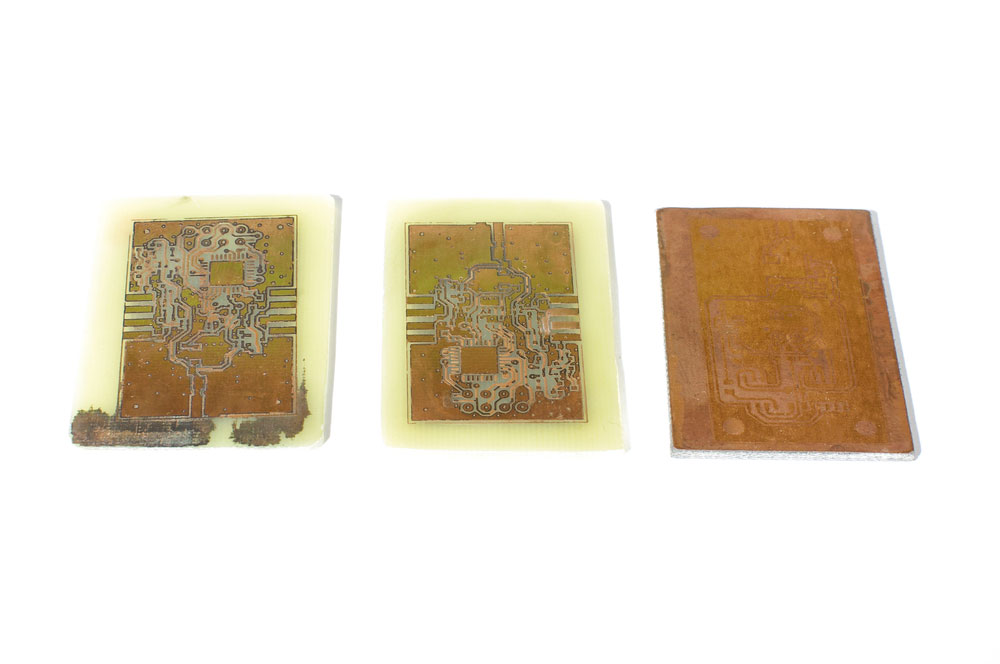
A collection of three copper-printed circuit boards.
This section of the guide will cover how to make your very own DIY PCB at home. We have included a list of all the materials you will need. However, in our estimation, the essential component you will need is PCB design software. Luckily, there is a host of great open-source design software to help you create your circuit designs. They include:
Each of these tools has tutorials and documentation to help you learn how to design PCB layouts. Once you have created and printed out your desired PCB design, you can proceed with the rest of this guide.

Sketching out a printed circuit board
Homemade PCB– Required Tools and Materials
- Old magazine paper or advertising brochures with glossy print
- Old newspaper
- Laser or inkjet printer
- Clothes steam iron
- Copper clad laminate sheet
- Ferric chloride powder solution (FeCl3 etching solution)
- Dish wash scrubs/steel wool
- Acetone (nail polish remover/ thinners)
- Rubber gloves
- Plastic box/ plastic container
- Teaspoon
- PVC wire
- A4 photo/glossy paper
- Sandpaper
- Black permanent marker
- Blade cutter
- Sandpaper
- A roll of paper towels
- Cotton wool
- Clear tape
- Brown Paper
- Oven Mitts
Instructions
For this tutorial, we have decided to keep things simple. We will be creating a PCB that connects to a 555 timer chip. Thus, you will be able to develop or integrate into your very own touch switch. Before proceeding with the instructions in this section, please ensure you have all the materials and tools.
A collection of chips, along with a set of circuit boards
Homemade PCB– Step 1
Use your inkjet or laser printer to print out the PCB layout you created using one of our recommended PCB design software tools. Make sure that it prints out in Black/Grayscale. You can configure the settings on the PCB design software and the printer driver settings.
Additionally, you must ensure that it’s a mirror printout. Furthermore, it must print out on the glossy side of the photo paper. Once it is printed, cut the design out from the article.
Printing PCB layout
Homemade PCB– Step 2
Cut a square piece from the copper-clad laminate using a cutter. When cutting, use the printed PCB layout as a size reference.
Homemade PCB– Step 3
Use steel wool or a kitchen scrub to rub the copper side of the cut-out laminate, removing the top oxide and photoresist layer. It will make it easier for you to stick the PCB layout design on the copper.
Homemade PCB– Step 4
Transfer the printed PCB layout onto the top of the treated copper laminate layer (which will serve as the final PCB). Ensure the glossy portion of the paper is facing down and aligned with the piece of copper laminate’s sides.
Homemade PCB– Step 5
Next, place the brown paper on top of the copper piece and printed design paper. Press and iron the design onto the copper piece, with the brown paper serving as protection. While doing this, you need to ensure:
- You are using a flat wooden or granite surface
- The iron is not set to steam
- Iron slowly while applying steady pressure
- The copper board is secure – you can use a pair of pliers

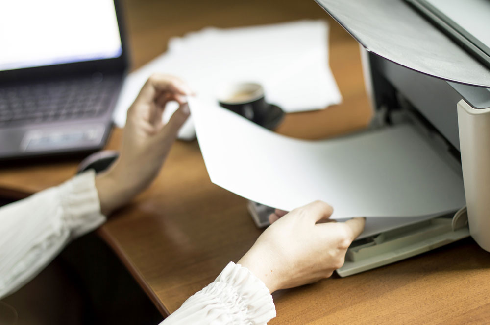
Image of clothes steams iron. Warm the clothes and iron them until they reach their maximum temperature.
If you do it properly, the entire transfer process will take an hour. However, if you are not comfortable using an iron, you can transfer the design onto the copper face using a pencil and a permanent black marker.
Step 6
Use oven mitts to transfer the copper piece into a bowl, sink, or container of lukewarm water. Next, leave it in the water for 10 minutes. Finally, gently separate the paper from the copper. The most effective way to do this is by peeling the report from the copper at a low angle.
Sometimes, the design may not wholly show up on the copper face. In that case, you will need to use your permanent black marker to fill out any missing lines.
Step 7
Next, we need to etch the plate. Put on a pair of rubber gloves and cover your floor, desk, and counter with brown paper or newspaper. Accordingly, this will prevent the etching solution from spoiling them.
Fill up a plastic container or box with water and place three teaspoons of ferric chloride powder into it. Carefully stir until you dissolve the solution. Next, dip the PCB (a copper piece) into the solution for thirty minutes or until the process unmasks the copper.
Use pliers to check if the etching process is complete. It should remove any unwanted copper from the final product.
Step 8
Once you have etched the PCB, dilute the rest of the ferric chloride solution and dispose of it carefully. Do not pour it down your drain or flush it down your toilet. It could damage your plumbing and pipes. If possible, contact a hazardous chemical collection service in your town.
Use a few drops of acetone (nail polish remover) on a piece of cotton wool to wipe away the ink/toner on the PCB to reveal the copper layout. Next, clean and rinse the PCB with warm water and dry it with a paper towel.
Finally, you can use sandpaper to trim and smooth the edges of the PCB. You can use a micro-electric drill to create through holes.
Alternatively, you can solder your electronic components directly on the PCB. If you want the PCB to have a more traditional look, you can purchase green or red UV-curable solder paint.
Once you have done that, all you must do is clean up your work area, and you have yourself a solid homemade PCB.
Printed circuit board without the components

4 DIY PCB Projects
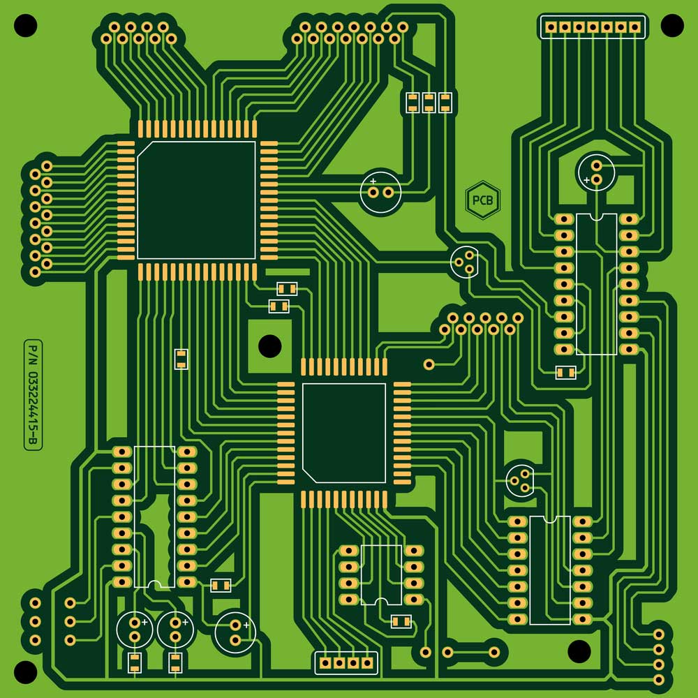
A circuit board on top of a diagram.
There are so many fun and creative cheap projects you can create. And they just require basic know-how to get everything going. Here are a few that may find their way into your everyday life!
Clap switch:
Everyone could use a handy clapping switch for their lights and other gadgets at home. When you clap, the circuit picks up that sound and turns your connected electronics on or off.
Fridge alarm:
This one is perfect if you or anyone else leaves the fridge door open for a long time. It blares out a beeping alarm in that scenario, alerting someone to close it.
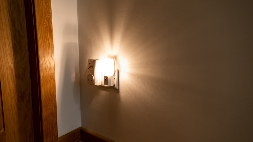
Nightlight:
Example of a nightlight.
You can create a nightlight PCB to help you see and move around at night. It uses common components, like an LDR and 555 IC, that will detect darkness and brighten up the room.
Rain detector:
These circuits are simple and meant to inform you when it starts raining. It uses an Attiny85 IC and rain sensor module to detect raindrops.
FAQs
Can anyone easily make a PCB?
It’s both hard and easy to make a PCB — depending on the project. But if you’re making something with a lot of components, then it gets harder to handle.
Is it possible to 3D print a printed circuit board?
A 3D printer can fabricate PCBs. For this to work, you may need to use aerosol jet printing to get the traces onto the board.
Are there ways to tell if your PCB goes bad?
Take a close look at your circuit board and components. A good sign of this is if you see any cracks, chips, corrosion, or burns.
Conclusion
Breadboards are great when you are still learning the ropes. However, you will find that actual solder-able PCBs are better for more complex projects.
Nevertheless, we hope that you have enjoyed reading this guide. If you want to learn more about the PCB manufacturing process, do not hesitate to visit the rest of our website. As always, thank you for reading.


