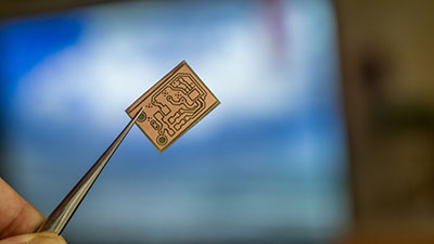
Printed circuit boards, also known as PCBs, in short, are what make all electronics to function as desired. Therefore, when something goes wrong on the printed circuit board. There are chances that the electronic device will not perform as intended. Printed circuit board problems are significant challenges for manufacturers since plenty of things can go wrong. Especially when it comes to the multilayer PCB fabrication process. Below is a list of 7 problems in the multilayer PCB fabrication process.
By knowing such issues, as a designer, you will put them in mind when building your printed circuit board, hoping to avoid them and subsequently bringing damage to your printed circuit board.
Contents
Design
When designing multilayer printed circuit boards, issues to do with bow and twist may come up. Bend and twist are some of the most common characteristics used in determining the flatness of PCBs. The bow aspect is a cylindrical or spherical curvature of the printed On the other hand, the twist is a condition that takes place when deformation lies somewhat parallel to the diagonal of your printed circuit board.
There are several steps that multilayer correct PCB service provider. Thankfully, there are various PCB manufacturing firms can take to avoid instances of bow and twist. First, multilayer PCB manufacturers need to use proper parameters when pressing multilayers PCBs to reduce the cases of stress on the printed circuit board. Secondly, they need to avoid mixing materials from several suppliers. Thirdly, the materials used should be those that meet RoHS guidelines. As a PCB producer, you’ll also need to use or employ horizontal ovens during the curing process to avoid issues to do with bow and twist on your PCB.
Pressing Multilayer PCBs
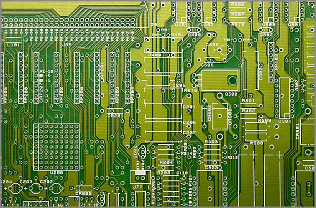
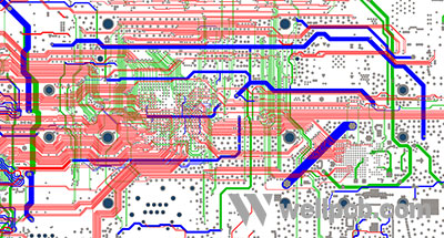
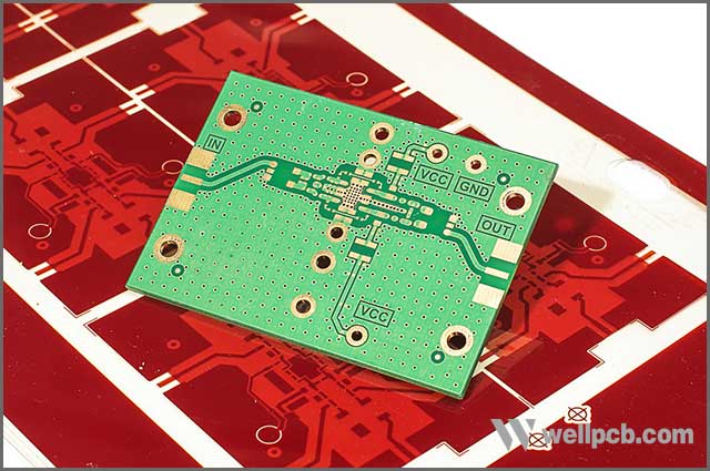
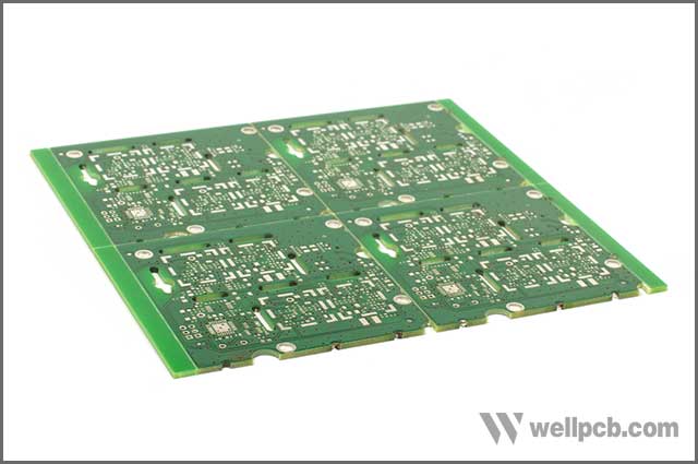
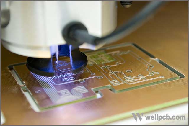
Multilayer printed circuit boards are those boards that contain more than a single layer counts, hence the need for stack-up. Stack-up is the arrangement of insulating and copper layers to make a printed circuit board before the PCB layout design.
When it comes to the manufacture of multilayer printed circuit boards, challenges come in when it comes to pressing the insulating and copper layers together. A majority of multilayer printed circuit board manufacturers tend to encounter difficulties when it comes to pressing multilayer printed circuit board components together.
To ensure that the stacking process of multilayer printed circuit boards goes well, manufacturers need to ensure that they use the best machines suitable for the job in addition to using the best laminate materials.
Selection of the Substrate Material
Printed circuit board materials play two essential purposes. First, they conduct electricity, and secondly, they offer insulation between the conducting copper layers. Therefore, it is easy to understand the reason why the selection of substrate materials is vital towards the failure or success of your printed circuit board. Apart from impacting the thermal behavior of your PCB. The documents that you use on your PCB will also affect the mechanical and electrical characteristics of your PCB.
1.Dielectric constant
Since a majority of printed circuit board functions gets determined by the substrate material. then it means that substrate materials that are featured by high frequency require their application in high-frequency and high-speed PCBs. However, high-frequency substrate materials have to meet small and stable dielectric constant.
2.Substrate properties
Additionally, the substrate material must also perform well when it comes to heat resistance. stability, impact strength, chemical resistance, and manufacturability. It is vital to ensure that the substrate material meant for high-speed and high-frequency printed circuit boards must feature or consist of low hygroscopicity. The copper foil also needs to conform to high peel strength.
3.Insulation
FR4, also known as FR-4, is one of the best versatile and low-cost multilayer substrate materials known for offering excellent performance. FR-4 materials provide some of the best electrical insulation that comes with high dielectric strength.
Multilayer PCB Fabrication– Resin-Plugged Via Manufacturing
The resin plugging process is a standard process across the printed circuit board industry, especially in high-frequency products that require large thickness and a high number of layers. Lately, the application of resin plugging process is becoming more extensive, to the extent of finding widespread use in HDI panels. It’s desirable to employ the use of resin plugging if the intention is to solve or do away with problems that cannot be solved by pressure-filling or green oil plugging resins.
When it comes to the manufacture of multilayer printed circuit boards, the resin plug hole is a problem that a majority of manufacturers face. However, the best way to solve such a problem is to use a vacuum plug machine.
Resin plugging is a preventive measure aimed at securing the vias from the unwanted flow of the solder material, especially during the soldering and assembly process. The primary use of resin, especially when it comes to the manufacture of printed circuit boards, is to clasp fibers together and protect them from outside factors.

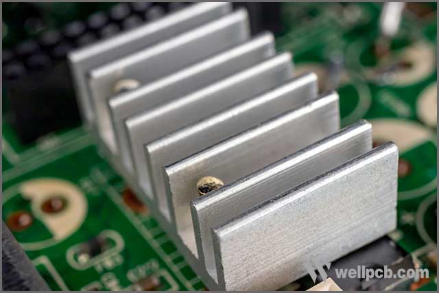
Dense Heat Dissipation Hole Manufacturing
When it comes to the manufacture of printed circuit boards, you may come across matters to do with heat dissipation. The Heat dissipation is a method of heat transfer. Heat dissipation happens when an object hotter than other purposes are placed or put in an environment where the heat of the more heated components transfers to the cooler objects. Heat dissipation occurs through several methods, chief among them being through convection, conduction, and radiation.
Issues to do with heat dissipation are problems that plenty of printed circuit board manufacturers face. However, to do away with dense heat dissipation, it is better to use the best or recommended heat dissipation materials such as aluminum.
Multilayer PCB Fabrication– Back Drilling Production
A Back drilling is one of the best manufacturing techniques commonly used on plenty of high-speed multilayers printed circuit boards to reduce or minimize the number of parasitics that are generated by plated through holes. Back drilling, also known as controlled depth drilling is a technique that enables you to eliminate some of the unused portions, stub, and copper barrel from a printed circuit board’s through- hole on the board.
The Back drilling reduces noise interference on the printed circuit board in addition to improving signal integrity and reducing the difficulty of manufacturing printed circuit boards. When it comes to the manufacture of multilayer printed circuit boards. back drilling is a big challenge that plenty of manufacturers face. Some of the most likely back drilling challenges to encounter include hole cleaning. barite sag, stuck pipe, loss of circulation, and shale instability.
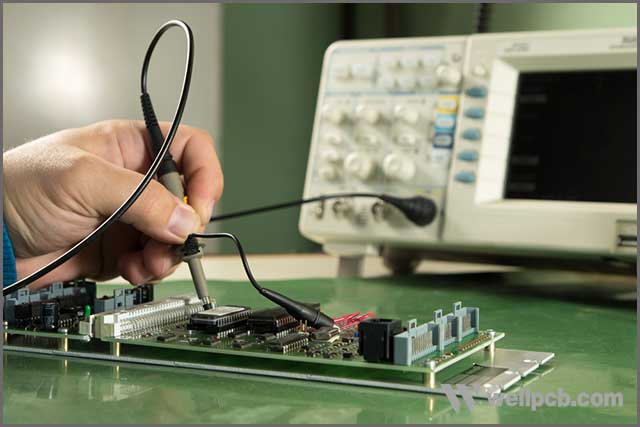
Multilayer PCB Fabrication– Testing
The testing phase of a printed circuit board is an essential part when it comes to the development cycle of PCBs. Conducted throughout the manufacture of printed circuit boards. testing printed circuit boards helps in saving money and preventing issues or difficulties when it comes to the final production run.
Unfortunately, when it comes to multilayer fabrication。 majority of PCB manufacturing firms fail when it comes to employing the best PCB test methods. Some of the best and recommended printed circuit board tests are bare-board tests, in-circuit tests, functional tests, and assembly level tests. Testing, especially in multilayer printed circuit boards, identifies or any technical defects within a printed circuit board.
Summary
There you have it, seven problems in the multilayer printed circuit board fabrication process. The next time that you want your multilayer printed circuit board made, you can trust us at WellPCB.
At need to know about ordering custom PCB Circuit boards online. FOR the PCB board you need, you can contact us at WellPCB, rest assured of high-quality multilayer board manufacturing experience in addition to strict testing procedures aimed at ensuring that the avoidance of the problems mentioned above.
WellPCB is a transparent company that keeps customer satisfaction at the first position. In case you have urgent multilayer printed circuit board orders, look no further than WellPCB.