

Figure 1 shows a table that elaborates the different thicknesses of the PCB board used b the designers.
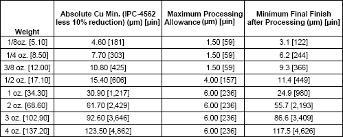
Figure 1
PCB Trace Thickness
The PCB trace thickness of any PCB board is chosen by the designer while designing the board. Commonly, the thicknesses chosen by the designer while designing four layers of PCB board are 0.020″, 0.031″,0.040″, 0.047″, 0.062″, 0.093″, and 0.125″ inches.
Users may select ½, 1, or 2-ounce inner layer of copper foil for their board. Figure 2 visually represents PCB’s trace thickness and how it varies before and after the components are etched into the board’s surface.
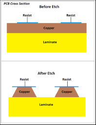
Figure 2
The thickness of the copper used plays a vital role in selecting PCB thickness, as they depend on each other. The unit of copper thickness used in the PCB board is ounce rolled on an area of 1 square foot.
Commonly, a PCB board that uses 1 oz copper has a thickness of 1.4 mils. Figure 3 shows the relationship between the width of copper used in PCB boards and the overall PCB trace thickness.
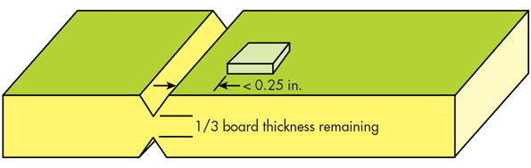
Figure 3

Conclusion
The significance of PCB thickness is equivalent, if not less, to that of a PCB board. The PCB thickness holds immense importance.
The designers perform many complex calculations to determine the depth of the PCB board that will deliver accurate results.
PCB trace thickness calculators are available to the designers to calculate the thickness of the PCB board immediately.
If the PCB trace thickness is wrongly calculated, the PCB may not achieve the accurate results it was designed for or damage the components attached to the surface of the PCB board.
The designer uses meticulous and precise techniques to ensure the accurate thickness of the PCB board.
Due to the accuracy of the PCB trace thickness, the material used during the design of PCBs is saved from being wasted or from over-use.


