
Contents
1. Etching(microfabrication)

In etching, a liquid (“wet”) or plasma (“dry”) chemical agent removes the uppermost layer of the substrate in the areas that are not protected by photoresist. In semiconductor fabrication, dry etching techniques are generally used, as they can be made anisotropic. To avoid significant undercutting of the photoresist pattern.
This is essential when the width of the features to be defined is similar. Or less than the thickness of the material being etched (i.e. when the aspect ratio approaches unity). Wet etch processes are generally isotropic, often indispensable for microelectromechanical systems, where suspended structures must be “released” from the underlying layer.
The development of the low-defectivity anisotropic dry-etch process has enabled the ever-smaller features defined photolithographically to be transferred to the substrate material.
2. Removal of photoresist

After etching or ion implantation, it is no longer necessary to use a photoresist as a protective layer, and it can be removed.
This usually requires a liquid “resist stripper,” which chemically alters the resist to no longer adhere to the substrate. Alternatively, the photoresist may be removed by a plasma containing oxygen, which oxidizes it.
This process is called ash and resembles dry etching. The use of 1-methyl-2-pyrrolidone (NMP) solvent for photoresist is another method used to remove an image. When the resist has been dissolved, the solvent can be removed by heating to 80 °C without leaving any residue.
The method of removing is classified as follows:
- Organic solvent removal: Removal of photoresist by organic solvent
2. Inorganic solvents: By the use of some inorganic solvents, the organic carbon in the organic matter of the photoresist is oxidized to carbon dioxide and then removed
3. Dry removal of photoresist: stripping photoresist by plasma
In addition to the main process, some auxiliary processes are often used, such as large-area uniform corrosion to reduce,e the thickness of the substrate, or remove the edge unevenly. Generally, in semiconductor chips or other elements, a substrate needs to be repeated many times.
3.Merits and demerits

The advantage of Photolithography Technology is that it can accurately control the formation of the shape, and size. Also, it can produce a profile on the whole wafer surface. However, the main demerit is that Photolithography Technology must be used on the plane. The rough surface of its effect will be worse. It also has a very high requirement of substrate cleaning conditions.
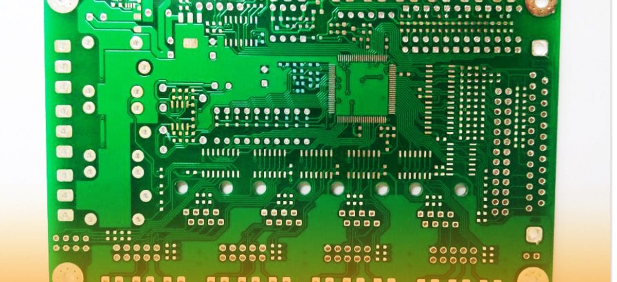
Figure – Photolithography for IC manufacturing