
Contents
Signal integrity for a good PCB design
From the signal analysis point of view on the PCB, one should note the maximum frequency. The corresponding rise and fall times of the signal. Inputs and outputs at the signals sourcing and sinking end, respectively. And single and differential-ended signals, analog and clock signals.
From a power supply point of view, the number of power supplies and their levels. And the required current, VCC sag, types of decoupling capacitors network, return or ground path and the ground bounce. Make thickness of power supply and ground tracks.

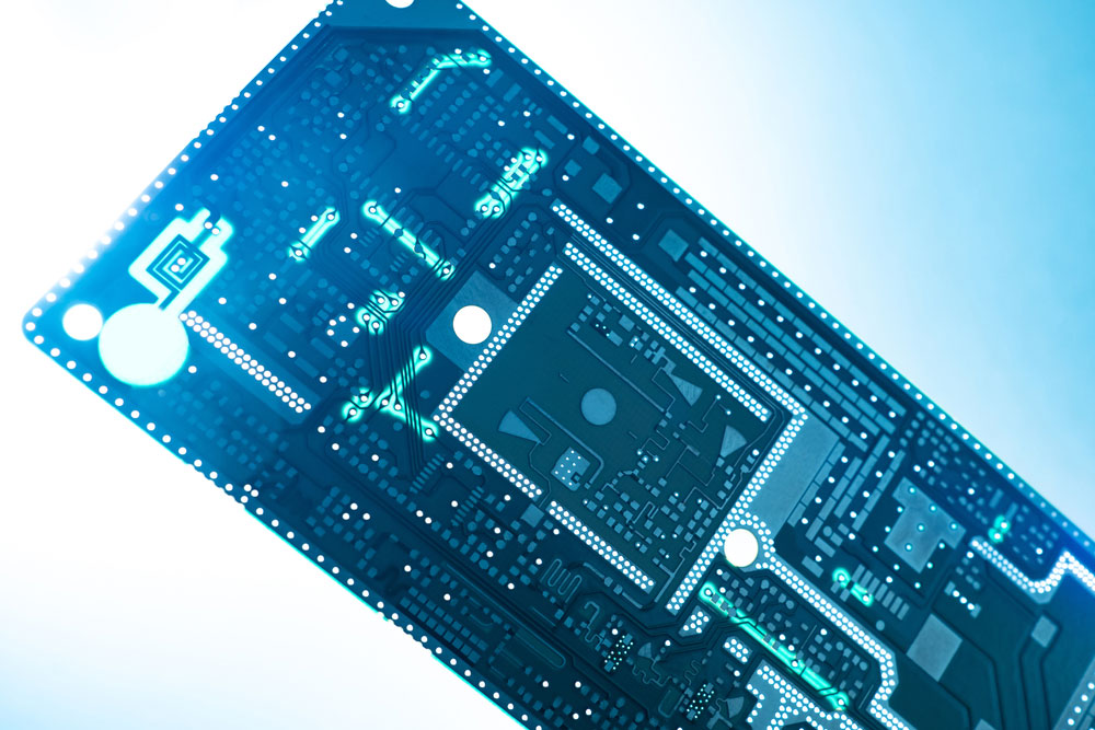
Signal integrity In PCB layout and design.
The digital, analog, and power supply components should be placed apart and appropriately. The analog and digital grounds should be separately managed and connected at a single thin point. The power supply plane should be split properly.
The signal layers should be routed at right angles to each other so that minimum crosstalk between signals would be minimized.
Avoid right angle traces to reduce the radiation, separate the analog, high-speed digital and clock signals, and provide sufficient clearance.
Between two tracks to reduce signal crosstalk and interference. Avoid vias whenever possible in the single-ended tracks; avoid vias in differential signals.
If necessary, add the same number of vias in both signals of the differential ended signals, route differential ended signals side by side.
Signal integrity issues are resolved at the very first level of circuit design and PCB layout.
Once the PCB is manufactured, the signal integrity issues are tough to resolve and require the next design review and manufacturing.
An IC package or PCB designer removes signal integrity problems through these techniques:
- Placing a solid reference plane adjacent to the signal traces to control crosstalk
- Controlling the trace width spacing to the reference plane to create consistent trace impedance
- The route traces perpendicular on adjacent layers to reduce crosstalk
- Providing sufficient ground (and power) connections to limit ground bounce (this subdiscipline of signal integrity is sometimes called out separately as power integrity)
- Adding a preemphasis filter to the transmitter-driving cell
- Improved clock and data recovery (CDR) circuitry with low jitter/phase noise
Each of these fixes may cause other problems.
This type of issue must be addressed as part of design flows and design closure.


