Aerospace PCB Assembly for Extreme
Reliability and Harsh Environments
Aerospace PCB assembly delivers ultra-reliable circuit performance for electronic systems in aerospace applications, where every solder joint and trace must perform under severe stress. With over 18 years in aerospace PCB fabrication, WellPCB manufactures certified assemblies that withstand the harshest conditions from flight systems to satellite operations.
- Aerospace PCB assembly with IPC-A-610H, AS9100, and ISO 9001 certification
- Advanced manufacturing for avionics, satellite navigation, and power converters
- Proven reliability for mission-critical aerospace electronic components

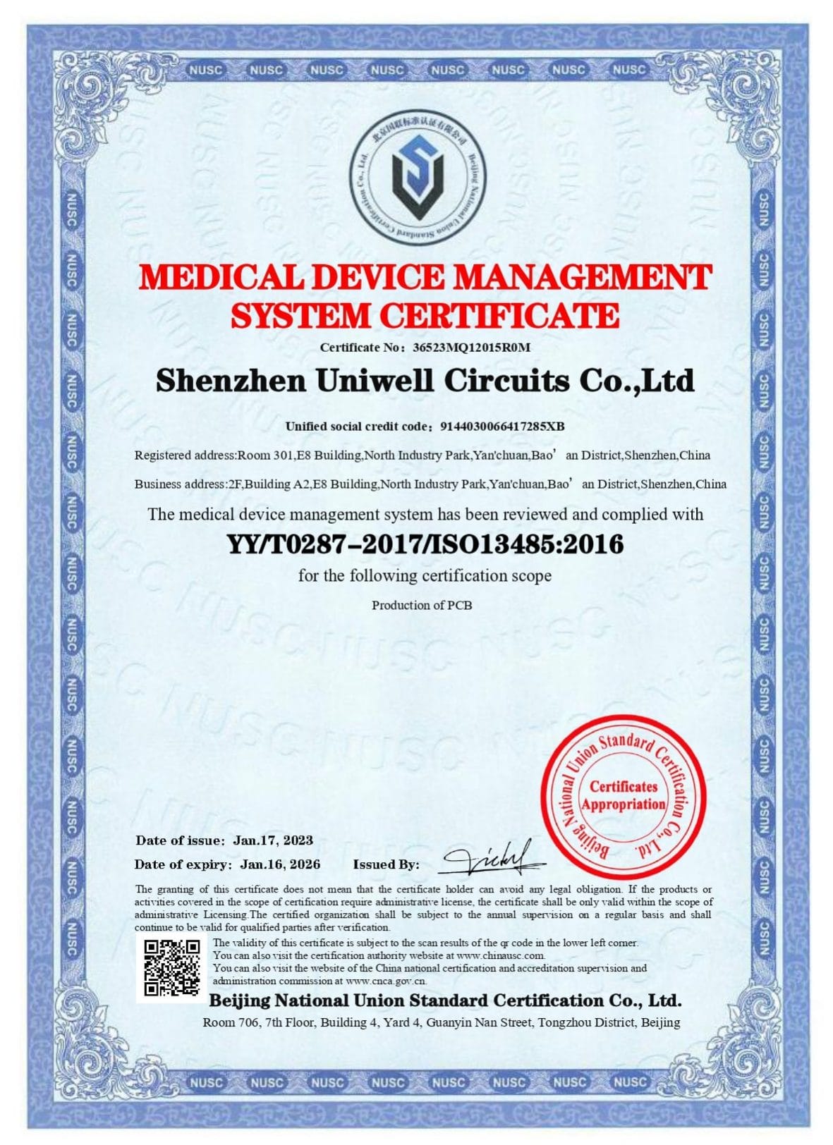
ISO9001 ISO13485
ISO14001

IATF
16949

IPC-A-610H International
Certification

Fully Automated
AOI Inspection
- PCB Manufacturer
- PCB Assembly Service
- Aerospace
Aerospace PCB Assembly
Services You Can Trust
Aerospace PCB assembly supports flight, satellite, and defense systems where mechanical and electrical reliability are non-negotiable. These PCB assemblies are designed to meet the stringent acceptance criteria of IPC-A-610 Class 3A and IPC-6012DS, providing consistent performance in mission-critical aerospace electronic components.
WellPCB specializes in PCB assemblies for aerospace systems, including flight control modules, satellite telemetry, RF navigation, and power converters. Our aerospace PCB assemblies utilize advanced substrates including polyimide, PTFE, and ceramic materials engineered for extreme temperature performance from -65°C to +125°C, with thermal shock testing capabilities up to 288°C.
Our manufacturing capabilities support complex PCB structures up to 64-layer rigid and 30-layer rigid-flex configurations using heavy copper (up to 1000 μm) for optimal thermal management and current load stability. We achieve precision SMT placement down to 0.2 mm pitch with ±30 µm accuracy and validate 2000+ thermal cycle tolerance for long-term reliability.
Our production flow includes nitrogen-assisted reflow soldering, comprehensive validation through 3D automated optical inspection, X-ray analysis, and in-circuit electrical testing. Each assembly receives conformal coating protection using acrylic or Parylene materials to harden against vibration, pressure changes, and extreme temperature cycles. We maintain full traceability down to each assembly component throughout the manufacturing process.
We support PCB fabrication and full assembly for aerospace PCBs using Rogers, Teflon, and FR408HR laminates to meet the diverse material requirements of aerospace applications.
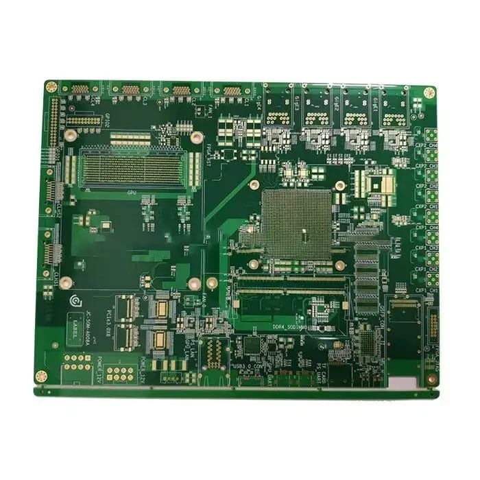
Our Aerospace PCB Assembly Capabilities
WellPCB provides aerospace PCB assembly services engineered for environmental endurance, signal integrity, and inspection traceability. Our process integrates strict IPC Class 3A workmanship criteria, certified materials, and design controls to support long-duration aerospace missions and defense-grade reliability.
Our aerospace PCB assemblies are rated to function across -65°C to +125°C ambient operating ranges, with thermal shock tests executed at 288°C for 10 seconds, repeated over three nonconsecutive cycles.
We use high-Tg laminate systems such as FR408HR (Tg 180°C), RO4003C (Tg 280°C), and RT/duroid 5880, validated for high-speed operation during rapid altitude transitions.
Vacuum-compatible solder alloys and heat cycle simulation chambers verify stability across 2000+ thermal cycles.
| Parameter | Specification |
|---|---|
| Operating Temperature Range | -65°C to +125°C |
| Thermal Shock Test | 288°C × 10 seconds × 3 cycles |
| Thermal Cycle Endurance | 2000+ cycles |
| High-Tg Material Examples | FR408HR (Tg 180°C), RO4003C (Tg 280°C), RT/duroid 5880 |
| Solder Alloy Compatibility | Vacuum-compatible, high-reliability lead-free alloys |
| Environmental Simulation Method | Chamber-based heat cycling and vacuum testing |
We achieve SMT pad densities supporting 0.2 mm BGA ball pitch, 0.15 mm QFP lead widths, and 0.35 mm fine-pitch spacing.
Our aerospace soldering platforms feature SPI solder paste volume control (±10%), 3D AOI coplanarity checks, and X-ray layer registration accuracy to 5 µm.
Surface tension integrity is validated using HIP defect reduction via nitrogen reflow at reflow setpoints of 245°C ±3°C with 60 ppm O₂ levels.
We fabricate up to 64-layer rigid PCBs with dielectric height control of ±10%, and up to 30-layer rigid-flex stackups using polyimide base films (eg. Shengyi SF305, 1 mil/0.5 oz).
Our flex PCBs are built with adhesive-less structures and coverlay precision to ±0.05 mm. We support dynamic bend radius ratios down to 10:1 and flex segment thicknesses as low as 0.08 mm, used in UAV avionics and curved spacecraft enclosures.
PCB aerospace builds requiring current handling above 10 A/inch trace width use copper thicknesses from 0.33 oz to 28 oz.
Copper layer uniformity is maintained at ±12% using electroplating profiles calibrated to 25 to 30 ASF.
We design power planes with thermal relief spokes, controlled via Polygon Pour configuration, and use thermal vias (0.3 mm drill, 1.0 mm pitch) with up to 16 via arrays per hotspot region.
Aerospace assemblies are finished with MIL-I-46058C-compliant coatings including acrylics (service -65°C to +125°C), silicones (up to +200°C), and Parylene-C (down to 1 µm uniform coverage with dielectric constant ~3.15).
Coating processes are applied under humidity-controlled laminar flow booths. We support masking for selective application and include UV-traceable inspection post-curing with ASTM D3363 hardness verification.
For satellite platforms, we integrate RO3003 or TMM10 substrates with double-sided copper shielding planes, maintaining EMI suppression under cosmic particle flux exposure.
Impedance-controlled traces are calculated using field solver tools (eg. Polar SI9000), with ±5% tolerance for 50 Ω single-ended or 100 Ω differential pairs.
Trace skew control is maintained under 25 ps with matched lengths and layer-symmetrical routing paths.
Each aerospace assembly undergoes 3D X-ray inspection (axial, planar, and BGA solder profile), ICT with bed-of-nails or flying probe up to 500 net points, and FCT simulating signal logic, load response, and input-output behavior.
Thermal aging simulates 1500 hours of continuous operation at 85°C. Additional tests include peel strength ≥1.4 N/mm, drop test to 1.2 m over 6 axes, and vibration testing up to 20 G at 100 Hz.
Connectors for aerospace PCB assemblies include MIL-DTL-38999, ARINC 600, and micro-D interconnects with gold-plated contacts (30 to 50 µin).
Stiffeners are bonded using thermally activated adhesive film with 1.5 mm ±0.2 mm thickness and edge clearance control to 0.5 mm.
Strain relief beading is applied for flexible tails used in avionics data buses and sensor packages in aircraft control systems. Automated silicone dispensing systems apply it with a bead diameter consistency of ±0.1 mm.
Why Choose WellPCB For Your Aerospace PCB Assembly?
WellPCB is an aerospace PCB manufacturer with proven experience in high-reliability PCB fabrication and assembly services for electronic systems in aerospace applications. Our facilities meet AS9100 (aerospace-specific quality management system), ISO 9001, and IPC-6012DS (performance and qualification spec for rigid aerospace PCBs) standards, with all aerospace assemblies built under full turnkey electronic production lines.

AS9100 and IPC-6012DS Certified Production

Multi-Stage Inspection and Test Coverage

High-Frequency and Hybrid Stackup Fabrication

Design for Manufacturability (DFM) Engineering Review

Traceability, Serialization, and Process Logging

Scalable Production with Component Sourcing
What Are Aerospace PCBs?
Aerospace PCBs are printed circuit boards built for high-reliability performance in aerospace environments where thermal shock, radiation, and vibration exceed commercial tolerances. These boards use high-Tg laminates like FR408HR, RO4003C, or RT/duroid 5880 to withstand -65°C to +125°C operating ranges and thermal shock up to 288°C.
Designed for avionics, satellite telemetry, RF systems, and power regulation, aerospace PCBs feature controlled impedance traces, redundant vias, thermal via fields, and MIL-spec components. Finishes such as ENIG or Parylene coating protect against oxidation, outgassing, and radiation effects in vacuum or high-altitude aerospace environments.
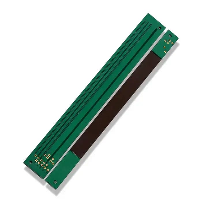
Features of Aerospace PCBs
Aerospace PCB assemblies are engineered to meet extreme reliability standards across high-altitude, orbital, and defense applications. Each feature supports long-term performance under vibration, radiation, thermal cycling, and limited-access maintenance conditions.

IPC Class 3A Solder Joint Integrity
All aerospace PCB assemblies meet IPC-A-610 Class 3A workmanship, requiring void-free solder joints with full barrel fill, coplanarity control under 50 µm, and minimum solder fillet height thresholds per component class.

High-Tg and Low-CTE Material Systems
Aerospace PCBs must withstand thermal gradients and mechanical strain. Laminates like FR408HR, RO3003, and TMM10 provide Tg values up to 280°C and low expansion coefficients for via reliability during thermal cycling in re-entry heat shields and orbital maneuvering avionics.

Heavy Copper and Thermal Via Integration
To handle power dissipation and transient current loads, aerospace PCBs use 2 to 4 oz copper planes with thermal via arrays (0.3 mm drill, 1.0 mm pitch) to distribute heat and stabilize circuit temperatures during mission peaks, such as in satellite payload converters.

Radiation-Resistant Substrates and Shielding
Boards used in space applications integrate RT/duroid or ceramic dielectrics with dual copper planes to reduce EMI and particle disruption in high-orbit satellite telemetry systems and RF communication modules.
Surface finishes are selected to minimize atomic oxygen and UV degradation.

Conformal Coating and Environmental Protection
Assemblies receive conformal coating in acrylic, silicone, or Parylene-C types depending on the aerospace application. Coatings are MIL-I-46058C compliant and applied under humidity control to ensure film uniformity and edge coverage.

Rigid, Flex, and Rigid-Flex Configurations
Rigid-flex PCBs reduce interconnect failure risk in compact enclosures. We support up to 30-layer rigid-flex stackups with laser-drilled microvias, polyimide flex cores, and resin-filled via-in-pad for BGA stability, used in modular satellite buses and curved fuselage-mounted control interfaces.

Vibration and Mechanical Stability Design
To resist vibration, aerospace PCB assemblies incorporate mechanical stiffeners, optimized mounting hole placement, and bonded connector zones. PCBs are tested under vibration loads up to 20 G at 100 Hz sinusoidal frequency.

Stringent Quality Standards and Traceability
Each build follows AS9100D and IPC-6012DS aerospace pcb design standards. Serial numbers, batch trace logs, and inspection results are retained for every aerospace PCBA, meeting full documentation and QA audit requirements.
Design Considerations for Aerospace PCB Assembly
Aerospace assemblies require strict adherence to electrical, thermal, and mechanical parameters to meet IPC Class 3A and AS9100 reliability standards.
| Design Parameter | Specification / Consideration |
|---|---|
| Signal Integrity | Controlled impedance to ±5%; matched trace lengths with skew under 25 ps for differential pairs. |
| EMC and EMI Management | Ground planes, shielding layers, and separation of analog/digital circuits according to EMI zones. |
| Thermal Management | Use of 2 to 4 oz copper, thermal vias, and high-Tg materials (≥180°C) to prevent overheating. |
| Vibration Resistance | Stiffener placement, resin-filled vias, and secure connector zones for mechanical reinforcement. |
| Component Selection | MIL-spec, high-temperature-rated components with shock and vibration tolerance qualifications. |
| Material Choice | Low-CTE laminates (eg. RO4003C, Teflon, FR408HR) for via and trace stability under cycling. |
| Via Structures | Laser-drilled microvias, via-in-pad, and stacked via combinations for interconnect density. |
| Coating and Protection | Selective conformal coating (Parylene, silicone) applied with film uniformity control < ±0.1 mm. |
Materials Used in Aerospace PCBs
Material selection is foundational to aerospace PCB reliability, with each substrate, coating, and finish chosen to withstand temperature gradients, radiation, and vibration across aerospace and defense environments.

Core Substrates
- Polyimide (PI): Used in rigid-flex builds for high durability and thermal endurance (Tg > 250°C).
- RT/duroid 5880: PTFE-based material with ultra-low dielectric loss, ideal for RF aerospace applications.
- RO4003C / RO4350B: Low-loss thermoset laminate for high-frequency circuits requiring impedance stability.
- FR408HR / Nelco N7000-2HT: High-Tg FR4 materials for mixed-signal aerospace PCBs up to 32 layers.

Dielectrics and Laminates
- Teflon/PTFE Composites: Provide stable Dk across -65°C to +125°C with minimal moisture absorption.
- Ceramic-Filled Epoxies: Used in aerospace and defense PCB builds needing dimensional stability under thermal shock.
- Hybrid Stackups: Combine ceramic, FR4, and copper to balance signal performance, rigidity, and cost.

Surface Finishes
- ENIG (Electroless Nickel Immersion Gold): ±5 µin thickness uniformity, ideal for BGA pads and fine-pitch assembly.
- ENIPIG: Combines wire bond compatibility with high corrosion resistance for aerospace electronic components.
- Immersion Silver: Used in low-EMI, high-signal integrity builds for space communication boards.

Conformal Coating Materials
- Acrylic: -65°C to +125°C operation, UV-traceable for inspection, fast curing, low-cost protection.
- Silicone: Supports up to +200°C continuous exposure with flexible adhesion under mechanical strain.
- Parylene C: Applied via vapor deposition for uniform barrier coverage in high-radiation aerospace assemblies.
Applications of High-Frequency PCBs
1. Solder Paste Printing
- Stencils: Nano-coated or step-up/down for critical pad volume control
- Paste: High-temperature, low-voiding alloys certified for aerospace-grade profiles
2. 3D Solder Paste Inspection (SPI)
- Inspection resolution: ±10% volume accuracy
- Detects insufficient paste, bridging, and pad misregistration
3. Component Placement
- Machines: ±30 µm placement accuracy at 3σ
- Supports BGA, QFN, CGA, PoP, and ultra-fine pitch components down to 0.2 mm
4. Nitrogen Reflow Soldering
- Profile: Peak temperature 245 to 255°C with O₂ concentration <60 ppm
- Reduces oxidation, flux residue, and HIP defects, improving long-term solder joint reliability in launch-vibration environments.
5. 3D X-Ray Inspection
- Verifies solder joint voids, hidden BGA defects, and component coplanarity
- Analysis resolution: <5 µm for multilayer PCB assemblies
6. 3D Automated Optical Inspection (AOI)
- Detects tombstoning, polarity errors, skew, insufficient solder, and lifted leads
- Coverage: 100% of visible solder joints
7. Conformal Coating Application
- Type: Acrylic, silicone, or Parylene, depending on mission exposure
- Applied under laminar flow with UV inspection and thickness tolerance <±0.1 mm, ensuring full coverage in high-altitude or vacuum conditions.
8. Final Functional and Environmental Testing
- Includes ICT, thermal shock, vibration (20 G, 100 Hz), and drop testing
- Validates full aerospace PCB assembly against customer-defined profiles
How to Order Your Aerospace PCB Assembly
in 5 Easy Steps

Submit Your PCB Design
Upload your Gerber files or use our easy online PCB design tool to create your board layout. Make sure your files are complete and correctly formatted to ensure smooth processing and production accuracy.

Select Your PCB Specifications
Customize your order by choosing the technical specifications—number of layers, board dimensions, thickness, copper weight, solder mask color, surface finish, and more. Our intuitive interface helps you configure everything based on your project’s needs.

Get an Instant Quote
Once your design and specs are in place, you'll receive a transparent, instant quote. Pricing updates in real time as you modify options, so you can adjust your selections to match your budget before placing the order.

Confirm Order & Make Payment
Review your entire order for accuracy, including file previews and selected specs. After confirmation, proceed to secure checkout and choose your preferred payment method. You’ll receive an email confirmation with order details.

Production & Delivery
Your PCB moves into production immediately. We’ll keep you updated throughout the manufacturing process. Once completed, your boards are carefully packed and shipped to your door, with tracking information provided for your convenience.
WellPCB is trusted by millions of
businesses and innovators.


Why Choose WellPCB?
WellPCB stands out among USA PCB manufacturers by delivering superior quality, advanced solutions, and unmatched reliability. With years of experience serving global markets, WellPCB has earned a reputation as one of the top PCB manufacturers in USA.
WellPCB specializes in multilayer PCBs for advanced electronic applications. You can order these boards with $100 off using our special offer, providing high complexity at competitive rates for demanding projects.




Hommer Zhao
Founder and Chief Editor – Hommer Zhao
Welcome! I’m Hommer Zhao, the founder and Chief Editor of WellPCB. With years of experience in the PCB industry, I’m committed to making sure our content is both accurate and helpful. We’re proud to serve a growing community of over 4,000 customers worldwide, and our goal is to provide you with the best resources and support. Your satisfaction is our top priority, and we’re here to help you every step of the way!

Jesse Holland
Technical Manager – Jesse Holland
Hi, I’m Jesse Holland, an Engineer and Technical Manager at WellPCB. With years of experience in PCB design and engineering, I’m here to ensure that every project we work on meets the highest technical standards. I lead our team, focusing on precision and innovation, collaborating closely with clients to provide tailored solutions and expert guidance. Whether you’re facing a complex design challenge or need advice on technical aspects, I’m here to ensure your project is a success from start to finish.

Nathan Jensen
Purchasing Manager – Nathan Jensen
Hi, I’m Nathan Jenson, the Purchasing Manager at WellPCB. I’m responsible for sourcing the best materials and components to ensure our products meet the highest quality standards. With my extensive experience in procurement, I work closely with suppliers to secure reliable and cost-effective solutions while maintaining strong relationships to support our operations. I aim to ensure every project runs smoothly by providing the resources needed to deliver on time and to your satisfaction.

Emma
Sales Manager – Emma
Hey, I am Emma, sales manager at WellPCB. I studied electronic science and technology at university and have served customers for PCB and PCB Assembly service for several years.
I enjoy communicating with customers and our technicians to solve problems, and customers always say, "It's great to have you onboard".
It is my pleasure and honour to be helpful. Contact me now, and you'll know.

Bella and Cassiel
Sales Representatives – Bella and Cassiel
We’re Bella and Cassiel, your dedicated sales representatives at WellPCB. With our extensive knowledge of the PCB industry, we’re here to provide exceptional service and support. We take the time to understand your unique needs and are always ready to offer tailored solutions and advice. Whether you need product recommendations, assistance with your orders, or simply have a question, we’re here to ensure your experience is smooth and seamless at every step.

Mandy and Wendy
Sales Representatives – Mandy and Wendy
We’re Mandy and Wendy, your friendly sales representatives at WellPCB. Passionate about helping our customers, we bring a wealth of experience in the PCB industry to provide you with the best solutions and service. We take pride in building strong relationships with our clients, understanding their specific needs, and offering personalised support to ensure their satisfaction. Whether you’re looking for advice, product information, or assistance with any part of your order, we’re here to make your experience as smooth and efficient as possible.
Our Team
Our skilled engineers and technicians bring expertise and precision to every PCB assembly project. Committed to quality, efficiency, and innovation, our team ensures every order meets the highest UL, IPC, ROHS & REACH standards, delivering reliable solutions tailored to your needs.
- Founder and Chief Editor – Hommer Zhao
- Technical Manager – Jesse Holland
- Purchasing Manager – Nathan Jensen
- Sales Manager – Emma
- Sales Representatives – Bella and Cassiel
- Sales Representatives – Mandy and Wendy
Aerospace PCB Assembly Case Studies

Case Study
This 10-layer rigid-flex PCB was custom-developed for a mission-critical aerospace system, requiring a combination of high signal integrity, lightweight construction, and mechanical resilience. With precise impedance control and a 4/6mil line width/space, the design supports high-speed signals and compact layout demands.
Product Specifications:
- Layer Count: 10 layers (Rigid-Flex)
- Structure: Multilayer rigid core with flexible interconnects
- Line Width / Spacing: 4 mil / 6 mil
- Impedance Control: Yes – Customized for differential/single-ended traces
- Application Industry: Aerospace – Flight control, navigation, and avionics systems

Case Study
This project features a 16-layer high-frequency PCB, specifically designed for aerospace applications requiring complex signal routing, low-loss materials, and advanced backdrill processing. Built with TU872SLK high-speed laminate, this board meets stringent requirements for signal integrity, thermal stability, and mechanical reliability in extreme aerospace environments.
Product Specifications:
- Layer Count: 16 layers
- Material: TU872SLK (low-loss, high-frequency)
- Inner Layer Spacing: 5 mil
- Backdrill Groups: 8 total: 1-2, 1-4, 1-6, 1-11, 16-4, 16-6, 16-8, 16-13
- Backdrill Isolation Layer: 4 mil
- Stab (Stub Length Control): 2 mil
- Application Industry: Aerospace – Radar, avionics, satellite systems
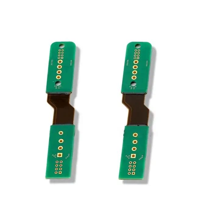
Case Study
This Flex-Rigid PCB solution was developed for aerospace applications, combining the mechanical strength of rigid boards with the adaptability of flexible circuits. With a large board size of 465 × 173 mm and a 3.0 mm thickness, it is designed to meet the needs of complex aerospace subsystems where compact integration and vibration resistance are crucial.
Product Specifications:
- Application: Aerospace Systems
- Board Structure: Combination of Rigid & Flex Layers
- Board Thickness: 3.0 mm
- Board Size: 465 mm × 173 mm
- Surface Treatment: HASL (Hot Air Solder Leveling)
Aerospace PCB Client Feedback
As an R&D manager, I have had an outstanding experience working with WELL-PCB. For many years, our company has entrusted them with the production, assembly, and programming of the boards developed in our R&D unit, and they have consistently exceeded our expectations.
Hamid Reza Moshayedi
R&D Manager
Their work is very impressively perfect. Today, when they check our company PCB board after assemble. They found a fake short point which many engineers has never found in the past years. But that is just designed so. The PCB board quality is excellent. Their service is also excellent.
MikeZ
My friend introduced WellPCB to me, the first try, a little look forward to. I ordered a 47*72 10ps PCB, and I can’t wait to receive my PCB. So I used expedited service and received my PCB in three days. I tested and soldered the PCB, Quality is really good, silkscreen, plating also great.
Warren Cliton
Aerospace PCB Assembly FAQs
What makes aerospace PCB assembly different from standard PCB manufacturing?
Aerospace PCB assembly must meet IPC Class 3A and IPC-6012DS reliability standards. It uses high-Tg materials, nitrogen reflow soldering, vibration-tolerant layouts, and advanced inspection methods to maintain functionality across extreme temperatures, pressure changes, and radiation exposure.
How are solder joints tested for aerospace assemblies?
Solder joints in aerospace PCB assemblies are inspected via 3D X-ray and 3D AOI systems, checking for voids, cold solder, bridging, and coplanarity. We validate joint reliability through thermal shock tests at 288°C, vibration stress, and long-duration thermal cycling.
Can you support rigid-flex and flex PCBs for aerospace applications?
Yes, we manufacture up to 30-layer rigid-flex PCBs and long-length flex circuits up to 44 feet. These configurations reduce interconnect weight, absorb vibration, and support compact aerospace electronic components.
What inspection and testing are included in your aerospace assembly process?
Each aerospace PCBA undergoes solder paste SPI, pick-and-place accuracy checks, nitrogen reflow, 3D X-ray, 3D AOI, ICT, functional testing, conformal coating, and final QA review. Additional tests include thermal cycling, drop testing, and vibration simulation up to 20 G.
Get $100 Off Your First Aerospace PCB Assembly Order
Work with a certified aerospace PCB manufacturer trusted for reliability, process traceability, and full turnkey aerospace and defense assembly services. Our team will review your design, check for IPC Class 3A compliance, and provide a fast, accurate quote.
