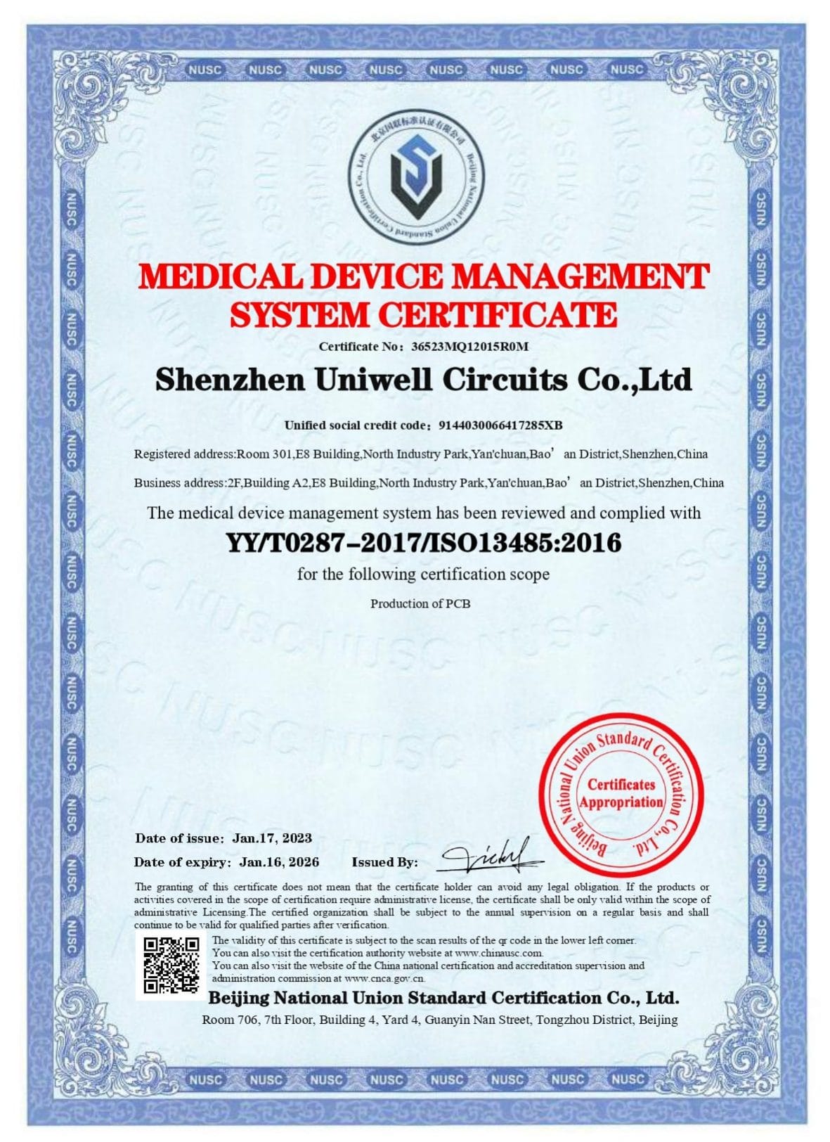
Precision Double-Sided PCB Assembly
for Compact, High-Density Electronics
Double-sided PCB assembly allows components to be mounted on both sides of your printed circuit board, doubling usable space and enabling more compact, sophisticated electronic designs. This dual-layer configuration supports compact circuit design, greater routing flexibility, and enhanced signal integrity.
- Professional SMT and through-hole assembly with comprehensive inspection
- Optimized manufacturing for both prototype and mid-volume production
- IPC-A-610 compliant processes ensuring reliable performance

ISO9001 ISO13485
ISO14001

IATF
16949

IPC-A-610H International
Certification

Fully Automated
AOI Inspection
- PCB Manufacturer
- PCB Assembly Service
- Double-Sided
Double-Sided SMT for
Complex Board Builds
Double-sided PCB assembly enables high-density electronic components to be mounted on both sides of the board using precise surface mount technology. This approach is essential for compact printed circuit board designs where space optimization, signal routing, and circuit complexity demand a double-sided layout.
SMT machines are configured to place components on one side of the PCB, followed by reflow soldering and inspection, before repeating the process on the reverse side. Double-sided SMT assembly requires reflow profile control, component weight planning, and thermal balancing across both board surfaces.
Our double-sided PCB board services include automated SMT placement down to 0201 package sizes, hand assembly for through-hole parts, and full in-line AOI, X-ray, and functional testing. We support single-sided and double-sided reflow soldering configurations with optional adhesive retention for large or bottom-facing parts. Each double-sided circuit board is manufactured in compliance with IPC-A-610 standards, with soldering process control to maintain joint quality on all sides of the board.
Our PCB assembly process supports placement of fine-pitch packages, including QFN, BGA, and CSP, with solder paste printing accuracy down to ±25 µm. During second-pass reflow soldering, we use adhesive retention for heavy components located on the bottom layers of the PCB. We also account for gravity-induced displacement by orienting heavier parts on the top side.
All double-sided PCB boards are handled with ESD-safe flipping mechanisms and vacuum conveyors to maintain alignment across both sides of the circuit board.

Our Double-Sided PCB Assembly
Capabilities
WellPCB delivers full-process double-sided PCB assembly services for advanced electronic devices. Each capability below reflects our in-house SMT precision, controlled reflow soldering, and inspection-driven workflow. From prototype to mid-volume production, we provide reliable double-sided circuit board assembly tailored to your application.
We mount components on both sides of each double-sided PCB using automated SMT systems that operate at up to 60,000 placements per hour.
Placement accuracy is maintained below ±30 µm with fiducial-based alignment that supports dual-sided mounting of 0201 passives, BGAs, QFNs, and fine-pitch ICs.
During the second pass, boards are flipped using vacuum clamping fixtures to maintain orientation and protect previously mounted devices. All placements are verified inline through SPI and post-reflow AOI.
| Specification | Value / Capability |
|---|---|
| Placement Speed | Up to 60,000 components per hour |
| Placement Accuracy | < ±30 µm (3σ, CPK ≥ 1) |
| Supported Package Types | 0201, QFN, BGA, CSP, PoP, Fine-Pitch ICs |
| Equipment Used | 8 YAMAHA + 5 Siemens SMT lines across two facilities |
| PCB Size Range | 50 mm × 50 mm to 610 mm × 508 mm |
| Minimum BGA Pitch | 0.2 mm |
| Minimum QFP Lead Width | 0.15 mm |
| Reflow Compatibility | Nitrogen oven with programmable thermal profiles |
Adhesive retention is applied selectively to components on the underside to prevent gravity-induced displacement during second-pass reflow.
We use temperature-cured red glue placed at ±0.05 mm accuracy between component leads, ensuring stability without contaminating solder pads.
For high-mass or unevenly shaped parts, this adhesive strategy enables full second-side reflow soldering without defect risk.
We apply red adhesive such as Henkel Loctite 3609, centrally positioned to avoid pad contamination, and cure it at 180 °C before the second reflow cycle begins.
We operate two separate SMT production lines to isolate lead-free and standard tin-lead assemblies.
This infrastructure allows us to process RoHS-compliant builds using SAC305 alloy in a nitrogen reflow oven while maintaining IPC-A-610 Class 2 or 3 quality benchmarks.
If required, lead-free soldering is paired with low-residue flux and pre-bake cycles to mitigate moisture sensitivity.
Clear designation of the board type ensures no material cross-contamination across double-sided PCB assembly runs.
Each side of the double-sided PCB assembly receives its own reflow cycle, optimized for the thermal demands of the component layout and copper weight.
Instead of using generic profiles, we adjust temperature ramp rates, peak hold times, and cool-down slopes to limit mechanical stress across the board.
These adjustments prevent warpage, especially on boards with large thermal gradients or asymmetrical placement. For stacked or hybrid layers, we simulate thermal response and validate each reflow soldering profile before production begins.
Nitrogen inerting is used during reflow to suppress oxidation, improving solder wetting and joint reliability across both passes. Typical profiles reach peak temperatures of 235 to 245 °C for SAC305, with soak zones maintained at 150 to 180 °C to activate flux and ensure even thermal exposure.
Inspection is integrated directly into the assembly flow, beginning with AOI after the first reflow and repeating after the second.
Our dual-camera AOI systems detect placement shifts, tombstoning, and solder bridging across both board sides. For hidden joints under BGAs or LGA packages, we use 3D X-ray imaging to identify voids, cold joints, or insufficient solder fill.
This dual-layer inspection protocol provides defect traceability for every double-sided printed circuit board we ship.
Boards that combine SMT and through-hole parts are processed with selective soldering or hand assembly, depending on layout and clearance.
Heavier connectors or legacy components are inserted post-reflow, then soldered using wave soldering or controlled heating tools. Component leads are checked for pad alignment and lead co-planarity before soldering begins.
In boards with dense via arrays, our pre-assembly checks validate annular ring clearance and copper plating continuity through the drill stack.
We offer microvias down to 3 mil diameter, blind/buried vias, and via-in-pad construction for double-sided SMT and HDI builds.
All via holes are mechanically drilled and plated using pulse electroplating to maintain wall uniformity ≥25 µm.
For stacked vias, we validate alignment through cross-section analysis and control aspect ratios up to 40:1. These structures allow high routing density without increasing board layer count.
We support full-cycle double-sided PCB board production from as few as five prototypes to orders exceeding 10,000 units.
Panel sizes range from 50 mm × 50 mm up to 610 mm × 508 mm, with finished thicknesses from 0.5 mm to 4.5 mm and copper weights up to 28 oz.
Build tracking is maintained through our MES platform, and every circuit board is verified through optical inspection and electrical test prior to packaging.
Flexible lead times allow 2 to 3 day expedited runs or standard 7 to 10-day delivery based on material availability and volume.
Our SMT lines interface with real-time MES dashboards and inline AOI/X-ray systems for closed-loop feedback and zero-defect tracking.
Data capture supports batch-level traceability, pass/fail analytics, and predictive process tuning.
Why Choose WellPCB for Your Double-Sided
PCB Assembly?

Fully Integrated Double-Sided PCB Assembly

SMT, THT, and Mixed Technology Support

Dedicated Lead-Free Processing Lines

Advanced Inspection and Testing Coverage

Fast Turnaround and Global Logistics

Process Control with Engineering Guidance
What is Double-Sided PCB Assembly?
Double-sided PCB assembly involves placing electronic components on both the top and bottom layers of a printed circuit board, increasing circuit density without expanding board size. Connections between sides are made using drilled vias and plated through holes, enabling two-sided signal routing and higher functional integration compared to single-sided designs.
The process begins with solder paste printing and surface mount component placement on the first side, followed by reflow soldering in a nitrogen oven.
Boards are then flipped, and the same sequence is repeated on the second side. Adhesives may be used to secure heavier components on the underside during reflow. Reflow profiles, copper balancing, and handling orientation are optimized to prevent displacement or warpage across both sides.
This type of PCB assembly supports SMT, through-hole, or mixed technologies, and is widely used in compact electronics, power supplies, and automotive modules requiring efficient, dual-layer circuitry.
Substrate Materials for Double-Sided PCB Boards
We support FR-4, high-Tg FR-4 (Tg >170 °C), halogen-free laminates, and ceramic-filled epoxies for enhanced thermal performance. For high-reliability builds, we recommend Isola 370HR or Shengyi S1000-2M, which offer low Z-axis expansion and better resistance to thermal cycling.
Applications with RF signal paths or impedance control requirements can be supported using Rogers RO4003C or RO4350B with dielectric constants in the 3.38 to 3.66 range and tight Dk tolerances (±0.05).
Double-Sided Assembly vs. Single-Sided SMT
| Feature | Single-Sided SMT | Double-Sided PCB Assembly |
|---|---|---|
| Component Placement | One side of the PCB only | Top and bottom sides of the board |
| Circuit Density | Limited by single-layer routing | Higher density via two-sided copper and via interconnections |
| Board Size Efficiency | Larger board needed for complex circuits | Smaller footprint for same functionality |
| Assembly Process | Single solder paste, placement, and reflow cycle | Two full SMT cycles, plus handling and second-side reflow |
| Thermal Management | Fewer heat sources, simpler cooling layout | Requires balanced component layout and controlled reflow profile |
| Component Types Supported | SMT components only | SMT, through-hole, and mixed technologies |
| Placement Equipment | JUKI RS-1 SMT line, SPI by Koh Young, AOI by Omron | Yamaha YS12F line with SPI by Cyberoptics, AOI by Test Research Inc. (TRI) |
| Use Cases | Simple electronics, low-complexity modules | Compact devices, automotive, industrial controls, consumer products |
| Cost Considerations | Lower assembly cost, fewer process steps | Slightly higher cost, offset by reduced board count per design |
Design Considerations for Double-Sided PCBs

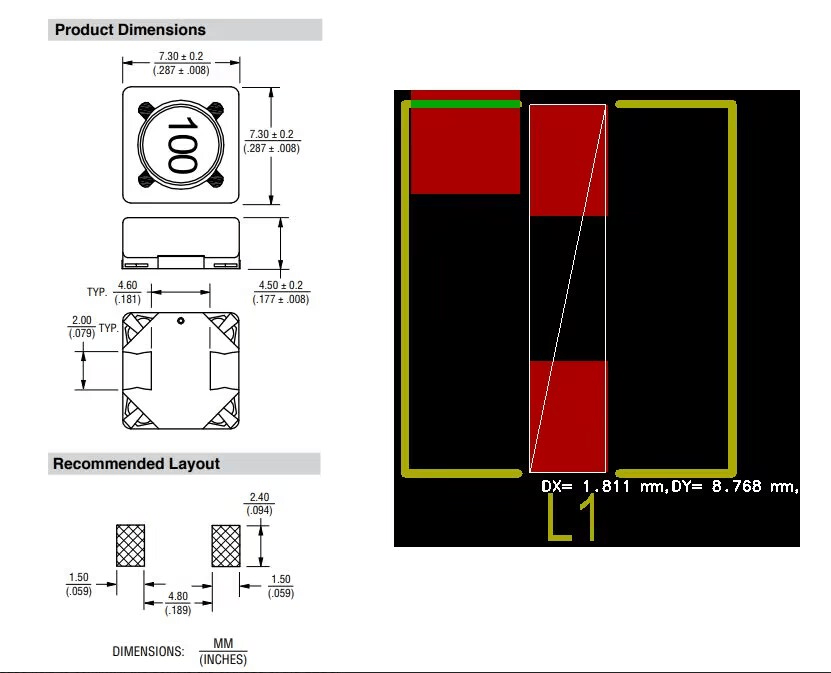
Component Weight Distribution

Thermal Profile Matching

Keep-Out Zones and Tooling Clearance

Via Design and Solder Mask Strategy

Copper Balancing

Bottom Side Adhesive Planning

DFM Rule Compliance

Thermal Management and Warpage Control
Industries We Serve with Double-Sided Assembly

Consumer Electronics
We assemble double-sided PCB boards for compact devices such as smartwatches, fitness trackers, and IoT hubs where dual-sided SMT maximizes usable board space for RF modules, sensors, and microcontrollers.

Automotive Electronics
Our assembly process supports ECUs, LED drivers, and sensor modules with dual-sided reflow, thermal balancing, and high-reliability soldering under IPC Class 3 standards for vibration and thermal cycling environments.

Medical Devices
We build double-sided printed circuit boards for portable diagnostic equipment, patient monitoring tools, and wearables. These require precise reflow soldering and optical/X-ray inspection of BGA and fine-pitch ICs.

Industrial Control Systems
WellPCB supports double-sided circuit board production for PLCs, motor drivers, and embedded controllers with through-hole and surface mount components across both board surfaces.

Telecommunications Equipment
Dual-sided assembly is used for RF front-ends, modems, and baseband boards requiring compact routing, high-speed signal integrity, and thermally optimized copper distribution.

Aerospace & Defense
We manufacture mixed-technology double-sided PCBs for avionics, radar control units, and defense-grade systems with adhesive reinforcement and 100% electrical test coverage.
How to Order Your Double-Sided
PCB Assembly in 5 Easy Steps

Submit Your PCB Design
Upload your Gerber files or use our easy online PCB design tool to create your board layout. Make sure your files are complete and correctly formatted to ensure smooth processing and production accuracy.

Select Your PCB Specifications
Customize your order by choosing the technical specifications—number of layers, board dimensions, thickness, copper weight, solder mask color, surface finish, and more. Our intuitive interface helps you configure everything based on your project’s needs.

Get an Instant Quote
Once your design and specs are in place, you'll receive a transparent, instant quote. Pricing updates in real time as you modify options, so you can adjust your selections to match your budget before placing the order.

Confirm Order & Make Payment
Review your entire order for accuracy, including file previews and selected specs. After confirmation, proceed to secure checkout and choose your preferred payment method. You’ll receive an email confirmation with order details.

Production & Delivery
Your PCB moves into production immediately. We’ll keep you updated throughout the manufacturing process. Once completed, your boards are carefully packed and shipped to your door, with tracking information provided for your convenience.
WellPCB is trusted by millions of
businesses and innovators.


Why Choose WellPCB?
WellPCB stands out among USA PCB manufacturers by delivering superior quality, advanced solutions, and unmatched reliability. With years of experience serving global markets, WellPCB has earned a reputation as one of the top PCB manufacturers in USA.
WellPCB specializes in multilayer PCBs for advanced electronic applications. You can order these boards with $100 off using our special offer, providing high complexity at competitive rates for demanding projects.


Hommer Zhao
Founder and Chief Editor – Hommer Zhao
Welcome! I’m Hommer Zhao, the founder and Chief Editor of WellPCB. With years of experience in the PCB industry, I’m committed to making sure our content is both accurate and helpful. We’re proud to serve a growing community of over 4,000 customers worldwide, and our goal is to provide you with the best resources and support. Your satisfaction is our top priority, and we’re here to help you every step of the way!

Jesse Holland
Technical Manager – Jesse Holland
Hi, I’m Jesse Holland, an Engineer and Technical Manager at WellPCB. With years of experience in PCB design and engineering, I’m here to ensure that every project we work on meets the highest technical standards. I lead our team, focusing on precision and innovation, collaborating closely with clients to provide tailored solutions and expert guidance. Whether you’re facing a complex design challenge or need advice on technical aspects, I’m here to ensure your project is a success from start to finish.

Nathan Jensen
Purchasing Manager – Nathan Jensen
Hi, I’m Nathan Jenson, the Purchasing Manager at WellPCB. I’m responsible for sourcing the best materials and components to ensure our products meet the highest quality standards. With my extensive experience in procurement, I work closely with suppliers to secure reliable and cost-effective solutions while maintaining strong relationships to support our operations. I aim to ensure every project runs smoothly by providing the resources needed to deliver on time and to your satisfaction.

Emma
Sales Manager – Emma
Hey, I am Emma, sales manager at WellPCB. I studied electronic science and technology at university and have served customers for PCB and PCB Assembly service for several years.

I enjoy communicating with customers and our technicians to solve problems, and customers always say, "It's great to have you onboard".

It is my pleasure and honour to be helpful. Contact me now, and you'll know.

Bella and Cassiel
Sales Representatives – Bella and Cassiel
We’re Bella and Cassiel, your dedicated sales representatives at WellPCB. With our extensive knowledge of the PCB industry, we’re here to provide exceptional service and support. We take the time to understand your unique needs and are always ready to offer tailored solutions and advice. Whether you need product recommendations, assistance with your orders, or simply have a question, we’re here to ensure your experience is smooth and seamless at every step.

Mandy and Wendy
Sales Representatives – Mandy and Wendy
We’re Mandy and Wendy, your friendly sales representatives at WellPCB. Passionate about helping our customers, we bring a wealth of experience in the PCB industry to provide you with the best solutions and service. We take pride in building strong relationships with our clients, understanding their specific needs, and offering personalised support to ensure their satisfaction. Whether you’re looking for advice, product information, or assistance with any part of your order, we’re here to make your experience as smooth and efficient as possible.
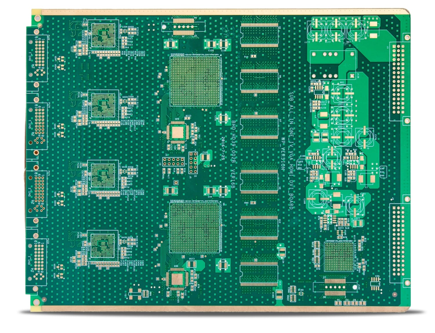
Our Team
Our skilled engineers and technicians bring expertise and precision to every PCB assembly project. Committed to quality, efficiency, and innovation, our team ensures every order meets the highest UL, IPC, ROHS & REACH standards, delivering reliable solutions tailored to your needs.
- Founder and Chief Editor – Hommer Zhao
- Technical Manager – Jesse Holland
- Purchasing Manager – Nathan Jensen
- Sales Manager – Emma
- Sales Representatives – Bella and Cassiel
- Sales Representatives – Mandy and Wendy
Double Sided PCB Assembly Case Studies

PCB Manufacturing
An electronics client needed a high-density 8-layer PCB with tight design constraints. We delivered high-performance, reliable boards meeting strict electrical and structural requirements.
PCB Specifications:
- Layers: 8
- Board Thickness: 1.8mm
- Min. Line Width/Space: 3/3.5 mil
- Min. Hole Size: 0.2mm
- Min. Distance from Hole to Line: 0.13mm
- Inner Layer Copper: Hoz
- Outer Layer Copper: 1oz
- Surface Finish: Immersion Gold
The final board met all mechanical and electrical tolerances and passed electrical testing with 100% yield. This project shows our capabilities to handle complex, high-density multilayer PCBs with tight tolerances and strict quality standards.

PCB Assembly
A PCB design firm in Italy required short-run production of a complex board with both SMT and THT components. We managed the full assembly process, including component sourcing, PCB manufacturing and assembly, inspection, and shipping.
Project Details
- Service Type: PCB Assembly
- Location: Italy
- Client Type: PCB Design Company
- Total Units: 20
- Lead Time: Rapid turnaround for prototyping
- Assembly Type: SMT+THT mixture assembly
Our experienced production team worked closely with the client to verify the BOM, optimize the stencil and the board’s layout design. We completed and delivered 20 fully assembled units within the expected lead time, allowing the client to avoid delays and meet their customers’ delivery window. This case highlights our capabilities to support global clients with flexible, low-volume PCB assembly solutions.

PCB Assembly
This PCBA solution integrates a custom PCB with high-precision SMT assembly, tailored specifically for smart fingerprint lock systems. Designed for household appliances, it combines compact size, low power consumption, and reliable signal processing to support biometric recognition and secure user access.
Technical Specifications:
- Product Type: PCBA (PCB + SMT Patch)
- Application Product: Smart Fingerprint Lock
- Industry/Application: Home Appliances / Smart Home
- Assembly Process: Surface Mount Technology (SMT)+THT
- Function: Biometric signal processing, control logic
Client Feedback On Our Double-Sided PCB Assembly
As an R&D manager, I have had an outstanding experience working with WELL-PCB. For many years, our company has entrusted them with the production, assembly, and programming of the boards developed in our R&D unit, and they have consistently exceeded our expectations.
Hamid Reza Moshayedi
R&D Manager
Their work is very impressively perfect. Today, when they check our company PCB board after assemble. They found a fake short point which many engineers has never found in the past years. But that is just designed so. The PCB board quality is excellent. Their service is also excellent.
MikeZ
My friend introduced WellPCB to me, the first try, a little look forward to. I ordered a 47*72 10ps PCB, and I can’t wait to receive my PCB. So I used expedited service and received my PCB in three days. I tested and soldered the PCB, Quality is really good, silkscreen, plating also great.
Warren Cliton
Double-Sided PCB Assembly FAQs
What is the maximum component height you support on each side of the PCB during double-sided assembly?
We support up to 25 mm component height on one side and up to 15 mm on the opposite side, depending on board thickness and fixture compatibility. Our SMT conveyors are calibrated for height asymmetry, and reflow fixtures can be customized to support uneven component profiles without causing solder joint disruption or board warpage.
Can reflow soldering be used for both sides of a double-sided PCB with large thermal mass components?
Yes, reflow soldering will be used on both sides with adjusted thermal profiles for boards containing large copper pours or high-mass packages. For the second reflow pass, we reduce ramp-up rates and extend soak times to avoid damaging first-side joints. In some cases, components on the second side are retained with red glue or mounted using hand assembly after reflow.
How do you verify solder joint quality under bottom-side BGAs or LGA components?
We use real-time 3D X-ray inspection with programmable absorption profiles to evaluate solder joint voids, bridging, and incomplete wetting under BGA and LGA packages. The imaging process captures density contrast across pad areas and internal structures, producing defect classification based on grayscale pixel analysis and structural mapping.
What adhesive types are used for bottom-side retention?
We use epoxy adhesives like Henkel Loctite 3609, applied at ±0.05 mm placement accuracy to the center body of high-mass components. These adhesives cure at 180 °C, providing mechanical retention during upside-down reflow without compromising solder paste activation or pad exposure.
What steps do you take to prevent component shift or tombstoning during second-side reflow?
Component shift is mitigated by optimized pad design, precise solder paste volume control, and gradual reflow ramp-up. Tombstoning is reduced by ensuring matched wetting forces through symmetrical pad geometry and consistent stencil aperture design. Adhesive may be selectively applied on the second side of the PCB for small passives when necessary.
Get $100 Off Your First Double-Sided PCB Assembly Order!
Streamline your next project with reliable, precision-built double-sided PCB assembly from WellPCB. Our engineers support everything from prototype builds to high-density production with dual-sided SMT, reflow profile optimization, and full optical and X-ray inspection. Submit your BOM and Gerber files today to receive expert DFM feedback, competitive pricing, and rapid global delivery.


