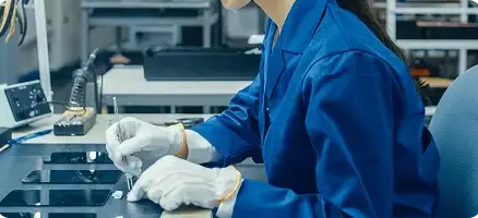
High-Frequency, Low-Loss
PTFE PCB Assembly Solutions
WellPCB provides precision PTFE PCB assembly for high-frequency applications requiring mechanical stability, low dielectric constant, chemical resistance, and tight tolerances for performance and reliability. We assemble PTFE PCBs designed for consistent signal integrity and minimal signal loss across wide temperature and frequency ranges.
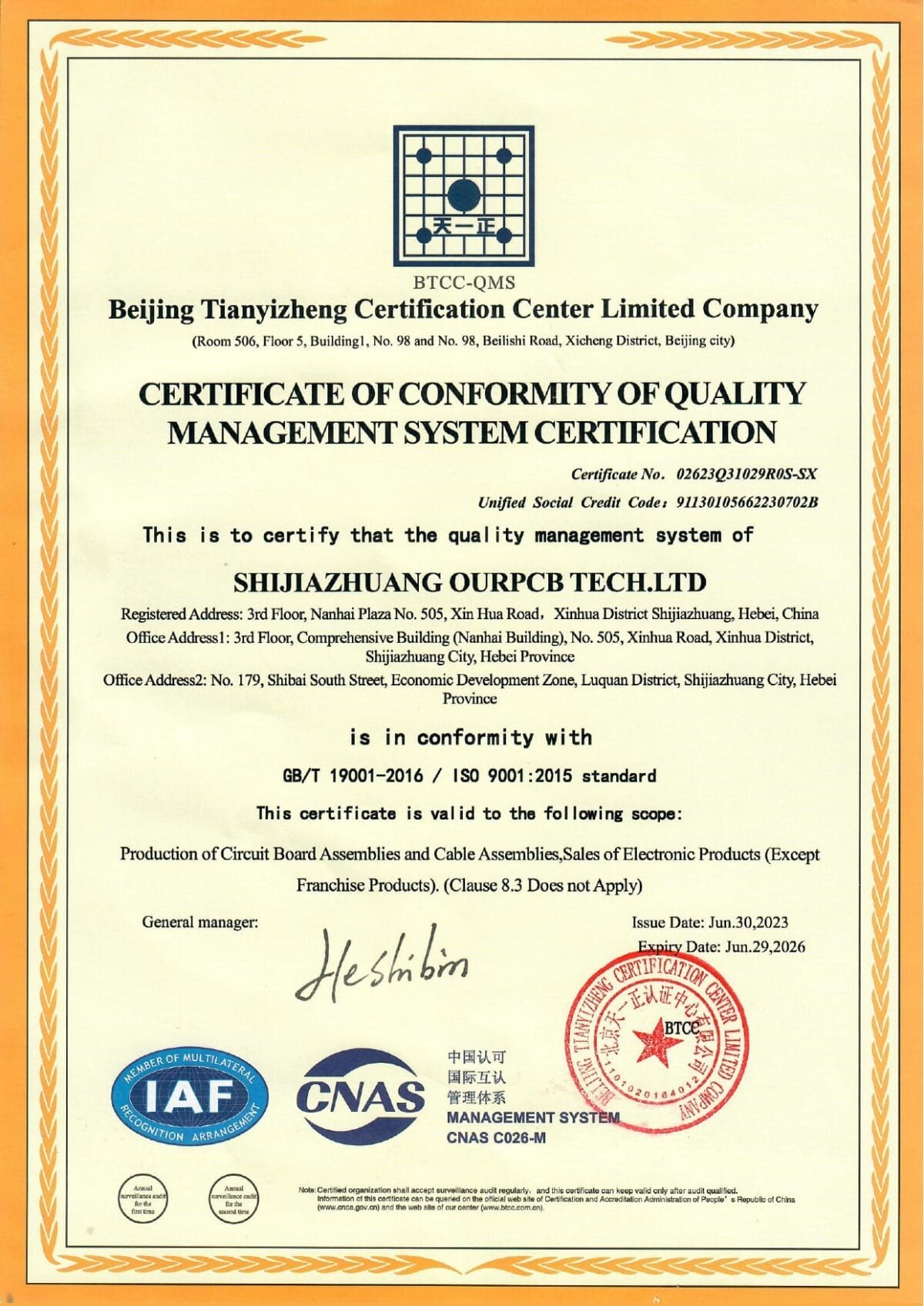
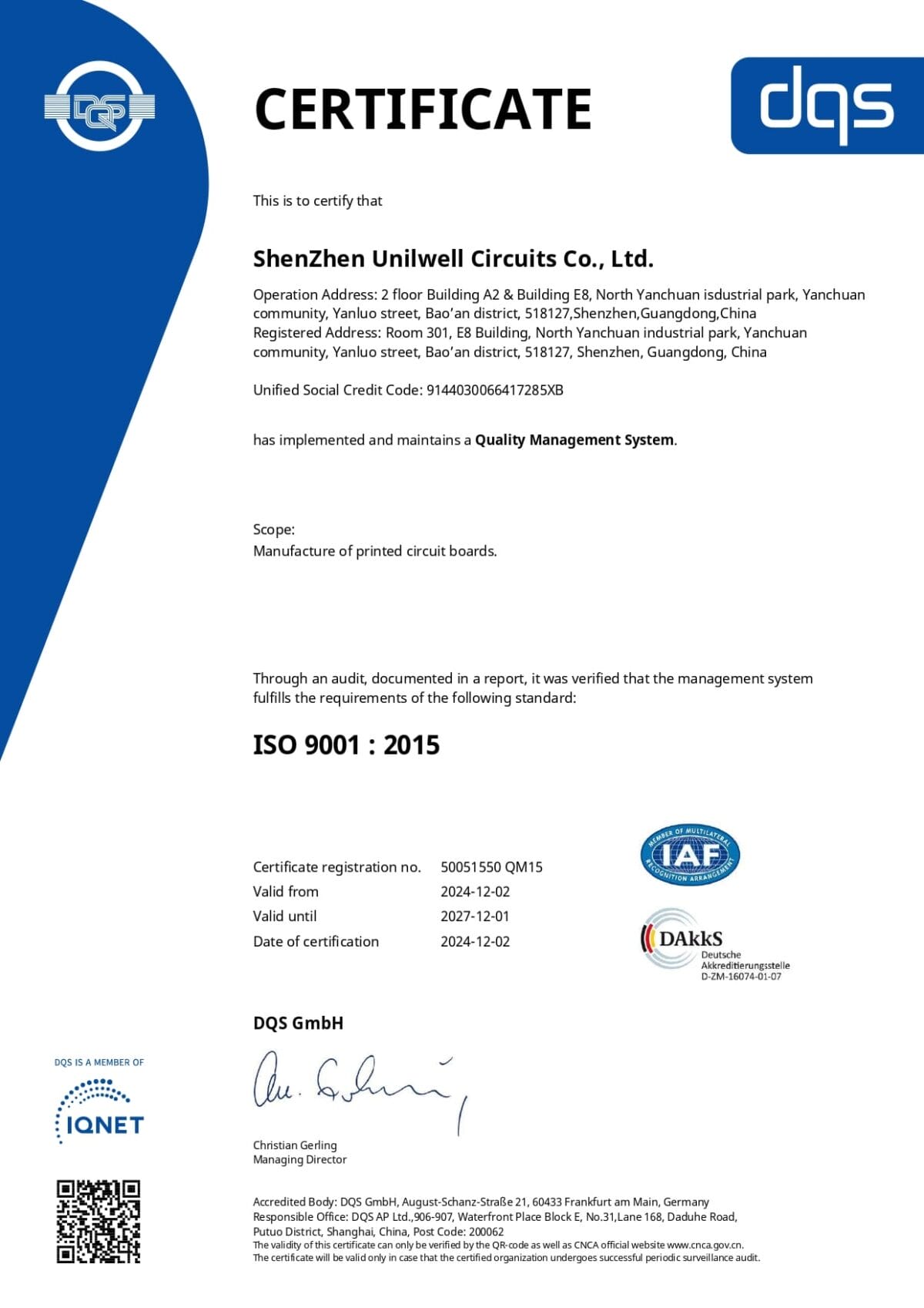
- ISO 9001, IPC-A-610 Class 3, RoHS, and Lead-Free certified PCB assembly
- Surface mount (SMT), through-hole, and mixed PCB assembly

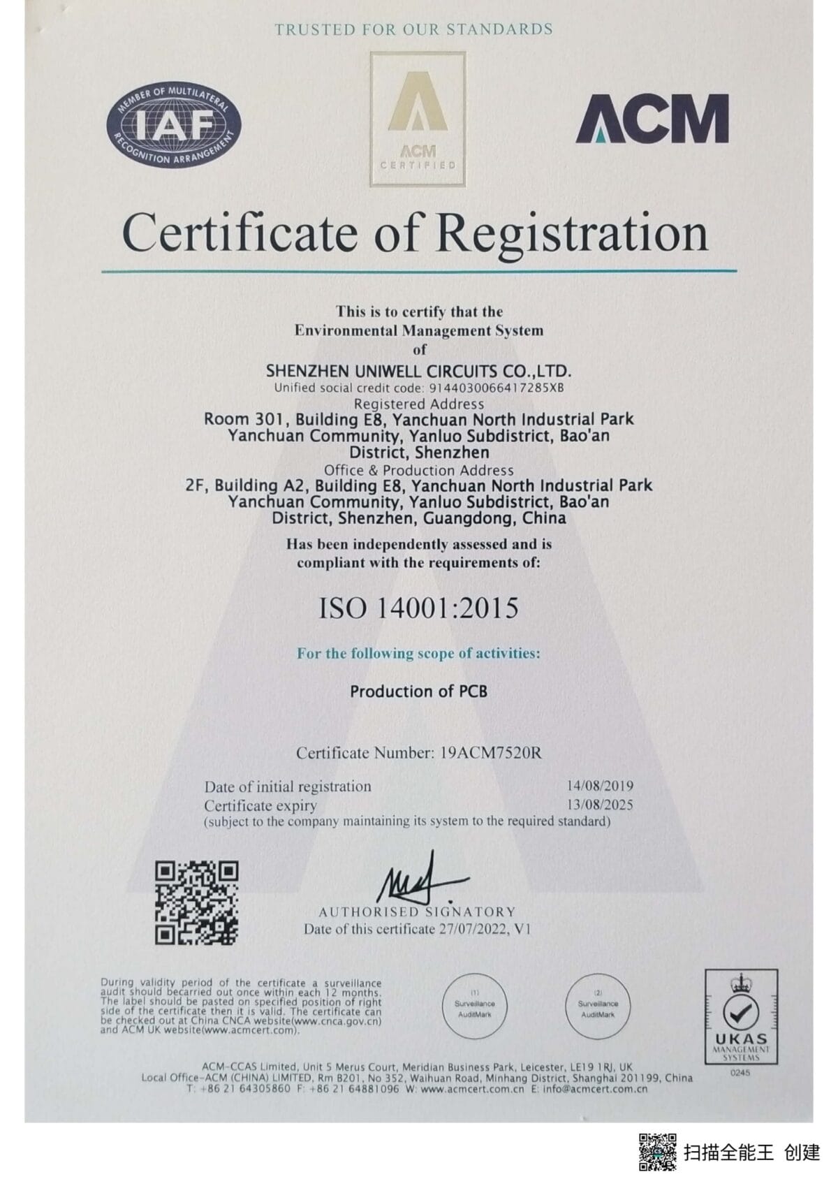
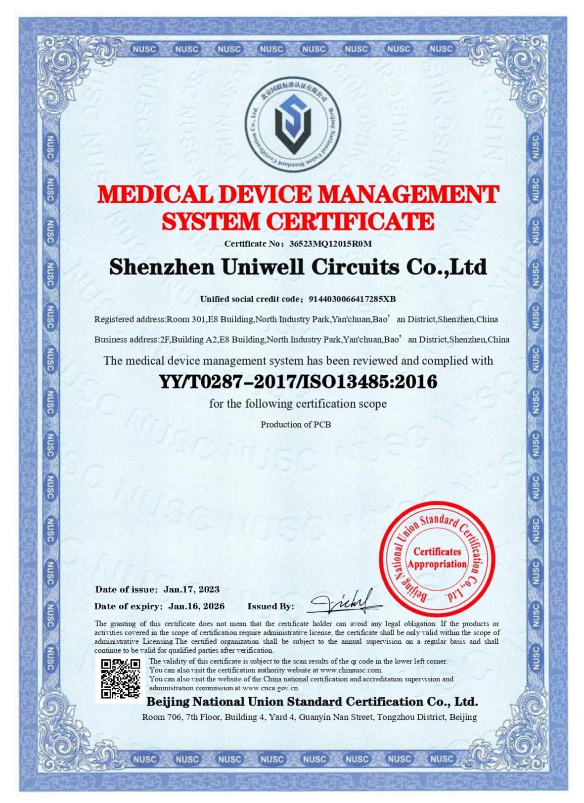
ISO9001 ISO13485
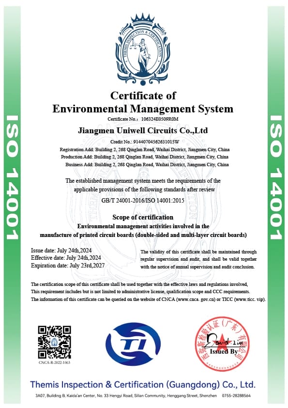
ISO14001

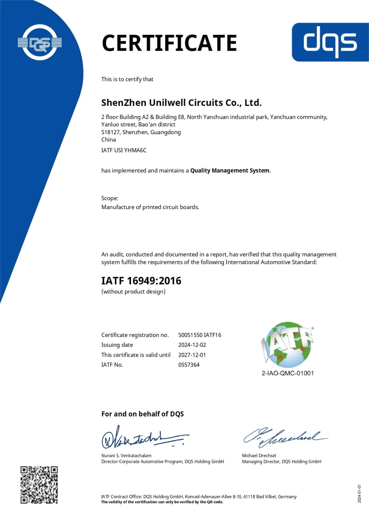
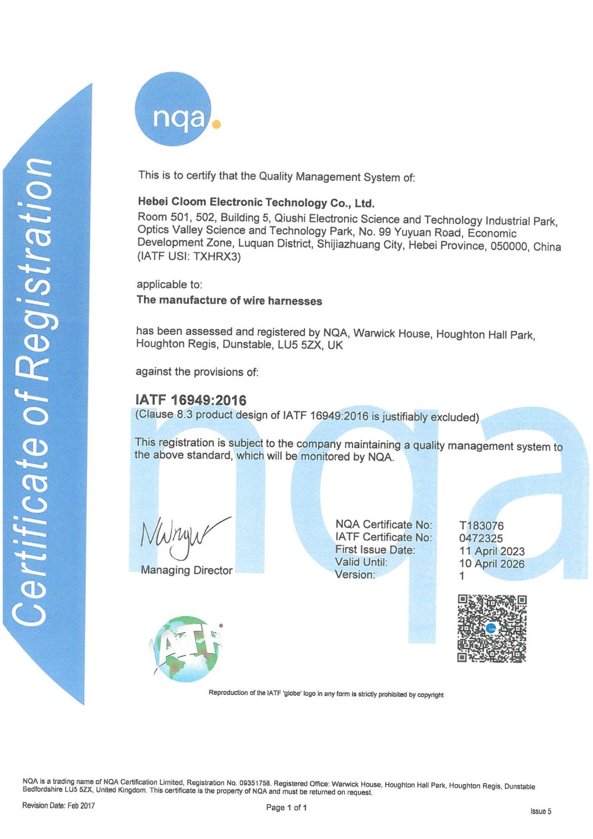
IATF
16949

IPC-A-610H International
Certification

Fully Automated
AOI Inspection
What is PTFE?
PTFE, or polytetrafluoroethylene, is a synthetic fluoropolymer used as a PCB material in high-performance PCB manufacturing and PCB assembly. Its unique electrical properties, including a low dielectric constant between 2.17 and 2.40 and a low dissipation factor below 0.0015 at 10 GHz, allow PTFE PCB substrates to maintain signal integrity and minimize signal loss in high-frequency applications.
The chemical structure of polytetrafluoroethylene or PTFE provides non-reactivity, high thermal stability, and a low coefficient of friction, making it ideal for PCB fabrication requiring stability across wide frequency ranges and temperature extremes.
PTFE offers exceptional resistance to moisture absorption, with rates typically below 0.01 percent. This protects PCB assemblies from dielectric instability and performance degradation in humid environments. The material’s coefficient of thermal expansion can reach up to 200 ppm/°C, which presents difficulties in processing but can be managed with precise assembly techniques, including controlled lamination and specialized solder processes. Our assembly processes manage PTFE’s low surface energy and high thermal expansion coefficient, reducing delamination risks and solder joint failure.
PTFE PCBs are often laminated with copper to provide stable conductor paths while preserving excellent electrical properties for RF and microwave applications. We work with leading PTFE laminates including Rogers, Taconic, Arlon, and other PTFE substrates to ensure optimal performance for your specific application requirements.
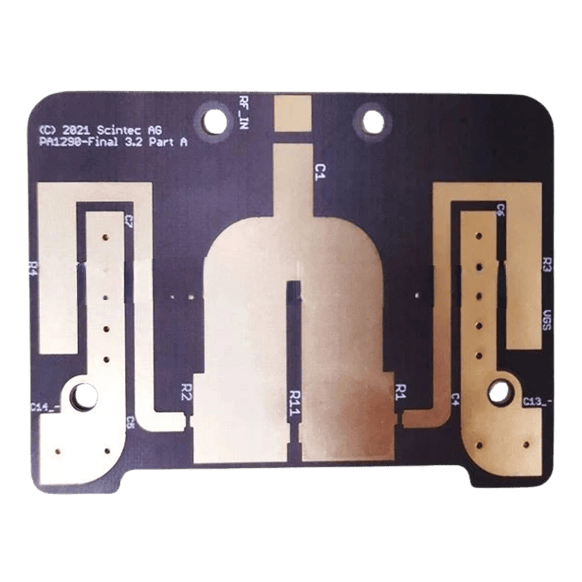
Our PTFE PCB Assembly
Capabilities
We assemble PTFE PCBs fabricated from industry-recognized laminates sourced through our partner network. Materials include Rogers RO3003, RO4350B, and RO5880, which were selected for their stable dielectric values between 2.17 and 3.48 and loss tangents ranging from 0.0009 to 0.0037 at 10 GHz.
We also work with materials from Taconic, Isola, and Arlon. This allows flexibility in meeting design specifications for various high-frequency applications and performance thresholds.
For assemblies requiring post-fabrication drilling or via rework, our processes operate at spindle speeds between 180,000 and 250,000 RPM with feed rates of 20 to 60 micrometers per revolution.
Specialized drill geometries reduce mechanical stress and prevent edge deformation. Plasma surface conditioning using argon-based treatments improves copper adhesion inside hole walls, reducing the potential for separation or via failure during reflow or field operation.
When assembling stacked or multilayer builds, we coordinate with fabrication partners to verify lamination quality. Press cycles are confirmed with temperature ranges between 260°C and 290°C and pressures from 200 to 400 psi, depending on the stack-up and resin system.
Where appropriate, we specify glass-reinforced prepregs to minimize vertical expansion and maintain mechanical alignment during assembly.
Copper feature accuracy is validated before assembly, with strict control over trace geometries to maintain impedance consistency. Etch process records confirm copper thickness tolerances within ±5% of design values, supporting signal integrity for RF and microwave circuits.
Our assembly lines use nitrogen-purged reflow ovens to limit oxidation and improve solder wetting. This method enables lower peak soldering temperatures and reduces void formation.
Plasma-treated surfaces further enhance joint reliability. We monitor solder joint integrity throughout the assembly process to prevent defects affecting high-speed or high-frequency circuits.
Completed assemblies undergo automated optical inspection (AOI) and X-ray evaluation. Electrical tests verify continuity and isolation. Where required, impedance testing, including time-domain reflectometry (TDR), is used to confirm transmission line consistency at frequencies up to 77 GHz, meeting RF performance specifications.
For builds requiring microvias or complex interconnects, we coordinate laser drilling using CO₂ or UV systems with controlled pulse energy settings. Laser parameters are selected based on laminate filler content and reinforcement to produce clean, precise vias without damaging the surrounding material.
All assembly operations comply with ISO 9001, IPC-A-610 Class 3, and RoHS directives. Assemblies designed for automotive, aerospace, or defense applications follow additional industry standards specified by customer requirements.
Where are PTFE PCBs Used?

Aerospace and Satellite Communications

RF and Microwave Systems

Medical Imaging Equipment

Industrial Sensor Networks

Automotive Radar and ADAS

High-Frequency Test Equipment
Why Choose WellPCB for Your PTFE
PCB Assembly?

Certified Quality and Process Control

Engineering Expertise in PTFE Assembly

Verified Material Sourcing

Testing to Performance Standards

Fast Quoting and Responsive Production
Features of PTFE PCBs
PTFE PCB assembly supports advanced circuit designs by combining consistent dielectric behavior with mechanical and chemical resilience. Key performance traits include:
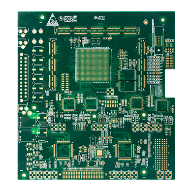

Low Dielectric Constant and Minimal Signal Loss

Dimensional Stability

Moisture Resistance and Chemical Durability

Heat Tolerance and High-Speed Compatibility
How does PTFE Compare to Other PCB Materials?
PTFE PCB assembly offers performance advantages over standard materials like FR4 and ceramic-based substrates, particularly for high-frequency applications.
| Property | PTFE | Rogers (RO4350B / RO3003) | Arlon (AD255C / CuClad) | Isola (IS620 / IS680) | Taconic (RF-35 / TLY-5A) | FR4 | Ceramic Substrates |
|---|---|---|---|---|---|---|---|
| Dielectric Constant | 2.17 – 2.40 | 3.38 (RO4350B) to 3.00 (RO3003) | 2.55 (AD255C) to 2.17 (CuClad) | 3.38 (IS680) to 3.45 (IS620) | 2.20 (RF-35) to 2.17 (TLY-5A) | 4.2 – 4.7 | 6.0 – 10.0 |
| Loss Tangent | < 0.0015 | 0.0037 (RO4350B) to 0.0010 (RO3003) | 0.0015 (AD255C) to 0.0009 (CuClad) | 0.0035 (IS680) to 0.0050 (IS620) | 0.0018 (RF-35) to 0.0011 (TLY-5A) | 0.018 – 0.025 | 0.0005 – 0.003 |
| Moisture Absorption | < 0.01% | < 0.06% | < 0.04% | < 0.10% | < 0.02% | 0.10% – 0.20% | Negligible |
| Processing Complexity | Advanced lamination and surface treatments are needed | Requires advanced lamination and surface treatments | Requires advanced lamination and surface treatments | Requires advanced lamination and surface treatments | Requires advanced lamination and surface treatments | Standard PCB fabrication | Difficult, requires specialized tooling |
| Cost Cost | Higher | Higher | Higher | Higher | Higher | Lower | Higher |
| Use in High Frequencies | Ideal for high-frequency applications | Ideal for high-frequency applications | Ideal for high-frequency applications | Ideal for high-frequency applications | Ideal for high-frequency applications | Limited by dielectric loss | Suitable but expensive |
How to Order Your PFTE PCB
in 5 Easy Steps
PCB Manufacturing and Order Review Process

Submit Your PCB Design
Upload your Gerber files or use our easy online PCB design tool to create your board layout. Make sure your files are complete and correctly formatted to ensure smooth processing and production accuracy.

Select Your PCB Specifications
Customize your order by choosing the technical specifications—number of layers, board dimensions, thickness, copper weight, solder mask color, surface finish, and more. Our intuitive interface helps you configure everything based on your project’s needs.

Get an Instant Quote
Once your design and specs are in place, you'll receive a transparent, instant quote. Pricing updates in real time as you modify options, so you can adjust your selections to match your budget before placing the order.

Confirm Order & Make Payment
Review your entire order for accuracy, including file previews and selected specs. After confirmation, proceed to secure checkout and choose your preferred payment method. You’ll receive an email confirmation with order details.

Production & Delivery
Your PCB moves into production immediately. We’ll keep you updated throughout the manufacturing process. Once completed, your boards are carefully packed and shipped to your door, with tracking information provided for your convenience.
What are the Different Types of PTFE Materials?
Selecting the right PTFE material is a key factor in optimizing PCB assembly for performance, cost, and reliability. Several PTFE laminates are available to meet the requirements of different PCB applications.

PTFE (Polytetrafluoroethylene)

Ceramic-filled PTFE

Glass-Reinforced PTFE

Ceramic Laminates (Hydrocarbon)
WellPCB is trusted by millions of
businesses and innovators.


Why Choose WellPCB?
WellPCB stands out among USA PCB manufacturers by delivering superior quality, advanced solutions, and unmatched reliability. With years of experience serving global markets, WellPCB has earned a reputation as one of the top PCB manufacturers in USA.
WellPCB specializes in multilayer PCBs for advanced electronic applications. You can order these boards with $100 off using our special offer, providing high complexity at competitive rates for demanding projects.



Hommer Zhao
Founder and Chief Editor – Hommer Zhao
Welcome! I’m Hommer Zhao, the founder and Chief Editor of WellPCB. With years of experience in the PCB industry, I’m committed to making sure our content is both accurate and helpful. We’re proud to serve a growing community of over 4,000 customers worldwide, and our goal is to provide you with the best resources and support. Your satisfaction is our top priority, and we’re here to help you every step of the way!

Jesse Holland
Technical Manager – Jesse Holland
Hi, I’m Jesse Holland, an Engineer and Technical Manager at WellPCB. With years of experience in PCB design and engineering, I’m here to ensure that every project we work on meets the highest technical standards. I lead our team, focusing on precision and innovation, collaborating closely with clients to provide tailored solutions and expert guidance. Whether you’re facing a complex design challenge or need advice on technical aspects, I’m here to ensure your project is a success from start to finish.

Nathan Jensen
Purchasing Manager – Nathan Jensen
Hi, I’m Nathan Jenson, the Purchasing Manager at WellPCB. I’m responsible for sourcing the best materials and components to ensure our products meet the highest quality standards. With my extensive experience in procurement, I work closely with suppliers to secure reliable and cost-effective solutions while maintaining strong relationships to support our operations. I aim to ensure every project runs smoothly by providing the resources needed to deliver on time and to your satisfaction.

Emma
Sales Manager – Emma
Hey, I am Emma, sales manager at WellPCB. I studied electronic science and technology at university and have served customers for PCB and PCB Assembly service for several years.
I enjoy communicating with customers and our technicians to solve problems, and customers always say, "It's great to have you onboard".
It is my pleasure and honour to be helpful. Contact me now, and you'll know.

Bella and Cassiel
Sales Representatives – Bella and Cassiel
We’re Bella and Cassiel, your dedicated sales representatives at WellPCB. With our extensive knowledge of the PCB industry, we’re here to provide exceptional service and support. We take the time to understand your unique needs and are always ready to offer tailored solutions and advice. Whether you need product recommendations, assistance with your orders, or simply have a question, we’re here to ensure your experience is smooth and seamless at every step.

Mandy and Wendy
Sales Representatives – Mandy and Wendy
We’re Mandy and Wendy, your friendly sales representatives at WellPCB. Passionate about helping our customers, we bring a wealth of experience in the PCB industry to provide you with the best solutions and service. We take pride in building strong relationships with our clients, understanding their specific needs, and offering personalised support to ensure their satisfaction. Whether you’re looking for advice, product information, or assistance with any part of your order, we’re here to make your experience as smooth and efficient as possible.
Our Team
Our skilled engineers and technicians bring expertise and precision to every PCB assembly project. Committed to quality, efficiency, and innovation, our team ensures every order meets the highest UL, IPC, ROHS & REACH standards, delivering reliable solutions tailored to your needs.
- Founder and Chief Editor – Hommer Zhao
- Technical Manager – Jesse Holland
- Purchasing Manager – Nathan Jensen
- Sales Manager – Emma
- Sales Representatives – Bella and Cassiel
- Sales Representatives – Mandy and Wendy
Case Studies
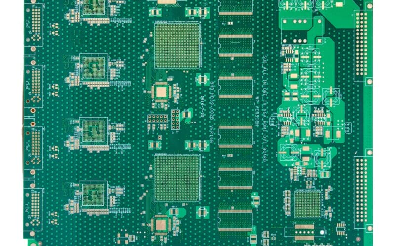
PCB Manufacturing
PCB Specifications
- Layers: 8
- Board Thickness: 1.8mm
- Min. Line Width/Space: 3/3.5 mil
- Min. Hole Size: 0.2mm
- Min. Distance from Hole to Line: 0.13mm
- Inner Layer Copper: Hoz
- Outer Layer Copper: 1oz
- Surface Finish: Immersion Gold
The final board met all mechanical and electrical tolerances and passed electrical testing with 100% yield. This project shows our capabilities to handle complex, high-density multilayer PCBs with tight tolerances and strict quality standards.
PCB Assembly
Project Details
- Service Type: PCB Assembly
- Location: Italy
- Client Type: PCB Design Company
- Total Units: 20
- Lead Time: Rapid turnaround for prototyping
- Assembly Type: SMT+THT mixture assembly
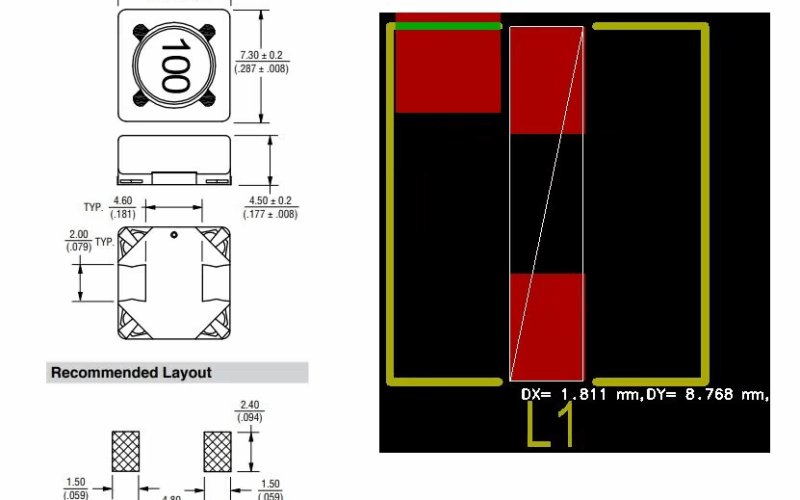
Our experienced production team worked closely with the client to verify the BOM, optimize the stencil and the board’s layout design. We completed and delivered 20 fully assembled units within the expected lead time, allowing the client to avoid delays and meet their customers’ delivery window. This case highlights our capabilities to support global clients with flexible, low-volume PCB assembly solutions.
Wire Harness
Project Details
- Service Type: Custom Automotive Wire Harness
- Location: New York, USA
- Client Type: Auto Repair Shop
- Quantity: 10,000 Units
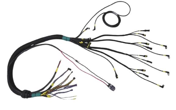
Our team followed strict quality guidelines throughout production, using automotive-grade connectors and insulation materials. The order was completed on schedule with no reported defects, supporting the client’s rollout without interruption. This case shows our comprehensive capabilities in large-scale production, customized solutions, quality control and efficient delivery.
PFTE PCB Service: Client Feedback
As an R&D manager, I have had an outstanding experience working with WELL-PCB. For many years, our company has entrusted them with the production, assembly, and programming of the boards developed in our R&D unit, and they have consistently exceeded our expectations.
Hamid Reza Moshayedi
R&D Manager
Their work is very impressively perfect. Today, when they check our company PCB board after assemble. They found a fake short point which many engineers has never found in the past years. But that is just designed so. The PCB board quality is excellent. Their service is also excellent.
MikeZ
My friend introduced WellPCB to me, the first try, a little look forward to. I ordered a 47*72 10ps PCB, and I can’t wait to receive my PCB. So I used expedited service and received my PCB in three days. I tested and soldered the PCB, Quality is really good, silkscreen, plating also great.
Warren Cliton
Teflon PCB Fabricator | FAQs
What design considerations apply to PTFE PCB assembly?
Designers should consider material handling challenges, including adhesion properties and dimensional control. Clearances, pad sizes, and via structures must accommodate potential movement during soldering and assembly.
What are the benefits of using PTFE for circuit assemblies?
PTFE PCBs offer a low dielectric constant and minimal signal loss, supporting high-frequency applications where impedance stability and reduced phase distortion are important.
How does PTFE material affect soldering processes?
PTFE surfaces require plasma treatment or chemical conditioning to improve solder adhesion. Soldering in nitrogen environments reduces oxidation and promotes reliable joint formation without excessive thermal stress.
What are common PTFE PCB assembly problems, and how are they addressed?
PTFE assemblies can face adhesion issues due to the material’s low surface energy, leading to pad separation or poor solder joint formation. Plasma surface treatments are applied to increase wettability before assembly.
Via deformation and drilling burrs may occur because of the material’s softness and elasticity; these are controlled by using high-RPM drilling with optimized chip loads and post-drill cleaning. During reflow, dimensional movement can cause trace misalignment. This is managed through controlled temperature ramp rates, fixture support, and reinforced laminate selection when appropriate.
When was PTFE Discovered?
Polytetrafluoroethylene (PTFE) was discovered in 1938 by Dr. Roy J. Plunkett during experiments with tetrafluoroethylene gas. The accidental polymerization produced a solid material with a low dielectric constant, high thermal stability, and strong chemical resistance.
These properties, combined with its low coefficient of friction, led to the development of PTFE material for electrical insulation and, eventually, for PCB substrates in RF and microwave systems.
By the 1950s, the use of Teflon expanded into high-frequency transmission lines and advanced circuit boards. The ability of PTFE PCBs to support consistent electrical properties across a wide frequency range made them suitable for demanding high-frequency applications.
Over time, processing techniques evolved to address difficulties in processing, including adhesion challenges and managing the coefficient of thermal expansion during PCB fabrication and PCB assembly. Today, Teflon PCB materials remain a standard for high-frequency circuits requiring stable performance in extreme conditions.
Work with WellPCB: Your Trusted PTFE PCB Assembly Partner
