Precision Quick Turn PCB Fabrication and
Assembly for Prototypes and Production
Quick turn PCBs are manufactured using compressed lead times, with fabrication completed in as little as 24 hours for standard multilayer builds. WellPCB operates two certified PCB fabrication plants and two PCB assembly facilities capable of handling multi-layer rigid, flexible, and rigid-flex quick turn printed circuit boards.
- 24 to 48 hour quick turn PCB fabrication for rapid prototyping and production
- Quick turn prototyping with integrated DFM analysis and design optimization
- Fast turn circuit board assembly with advanced component placement capabilities

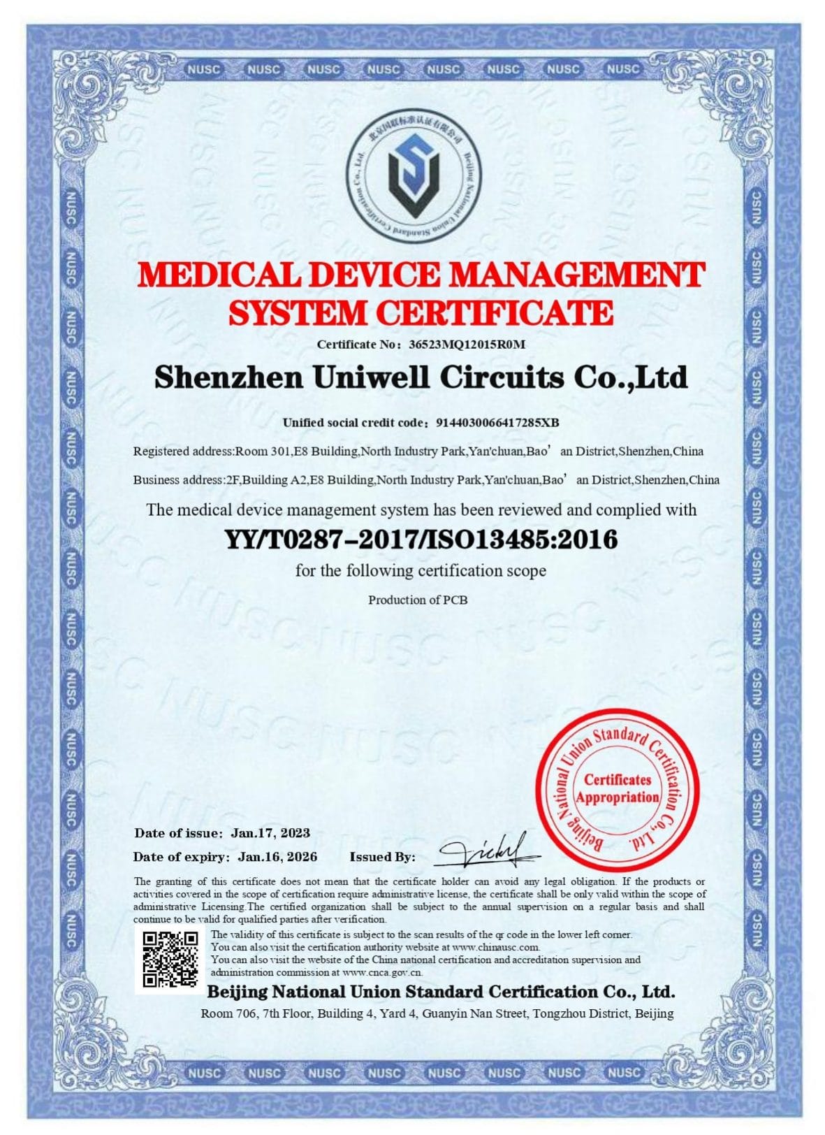
ISO9001 ISO13485
ISO14001

IATF
16949

IPC-A-610H International
Certification

Fully Automated
AOI Inspection
- PCB Manufacturer
- PCB Assembly Service
- Quick Turn
Fast PCB Prototyping and Express Production for Time-Sensitive Projects
Quick turn PCB fabrication eliminates the delays associated with traditional board manufacturing by combining high-speed CAM processing, accelerated solder mask exposure, and fast turn panel preparation. WellPCB uses parallelized processes for stencil creation, BOM validation, and copper pattern imaging to reduce turnaround times for all quick turn PCB fabrication orders.
Our fast PCB prototyping service supports builds from 1 to 64 layers using FR4, Rogers, and halogen-free substrates, with lead times starting at 72 hours for 1-12 layer PCBs. Board builds support minimum trace width of 1.8 mil, mechanical drill diameters down to 0.08 mm, and copper weights from 0.33 to 28 oz. Our solder mask layer processing includes green, white, black, and matte options for ENIG, HASL, OSP, or Immersion Silver finishes.
Fast turn circuit board assembly capabilities include BGA, QFP, and micro-SMT components down to 0.2 mm pitch, with specialized handling for high-density layouts. Quick turn fabrication utilizes FR4, High Tg FR4, and hybrid stackups optimized for accelerated processing, while CAM-based DFM edits ensure ViewMate compatibility for seamless file processing.
Each quick turn printed circuit board is verified through AOI and electrical testing, with optional X-ray for complex via structures such as blind, buried, and via-in-pad configurations. Turnkey projects benefit from integrated Gerber file review, component kitting, and solder paste stencil alignment before board assembly.
Whether you need a PCB quick turn for pre-production validation, rapid turnaround PCB samples for customer demos, or fast turn PCB assembly for a time-sensitive launch, our system is built to compress cycle time without compromising trace definition, surface finish quality, or plating uniformity.

Our Quick Turn PCB Capabilities
Our quick turn PCB services are built on a high-speed, high-precision workflow that supports a wide range of PCB types, finishes, and feature densities. We use in-house tooling, automated optical inspection, and rapid DFM correction to reduce processing delays.
Every quick turn PCB fabrication project is run on a parallelized schedule with test integration, fast solder mask exposure, and IPC Class 2 or Class 3 inspection procedures.
We fabricate quick turn printed circuit boards with 1 to 32 layers, offering 24-hour turnaround for 2 to 6-layer FR4 builds and 3 to 5-day turnaround for 8 to 12 layer designs.
Stackups can include symmetrical, HDI, and hybrid configurations using standard prepreg or high-Tg core laminates.
All builds follow IPC-6012 standards and are panelized using customer-defined arrays or V-score outlines. This impacts lead time because every added layer increases imaging, registration, and lamination steps.
| Layer Count | Typical Turnaround Time |
|---|---|
| 1 to 2 Layers | 24 to 48 hours |
| 4 to 6 Layers | 24 to 72 hours |
| 8 to 12 Layers | 3 to 5 days |
| 14 to 64 Layers | 5 to 10 days |
Minimum trace width and spacing for fast turn PCB fabrication is 1.8 mil using LDI (laser direct imaging) technology.
Controlled impedance is supported for differential pairs and single-ended signals, with trace width matching tolerances within ±10% for specified dielectric stacks.
Annular rings are held to a minimum of 0.006 in for reliable via formation on dense signal layers.
Quick turn PCB fab services support standard FR4 (Tg135), mid-grade high-Tg FR4 (Tg170), and premium Tg180 substrates for thermal stability.
Rogers materials can be integrated on request for RF and high-speed builds. All boards are UL 94V-0 rated and RoHS compliant.
Rigid-flex boards use polyimide flex layers with adhesive or adhesiveless constructions down to 0.05 mm flex thickness.
We offer quick turn PCB fabrication with finished copper weights ranging from 0.33 oz to 28 oz for internal layers, and up to 28 oz for external layers.
These support high-current and thermal dissipation needs in automotive and power supply applications. Final board thickness ranges from 0.1 mm to 12 mm, with dielectric thickness controlled to within ±10%.
All copper thicknesses are plated to IPC Class 2 or Class 3 standards, depending on application requirements.
Our fast turn PCB options include ENIG, lead-free HASL, leaded HASL, Immersion Silver, and OSP surface finishes. HASL finishes are processed within 20 to 30 minutes, while ENIG cycles range from 90 to 120 minutes depending on plating thickness.
Selective plating combinations, such as ENIG with hard gold edge connectors, are available for production services with slightly extended lead times.
Finish selection is optimized during DFM to match solderability and environmental compliance goals. This matters because ENIG and HASL have different processing times that affect same-day or 48-hour delivery windows.
All quick turn PCB orders include electrical testing and AOI verification at no additional cost. AOI scanning is performed on both outer and inner layers where applicable, using high-resolution optics calibrated to detect minimum feature violations down to 3 mil.
Functional circuit testing and X-ray inspection are available for fast PCB assembly orders involving BGAs or bottom-terminated packages.
Finished boards include optional UL markings, 94V-0 certification, and RoHS-compliant lead-free labeling.
Quick turn PCB assembly services are supported with SMT stencil generation, BOM sourcing from authorized distributors, and solder paste file generation directly from the Gerber layer stack.
Assembly options include 0201 package placement, 0.2 mm pitch QFN and BGA, and single or double-sided population. Assembly lead time adds 1 to 2 days, depending on part availability and stencil configuration.
Each assembled board passes visual inspection, solder joint analysis, and functional test (optional).
Every quick turn PCB project begins with a full CAM-level design for manufacturability (DFM) review using ViewMate and internal Gerber analysis tools.
We automatically correct common issues including solder mask swell, annular ring violations, and silkscreen legibility conflicts.
All files must be submitted in Gerber RS-274X or 274D format, with Excellon drill files, BOM, and assembly notes included in a single ZIP archive.
Our engineers validate minimum trace width, via sizes, stackup integrity, and plating callouts before releasing the job to fabrication.
For fast turn circuit board assembly, we confirm MPN matching and perform kitting checks prior to stencil alignment.
All quick turn printed circuit boards are built to IPC-6012 Class 2 or Class 3 requirements.
Visual inspection follows IPC-A-600 protocols, and all boards use UL 94V-0 certified laminates. RoHS compliance is supported for both leaded and lead-free solder profiles.
Why Choose WellPCB for Your Quick Turn
PCB Manufacturing?

24-Hour Quick Turn PCB Fab for Rigid and HDI Builds

Turnkey Quick Turn PCB Assembly Services

Fully Integrated Fabrication and Assembly Workflow

Automated DFM Error Correction and Pre-Flight Checks

Certified Quick Turnaround PCB Builds for Regulated Markets

No MOQ, Live Quotes, and Same-Day Engineering
Review
What is Quick Turn PCB Manufacturing?
Quick turn PCB manufacturing compresses the full PCB production cycle into 1 to 7 days by parallelizing fabrication and assembly tasks. It begins with Gerber and Excellon file submission, followed by automated DFM checks that correct solder mask swell, annular ring violations, and drill mismatches.
Standard quick turn PCB fabrication supports 2 to 6 layer FR4 boards in 24 to 48 hours, using 1.8 mil trace widths, 0.08 mm via drills, and 0.1 to 12 mm finished thickness. HDI and multi-layer PCB designs follow a 3 to 5 day cycle with sequential lamination. Available finishes include ENIG, HASL, Immersion Silver, and OSP.
Quick turn PCB assembly services begin within 24 hours of fabrication using synchronized stencil and BOM data. SMT lines support 0.2 mm BGA pitch, RoHS lead-free profiles, and are verified by AOI, probe test, and X-ray for high-reliability applications.
Industries that Use Our Quick Turn PCB Services

Medical Devices

Consumer Electronics

Automotive Systems
Used in EV battery controllers, ADAS, infotainment units, and ECU subsystems.
Quick turn PCB fab services support Class 3 reliability, controlled impedance, and via-in-pad for high-density layouts.

Aerospace & Defense

IoT & Industrial Control
Used in sensor hubs, smart meters, and embedded controllers.
Quickturn PCBs for industrial clients support BGA, QFN, and multi-board panelization with fast turn circuit board assembly.

Academic & Research Labs
What’s the Difference Between Quick Turn
vs Traditional Manufacturing?
| Feature | Quick Turn PCB Manufacturing | Traditional PCB Manufacturing |
|---|---|---|
| Turnaround Time | 24 to 72 hours for 2 to 12 layer FR4 builds | 2 to 5 weeks, depending on queue and stack complexity |
| Layer Count Support | Up to 12 layers standard, 64 layers with expedited quote | Up to 32 layers with longer fabrication cycles |
| Surface Finish Timing | HASL in 30 minutes, ENIG in 90 to 120 minutes | Same finishes with delayed access to plating lines |
| Minimum Order Quantity | No MOQ; start with 1 custom PCB prototype | Commonly 25 to 100 unit minimums for low-tier orders |
| Design Flexibility | Accepts last-minute changes with real-time DFM correction | File revisions delay the entire production queue |
| Via and Trace Capabilities | 0.08 mm via drills, 1.8 mil trace/space, controlled impedance on request | Same specs available, but longer tooling lead time |
| Certifications | IPC-6012, RoHS, Class 2/3, UL 94V-0 ready within quick turn timeframe | Same certifications, longer audit and QA cycle |
| Use Case Fit | Rapid PCB prototyping, urgent deployment, fast turn custom PCB builds | Volume production with slower delivery and lower cost per unit |
What Design Considerations Should You Know
for Quick Turn PCB Manufacturing?
| Design Factor | Technical Consideration |
|---|---|
| DFM Compliance | Submit clean Gerber files with solder mask layer, drill chart, and copper layer alignment. CAM tools will flag unsupported traces, mask clearance issues, or annular ring violations. |
| Stackup Simplicity | Use symmetrical stackups with no more than two lamination cycles to maintain 3 to 5 day quick turnaround PCB schedules. |
| Via Design | Avoid via-in-pad unless necessary. Filled and plated-over vias add 1 to 2 days to fast turn PCB fabrication. Blind and buried vias are accepted with clear drill layer maps. |
| Surface Finish Selection | Choose ENIG or HASL for fast processing. Mixed finishes (ENIG + hard gold) are not recommended for quick turn PCB fab. |
| Material Choice | Use in-stock FR4 (Tg135 to Tg180) or halogen-free cores. Non-standard substrates may increase lead time. |
| Component Availability | Select commonly stocked parts for quick turn PCB assembly services. Validate MPNs with authorized suppliers like Digi-Key or Mouser. |
| File Submission Format | Compress Gerber files, Excellon drills, BOM, centroid file, and assembly notes into a single ZIP. Label each file layer clearly. |
| Silkscreen and Labels | Maintain silkscreen clearance from pads and vias. Use 0.15 mm minimum line width and avoid overlapping polarity markings. |
How to Order Your Quick Turn
PCB in 5 Easy Steps

Submit Your PCB Design
Upload your Gerber files or use our easy online PCB design tool to create your board layout. Make sure your files are complete and correctly formatted to ensure smooth processing and production accuracy.

Select Your PCB Specifications
Customize your order by choosing the technical specifications—number of layers, board dimensions, thickness, copper weight, solder mask color, surface finish, and more. Our intuitive interface helps you configure everything based on your project’s needs.

Get an Instant Quote
Once your design and specs are in place, you'll receive a transparent, instant quote. Pricing updates in real time as you modify options, so you can adjust your selections to match your budget before placing the order.

Confirm Order & Make Payment
Review your entire order for accuracy, including file previews and selected specs. After confirmation, proceed to secure checkout and choose your preferred payment method. You’ll receive an email confirmation with order details.

Production & Delivery
Your PCB moves into production immediately. We’ll keep you updated throughout the manufacturing process. Once completed, your boards are carefully packed and shipped to your door, with tracking information provided for your convenience.
WellPCB is trusted by millions of
businesses and innovators.


Why Choose WellPCB?
WellPCB stands out among USA PCB manufacturers by delivering superior quality, advanced solutions, and unmatched reliability. With years of experience serving global markets, WellPCB has earned a reputation as one of the top PCB manufacturers in USA.
WellPCB specializes in multilayer PCBs for advanced electronic applications. You can order these boards with $100 off using our special offer, providing high complexity at competitive rates for demanding projects.




Hommer Zhao
Founder and Chief Editor – Hommer Zhao
Welcome! I’m Hommer Zhao, the founder and Chief Editor of WellPCB. With years of experience in the PCB industry, I’m committed to making sure our content is both accurate and helpful. We’re proud to serve a growing community of over 4,000 customers worldwide, and our goal is to provide you with the best resources and support. Your satisfaction is our top priority, and we’re here to help you every step of the way!

Jesse Holland
Technical Manager – Jesse Holland
Hi, I’m Jesse Holland, an Engineer and Technical Manager at WellPCB. With years of experience in PCB design and engineering, I’m here to ensure that every project we work on meets the highest technical standards. I lead our team, focusing on precision and innovation, collaborating closely with clients to provide tailored solutions and expert guidance. Whether you’re facing a complex design challenge or need advice on technical aspects, I’m here to ensure your project is a success from start to finish.

Nathan Jensen
Purchasing Manager – Nathan Jensen
Hi, I’m Nathan Jenson, the Purchasing Manager at WellPCB. I’m responsible for sourcing the best materials and components to ensure our products meet the highest quality standards. With my extensive experience in procurement, I work closely with suppliers to secure reliable and cost-effective solutions while maintaining strong relationships to support our operations. I aim to ensure every project runs smoothly by providing the resources needed to deliver on time and to your satisfaction.

Emma
Sales Manager – Emma
Hey, I am Emma, sales manager at WellPCB. I studied electronic science and technology at university and have served customers for PCB and PCB Assembly service for several years.
I enjoy communicating with customers and our technicians to solve problems, and customers always say, "It's great to have you onboard".
It is my pleasure and honour to be helpful. Contact me now, and you'll know.

Bella and Cassiel
Sales Representatives – Bella and Cassiel
We’re Bella and Cassiel, your dedicated sales representatives at WellPCB. With our extensive knowledge of the PCB industry, we’re here to provide exceptional service and support. We take the time to understand your unique needs and are always ready to offer tailored solutions and advice. Whether you need product recommendations, assistance with your orders, or simply have a question, we’re here to ensure your experience is smooth and seamless at every step.

Mandy and Wendy
Sales Representatives – Mandy and Wendy
We’re Mandy and Wendy, your friendly sales representatives at WellPCB. Passionate about helping our customers, we bring a wealth of experience in the PCB industry to provide you with the best solutions and service. We take pride in building strong relationships with our clients, understanding their specific needs, and offering personalised support to ensure their satisfaction. Whether you’re looking for advice, product information, or assistance with any part of your order, we’re here to make your experience as smooth and efficient as possible.
Our Team
Our skilled engineers and technicians bring expertise and precision to every PCB assembly project. Committed to quality, efficiency, and innovation, our team ensures every order meets the highest UL, IPC, ROHS & REACH standards, delivering reliable solutions tailored to your needs.
- Founder and Chief Editor – Hommer Zhao
- Technical Manager – Jesse Holland
- Purchasing Manager – Nathan Jensen
- Sales Manager – Emma
- Sales Representatives – Bella and Cassiel
- Sales Representatives – Mandy and Wendy
Quick Turn PCB Case Studies
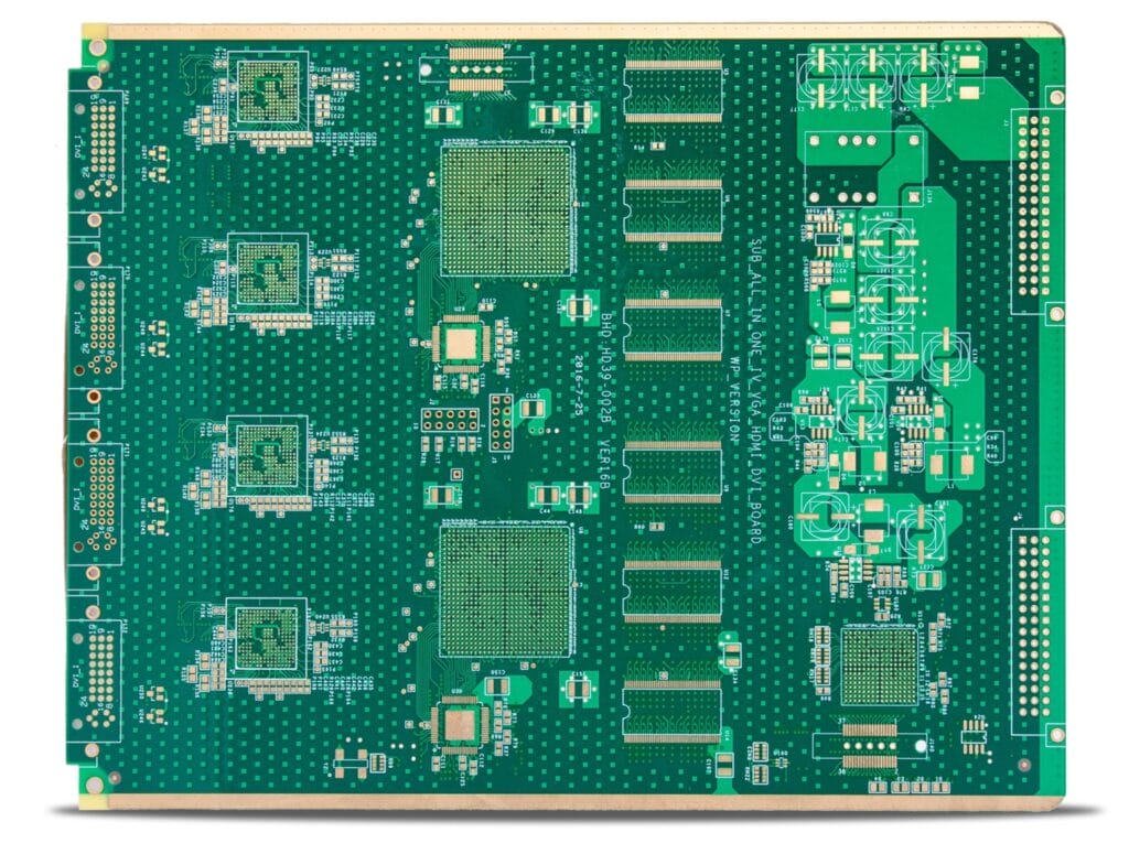
PCB Manufacturing
An electronics client needed a high-density 8-layer PCB with tight design constraints. We delivered high-performance, reliable boards meeting strict electrical and structural requirements.
PCB Specifications:
- Layers: 8
- Board Thickness: 1.8mm
- Min. Line Width/Space: 3/3.5 mil
- Min. Hole Size: 0.2mm
- Min. Distance from Hole to Line: 0.13mm
- Inner Layer Copper: Hoz
- Outer Layer Copper: 1oz
- Surface Finish: Immersion Gold
The final board met all mechanical and electrical tolerances and passed electrical testing with 100% yield. This project shows our capabilities to handle complex, high-density multilayer PCBs with tight tolerances and strict quality standards.
PCB Assembly
A PCB design firm in Italy required short-run production of a complex board with both SMT and THT components. We managed the full assembly process, including component sourcing, PCB manufacturing and assembly, inspection, and shipping.
Project Details
- Service Type: PCB Assembly
- Location: Italy
- Client Type: PCB Design Company
- Total Units: 20
- Lead Time: Rapid turnaround for prototyping
- Assembly Type: SMT+THT mixture assembly
Our experienced production team worked closely with the client to verify the BOM, optimize the stencil and the board’s layout design. We completed and delivered 20 fully assembled units within the expected lead time, allowing the client to avoid delays and meet their customers’ delivery window. This case highlights our capabilities to support global clients with flexible, low-volume PCB assembly solutions.
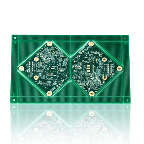
PCB Assembly
This 4-layer Quick Turn High TG PCB is engineered for rapid production cycles without compromising on thermal stability and reliability. Designed to meet IPC Class III standards, it is ideal for high-reliability applications such as industrial control, aerospace, and medical electronics.
Technical Specifications:
- Layer Count: 4 Layers
- Board Thickness: 1.57 mm
- Material: FR4 TG150
- Surface Finish: Immersion Gold (ENIG)
- Line Width / Spacing: 8 mil / 6 mil
- Special Requirement: IPC Class III Compliance
- Quick Turn Production: 24–72 hours lead time
Our Quick Turn PCB Client Feedback
As an R&D manager, I have had an outstanding experience working with WELL-PCB. For many years, our company has entrusted them with the production, assembly, and programming of the boards developed in our R&D unit, and they have consistently exceeded our expectations.
Hamid Reza Moshayedi
R&D Manager
Their work is very impressively perfect. Today, when they check our company PCB board after assemble. They found a fake short point which many engineers has never found in the past years. But that is just designed so. The PCB board quality is excellent. Their service is also excellent.
MikeZ
My friend introduced WellPCB to me, the first try, a little look forward to. I ordered a 47*72 10ps PCB, and I can’t wait to receive my PCB. So I used expedited service and received my PCB in three days. I tested and soldered the PCB, Quality is really good, silkscreen, plating also great.
Warren Cliton
Quick Turn PCB FAQs
Can you support quick turn PCB assembly with BGA or QFN components?
Yes, our fast PCB assembly service supports 0.2 mm BGA pitch, 0.15 mm QFN, and 0201 passives. Assembly begins within 24 hours of fabrication and includes AOI, probe test, and optional X-ray inspection for high-density layouts.
What file formats are required for quick turn PCB fabrication?
Submit Gerber RS-274X or 274D files, Excellon2 NC drill files, and a drill tool list. For quick turn PCB assembly, include BOM, pick-and-place file, and labeled centroid data in a single ZIP archive.
Can you handle impedance-controlled quickturn PCBs with via-in-pad?
Yes, but via-in-pad requires filled and plated-over processing, which adds 1 to 2 days. We support impedance targets of ±10% with trace widths down to 1.8 mil and copper weights up to 28 oz for outer layers.
Get $100 Off Your First Quick Turn PCB Order
WellPCB delivers fast turn custom PCB fabrication and assembly services with 24 to 72 hour lead times, full DFM validation, and IPC Class 3 certified quality. Whether you need rapid PCB prototyping, turnkey quick turn PCB assembly services, or HDI quick turnaround PCB builds, we help you meet deadlines without compromising technical accuracy or production standards.
