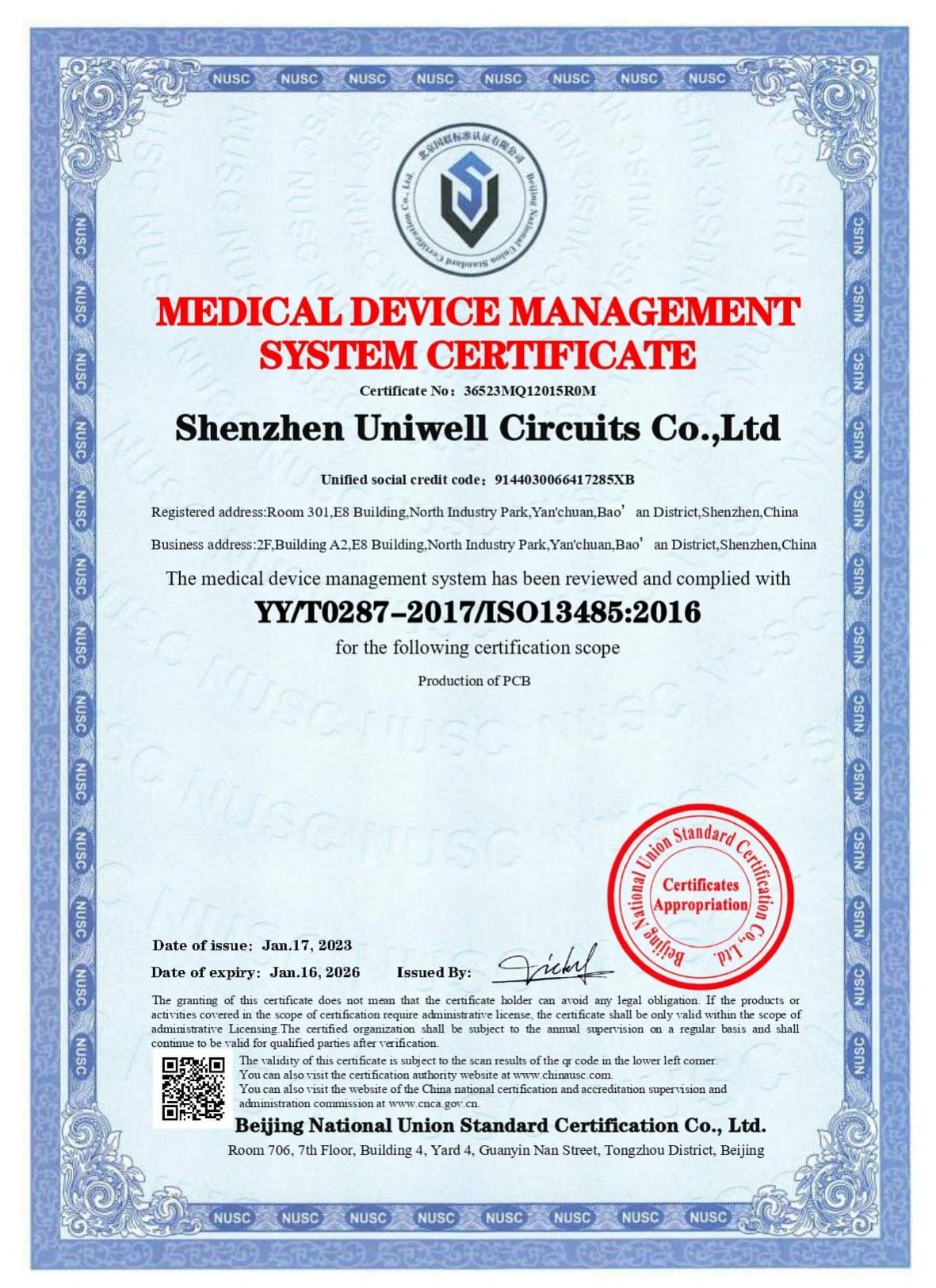
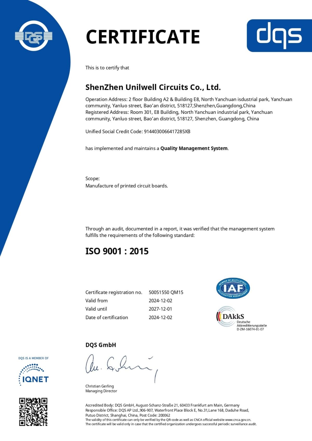
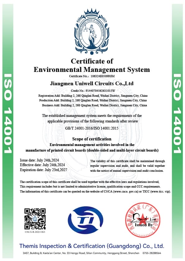
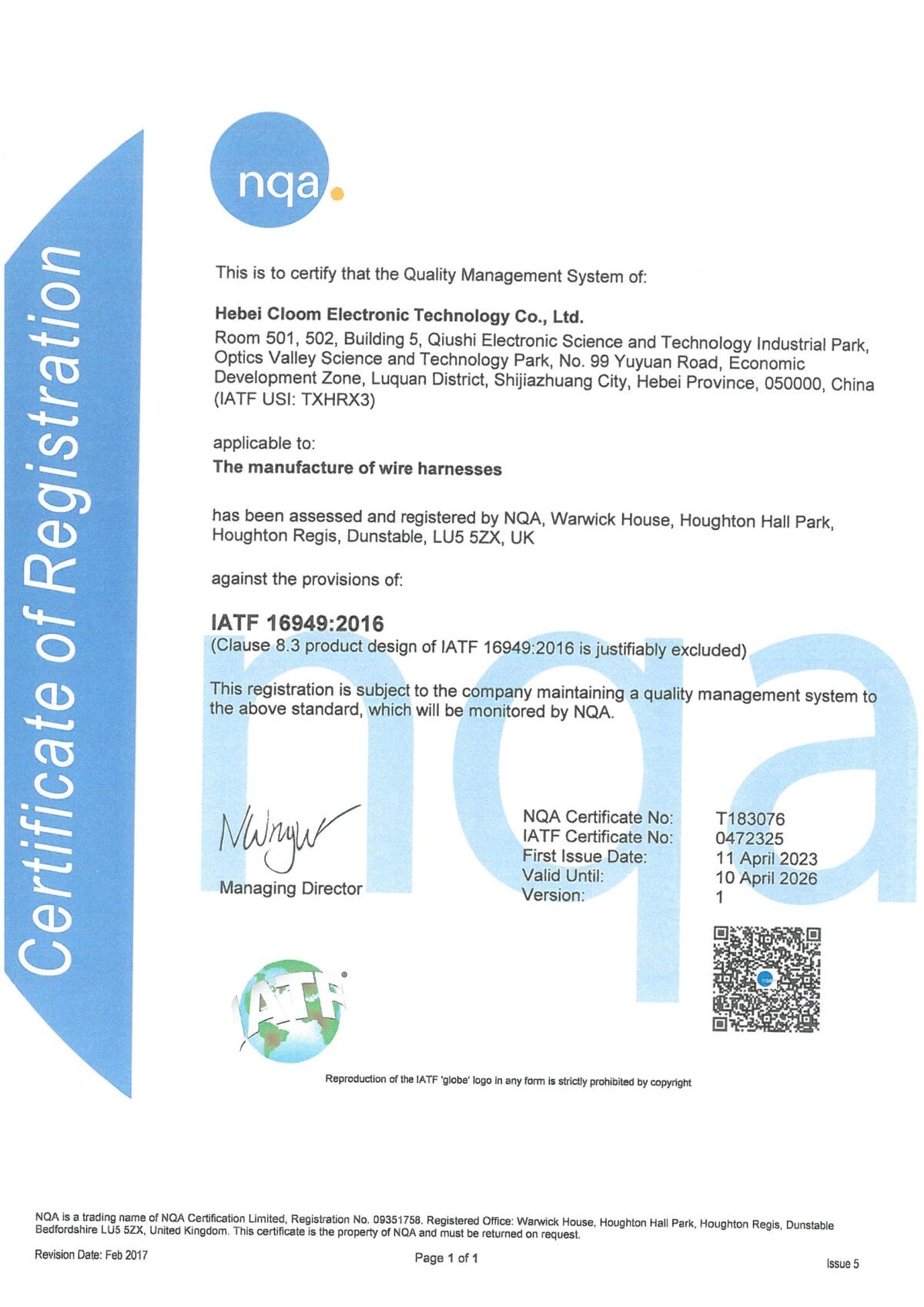
ISO9001 ISO13485
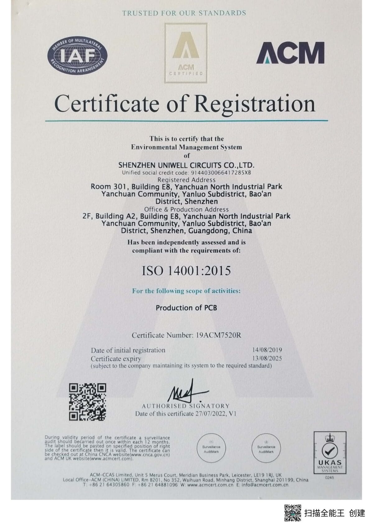
ISO14001

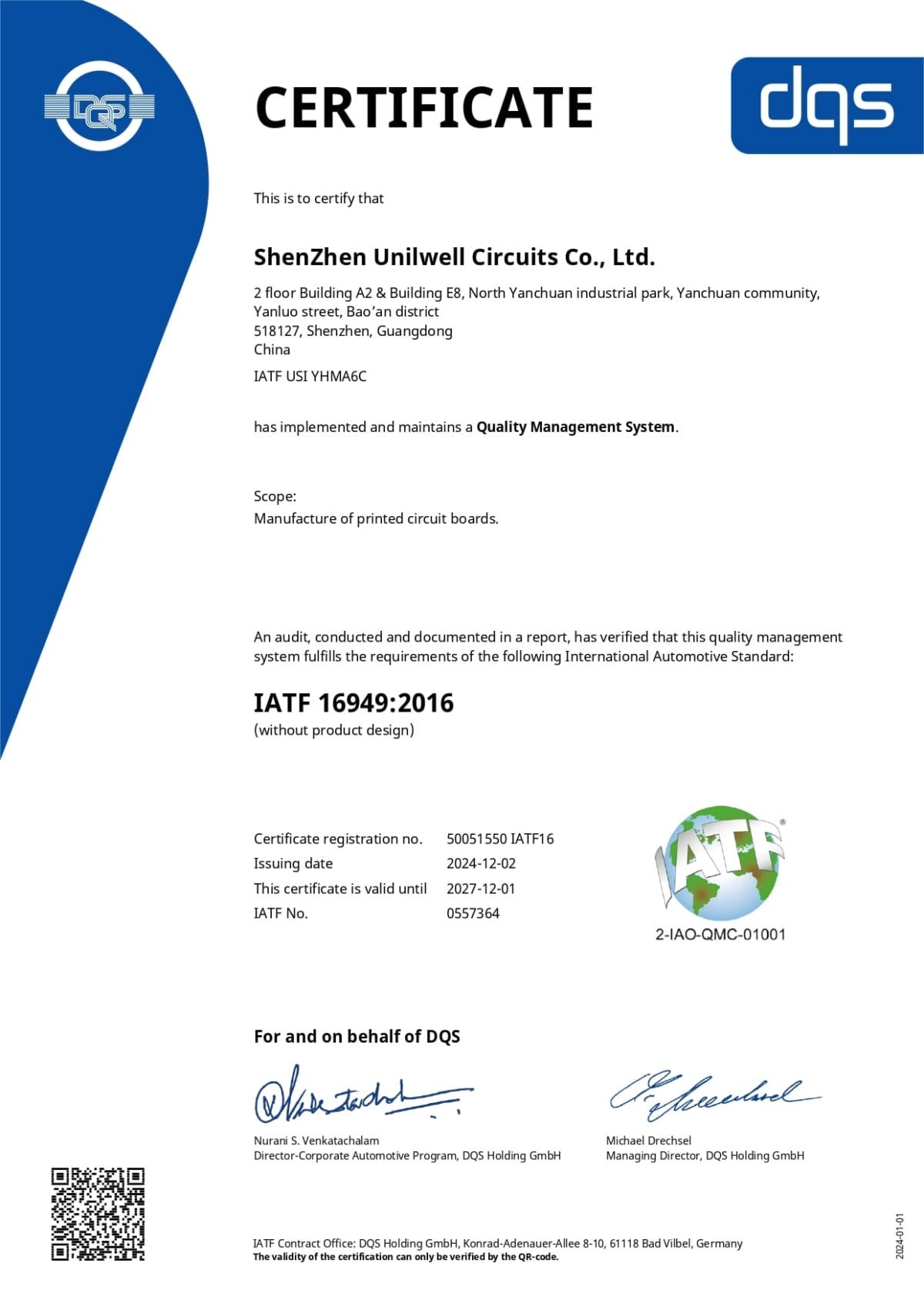
IATF
16949
IPC-A-610H International
Certification

Fully Automated
AOI Inspection

High-Frequency Expertise

Advanced Manufacturing Processes

Quality & Compliance

Turnkey Sourcing

Fast Turnarounds

Excellent Support
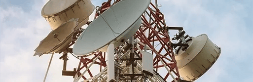
Telecommunications Infrastructure (Cell Towers & Satellites)
You’ll find telecom PCBs in tower modules and satellite communication systems, built to endure outdoor conditions and support high-frequency signal handling.
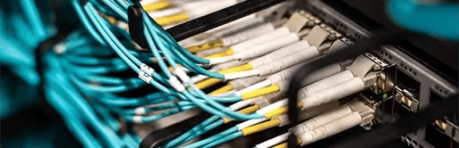
Networking & Office Communications Equipment
PCBs power routers, modems, VoIP devices, and switching systems. They serve as the electronic backbone for office and enterprise-level communications.
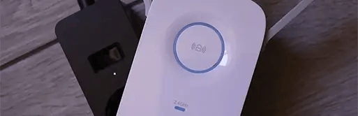
Wireless Access & Antenna Systems
Specialized PCB boards support wireless base stations, signal boosters and custom antenna modules, enabling seamless high speed data transmission.

LED Displays & Indicators in Telecom Gear
Printed circuit boards form the basis of control and interface panels, including status indicators and LED displays used in telecommunications devices.

High Frequency

Tighter Tolerances

Specialized Materials

RF Testing

Submit Your PCB Design
Upload your Gerber files or use our easy online PCB design tool to create your board layout. Make sure your files are complete and correctly formatted to ensure smooth processing and production accuracy.

Select Your PCB Specifications
Customize your order by choosing the technical specifications—number of layers, board dimensions, thickness, copper weight, solder mask color, surface finish, and more. Our intuitive interface helps you configure everything based on your project’s needs.

Get an Instant Quote
Once your design and specs are in place, you'll receive a transparent, instant quote. Pricing updates in real time as you modify options, so you can adjust your selections to match your budget before placing the order.

Confirm Order & Make Payment
Review your entire order for accuracy, including file previews and selected specs. After confirmation, proceed to secure checkout and choose your preferred payment method. You’ll receive an email confirmation with order details.

Production & Delivery
Your PCB moves into production immediately. We’ll keep you updated throughout the manufacturing process. Once completed, your boards are carefully packed and shipped to your door, with tracking information provided for your convenience.


Hommer Zhao
Founder and Chief Editor – Hommer Zhao
Welcome! I’m Hommer Zhao, the founder and Chief Editor of WellPCB. With years of experience in the PCB industry, I’m committed to making sure our content is both accurate and helpful. We’re proud to serve a growing community of over 4,000 customers worldwide, and our goal is to provide you with the best resources and support. Your satisfaction is our top priority, and we’re here to help you every step of the way!

Jesse Holland
Technical Manager – Jesse Holland
Hi, I’m Jesse Holland, an Engineer and Technical Manager at WellPCB. With years of experience in PCB design and engineering, I’m here to ensure that every project we work on meets the highest technical standards. I lead our team, focusing on precision and innovation, collaborating closely with clients to provide tailored solutions and expert guidance. Whether you’re facing a complex design challenge or need advice on technical aspects, I’m here to ensure your project is a success from start to finish.

Nathan Jensen
Purchasing Manager – Nathan Jensen
Hi, I’m Nathan Jenson, the Purchasing Manager at WellPCB. I’m responsible for sourcing the best materials and components to ensure our products meet the highest quality standards. With my extensive experience in procurement, I work closely with suppliers to secure reliable and cost-effective solutions while maintaining strong relationships to support our operations. I aim to ensure every project runs smoothly by providing the resources needed to deliver on time and to your satisfaction.

Emma
Sales Manager – Emma
Hey, I am Emma, sales manager at WellPCB. I studied electronic science and technology at university and have served customers for PCB and PCB Assembly service for several years.
I enjoy communicating with customers and our technicians to solve problems, and customers always say, "It's great to have you onboard".
It is my pleasure and honour to be helpful. Contact me now, and you'll know.

Bella and Cassiel
Sales Representatives – Bella and Cassiel
We’re Bella and Cassiel, your dedicated sales representatives at WellPCB. With our extensive knowledge of the PCB industry, we’re here to provide exceptional service and support. We take the time to understand your unique needs and are always ready to offer tailored solutions and advice. Whether you need product recommendations, assistance with your orders, or simply have a question, we’re here to ensure your experience is smooth and seamless at every step.

Mandy and Wendy
Sales Representatives – Mandy and Wendy
We’re Mandy and Wendy, your friendly sales representatives at WellPCB. Passionate about helping our customers, we bring a wealth of experience in the PCB industry to provide you with the best solutions and service. We take pride in building strong relationships with our clients, understanding their specific needs, and offering personalised support to ensure their satisfaction. Whether you’re looking for advice, product information, or assistance with any part of your order, we’re here to make your experience as smooth and efficient as possible.
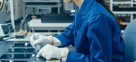
PCB Assembly
PCB assembly plays a vital role in telecommunications infrastructure. For example, as a key component of core network equipment, it facilitates data transmission, switching, and signal processing.
Assembly Process:
Soldering: Small components such as capacitors and resistors are precisely soldered using SMT to ensure reliable electrical connections. Interfaces, heat sinks, and other components are soldered using plug-in soldering to ensure a secure physical connection, ensuring proper signal transmission and heat dissipation.
Cable Connections: Connections such as ribbon cables and power cables must strictly adhere to pinout definitions and insertion and removal force standards. Loose ribbon cables, such as those shown in the image, can disrupt signal transmission and cause display anomalies.
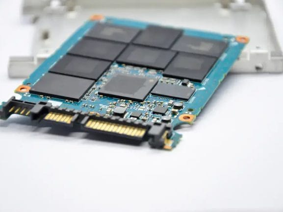
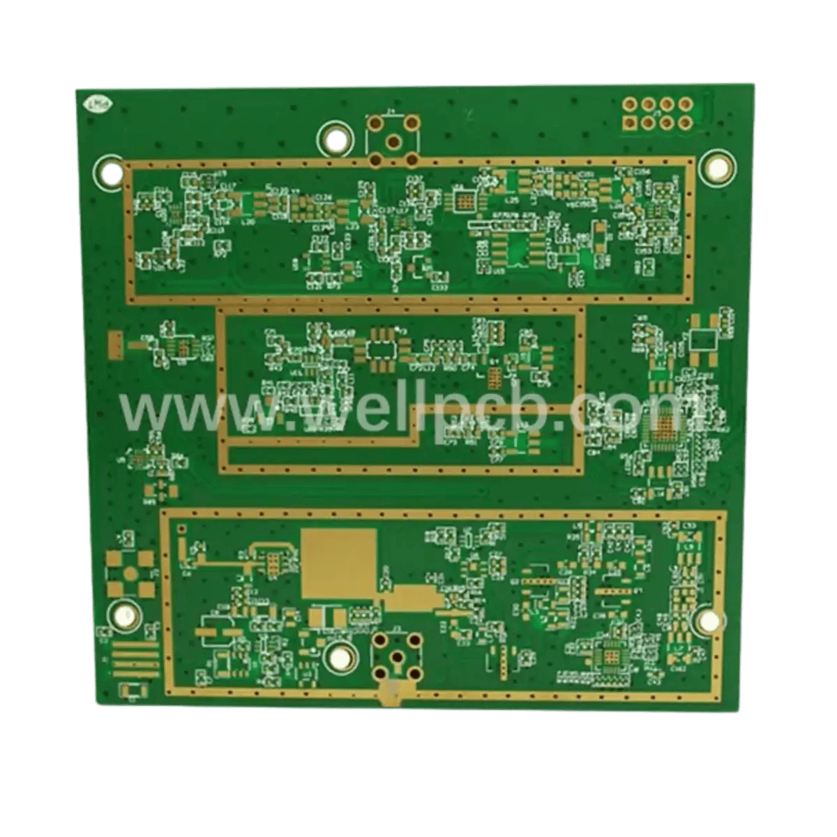
PCB Assembly
The board in the picture is a main control board manufactured according to customer requirements, and has relatively wide applicability in the telecommunications field. For example, server storage and cloud computing services, data transmission of network devices and communication base stations, etc.
Special Process:
- •High-precision SMT processing: Extremely small pin pitch and high assembly accuracy requirements.
- •Multi-layer PCB design and manufacturing: Multiple complex processes and extremely high inter-layer alignment requirements to ensure accurate signal transmission.
- •Packaging technology and reliability testing: To ensure the reliable operation of PCBA in various complex environments, a series of strict reliability tests needs to be carried out after the manufacturing is completed.
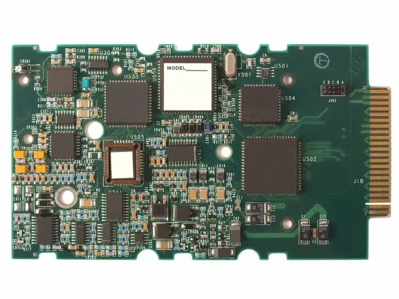
PCB Assembly
This case study focuses on a PCBA used in the telecommunications sector.
The board carries multiple types of chips (such as signal processing chips and memory chips) to support functions such as signal modulation and demodulation, data caching, and forwarding in telecommunications equipment.
Telecommunications networks place stringent demands on signal integrity and interference immunity. This circuit board utilizes a multi-layer PCB design to effectively isolate signals of different frequency bands and reduce electromagnetic interference (EMI). This ensures accurate signal transmission in the complex electromagnetic environment of telecommunications base stations, preventing problems such as call noise and data packet loss caused by signal crosstalk.