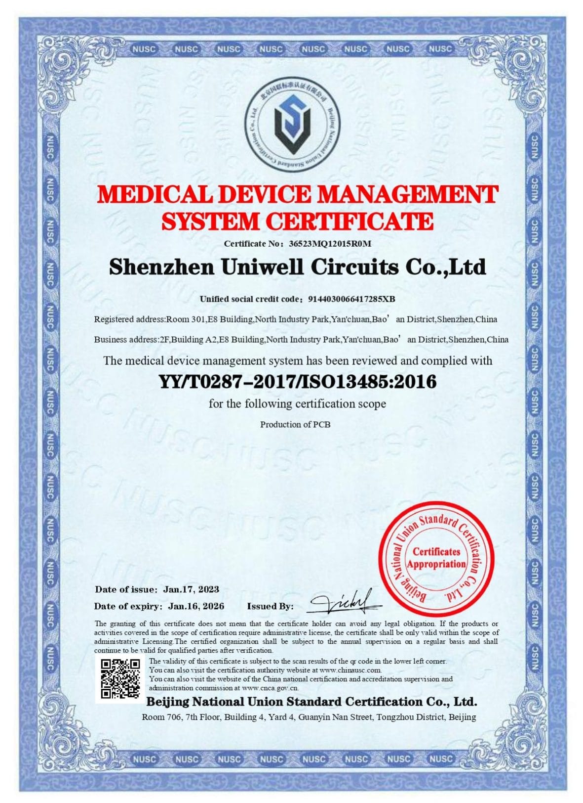
ISO9001 ISO13485
ISO14001

IATF
16949
IPC-A-610H International
Certification

Fully Automated
AOI Inspection

Proven Expertise in Low Loss PCB Fabrication

Comprehensive Manufacturing Services

Rapid Production with Volume Flexibility

Stringent Quality and Reliability Testing

Cost-Optimized Low Loss PCB Solutions

Engineering and Technical Support

Telecommunications and 5G Infrastructure
In 5G base stations, small cells and distributed antenna systems, low loss PCBs handle frequencies above 28 GHz with low insertion loss for stable, long-distance transmission.
Controlled impedance and low dielectric constant materials ensure consistent performance in massive MIMO and beamforming systems.

Automotive Radar and ADAS Systems
Advanced Driver Assistance Systems and radar sensors operating at 24 GHz and 77 GHz rely on low loss PCBs to maintain accuracy in detecing objects and lane assist functions.
High frequency laminates and low coefficient of thermal expansion materials withstand wide temperature swings in automotive environments.

Medical Imaging and Diagnostic Equipment
MRI, CT and ultrasound systems use low loss PCBs to preserve signal clarity in high resolution imaging.
Low-loss materials reduce dielectric loss and EMI susceptibility, while maintaining a stable impedance during continuous operations.

High-Speed Data Centers and Networking Hardware
Switches, routers and optical transceivers in data centers require low loss PCBs to meet signal integrity targets at 25 to 112 Gbps.
These boards maintain low transmission loss for high speed communication and reduce jitter in PAM4 signaling.

Consumer Electronics with High-Speed Interfaces
Smartphones, tablets and wearable devices with 5G, Wi-Fi 6E, and HDMI 2.1 connections benefit from low loss PCBs to ensure stable high frequency performance in compact rigid-flex PCB designs. These boards balance high density interconnects with efficient thermal management for reliable consumer use.
PTFE-Based Laminates
Rogers RO4003C and RO4350B Laminates
Isola 370HR and Isola 408HR Laminates
Panasonic Megtron 6

Material Selection Based on Frequency and Loss Budget

Trace Geometry and Routing Best Practices

Minimizing EMI and Crosstalk

Thermal Management in High-Power Applications

Submit Your PCB Design
Upload your Gerber files or use our easy online PCB design tool to create your board layout. Make sure your files are complete and correctly formatted to ensure smooth processing and production accuracy.

Select Your PCB Specifications
Customize your order by choosing the technical specifications—number of layers, board dimensions, thickness, copper weight, solder mask color, surface finish, and more. Our intuitive interface helps you configure everything based on your project’s needs.

Get an Instant Quote
Once your design and specs are in place, you'll receive a transparent, instant quote. Pricing updates in real time as you modify options, so you can adjust your selections to match your budget before placing the order.

Confirm Order & Make Payment
Review your entire order for accuracy, including file previews and selected specs. After confirmation, proceed to secure checkout and choose your preferred payment method. You’ll receive an email confirmation with order details.

Production & Delivery
Your PCB moves into production immediately. We’ll keep you updated throughout the manufacturing process. Once completed, your boards are carefully packed and shipped to your door, with tracking information provided for your convenience.


Hommer Zhao
Founder and Chief Editor – Hommer Zhao
Welcome! I’m Hommer Zhao, the founder and Chief Editor of WellPCB. With years of experience in the PCB industry, I’m committed to making sure our content is both accurate and helpful. We’re proud to serve a growing community of over 4,000 customers worldwide, and our goal is to provide you with the best resources and support. Your satisfaction is our top priority, and we’re here to help you every step of the way!

Jesse Holland
Technical Manager – Jesse Holland
Hi, I’m Jesse Holland, an Engineer and Technical Manager at WellPCB. With years of experience in PCB design and engineering, I’m here to ensure that every project we work on meets the highest technical standards. I lead our team, focusing on precision and innovation, collaborating closely with clients to provide tailored solutions and expert guidance. Whether you’re facing a complex design challenge or need advice on technical aspects, I’m here to ensure your project is a success from start to finish.

Nathan Jensen
Purchasing Manager – Nathan Jensen
Hi, I’m Nathan Jenson, the Purchasing Manager at WellPCB. I’m responsible for sourcing the best materials and components to ensure our products meet the highest quality standards. With my extensive experience in procurement, I work closely with suppliers to secure reliable and cost-effective solutions while maintaining strong relationships to support our operations. I aim to ensure every project runs smoothly by providing the resources needed to deliver on time and to your satisfaction.

Emma
Sales Manager – Emma
Hey, I am Emma, sales manager at WellPCB. I studied electronic science and technology at university and have served customers for PCB and PCB Assembly service for several years.
I enjoy communicating with customers and our technicians to solve problems, and customers always say, "It's great to have you onboard".
It is my pleasure and honour to be helpful. Contact me now, and you'll know.

Bella and Cassiel
Sales Representatives – Bella and Cassiel
We’re Bella and Cassiel, your dedicated sales representatives at WellPCB. With our extensive knowledge of the PCB industry, we’re here to provide exceptional service and support. We take the time to understand your unique needs and are always ready to offer tailored solutions and advice. Whether you need product recommendations, assistance with your orders, or simply have a question, we’re here to ensure your experience is smooth and seamless at every step.

Mandy and Wendy
Sales Representatives – Mandy and Wendy
We’re Mandy and Wendy, your friendly sales representatives at WellPCB. Passionate about helping our customers, we bring a wealth of experience in the PCB industry to provide you with the best solutions and service. We take pride in building strong relationships with our clients, understanding their specific needs, and offering personalised support to ensure their satisfaction. Whether you’re looking for advice, product information, or assistance with any part of your order, we’re here to make your experience as smooth and efficient as possible.
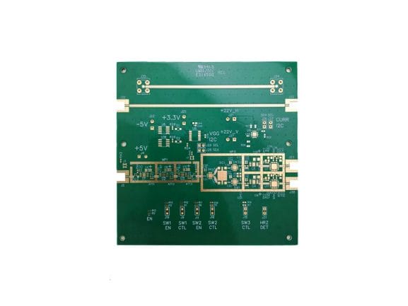
PCB Assembly
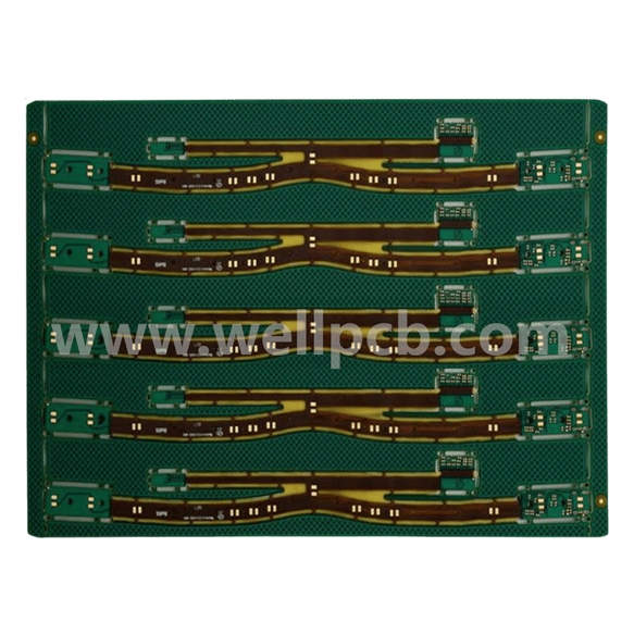
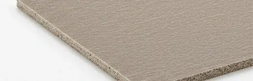
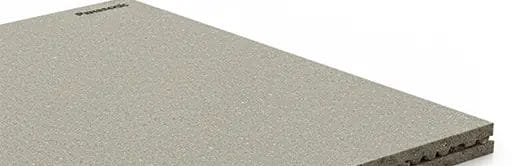
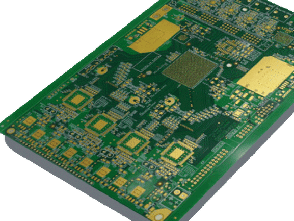
This case study demonstrates a low loss PCB fabricated using the RO4350B. This material has a wide range of applications and requires a specific manufacturing process.
Applications:
Wireless communications: Its low loss characteristics reduce signal attenuation during transmission, improving signal quality and base station coverage. Test and measurement equipment: The RO4350B low-loss PCB meets the performance requirements of high-frequency equipment.
Satellite communications: The RO4350B low-loss PCB minimizes excess transmission loss, ensuring the strength and quality of received signals.
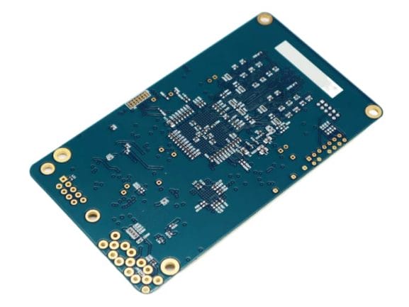
PCB Assembly
High-layer low-loss PCBs provide stable signal transmission, meeting the stringent signal transmission requirements of these devices. They are suitable for communications, navigation, and control systems in aerospace equipment.
Manufacturing Process:
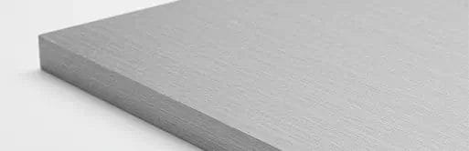
- •Low-loss substrate materials: Select materials with low dielectric constant (Dk) and low dissipation factor (Df).
- •Impedance Control: Control impedance deviation and optimize circuit design.
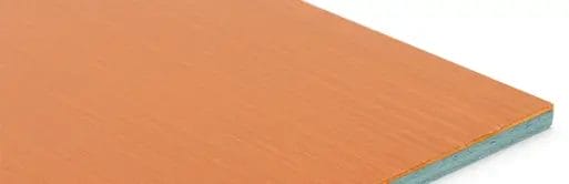
- •Surface Treatment: Requires strong oxidation resistance to improve soldering yield; typically uses processes such as immersion gold and immersion silver.
PCB Assembly
This low-loss PCB is used in medical diagnostic equipment, such as magnetic resonance imaging (MRI) and computed tomography (CT), which require extremely high signal accuracy and stability.
Low-loss PCBs can reduce signal interference and loss, ensuring accurate images and data are captured, providing a reliable basis for disease diagnosis.