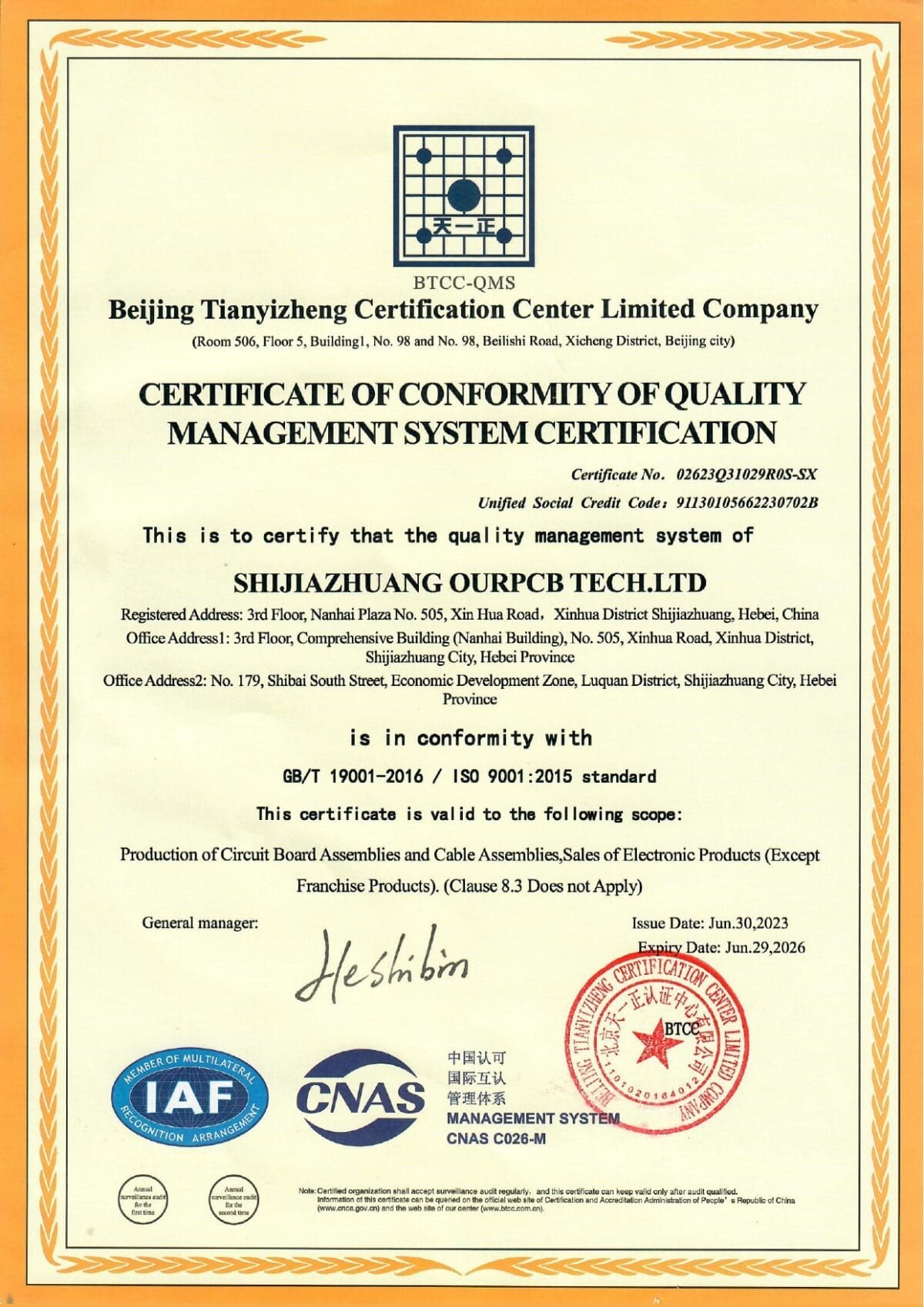
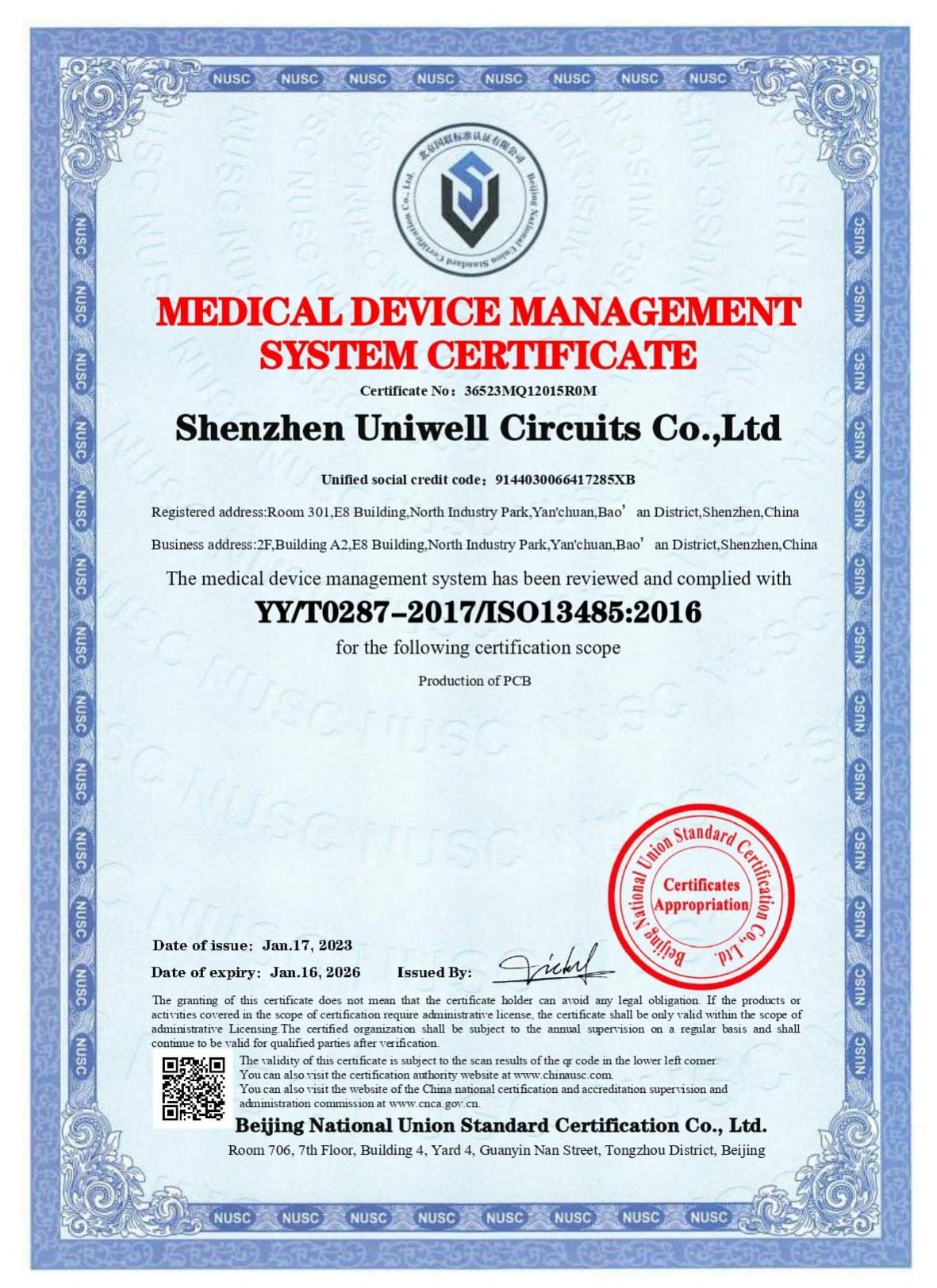
ISO9001 ISO13485
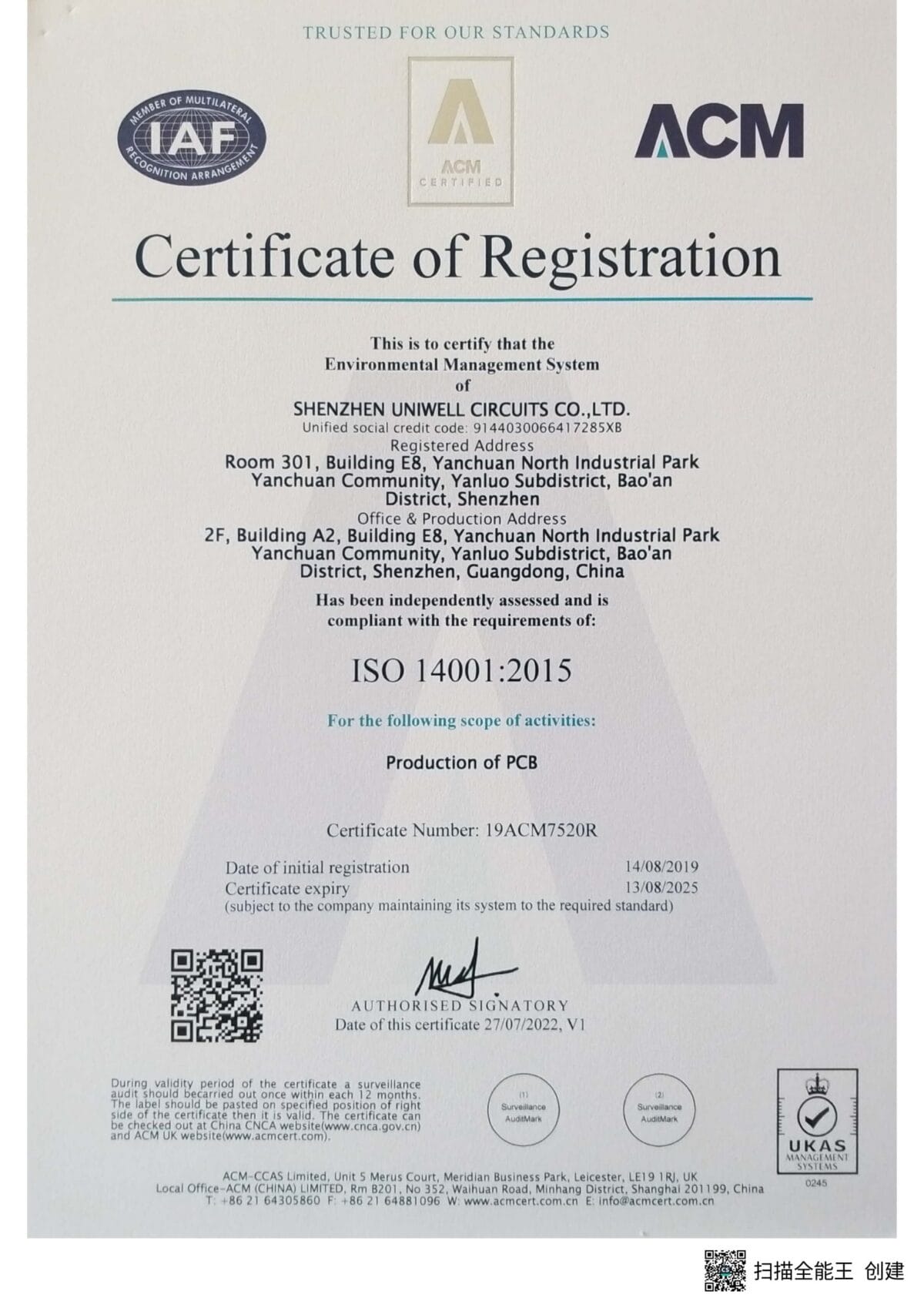
ISO14001

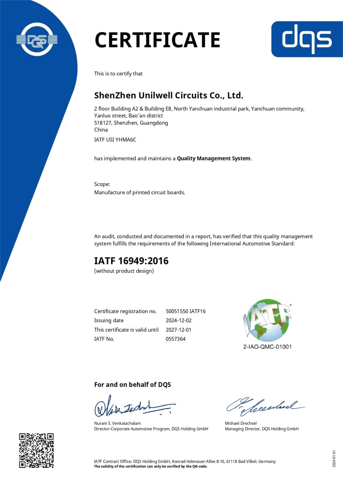
IATF
16949
IPC-A-610H International
Certification

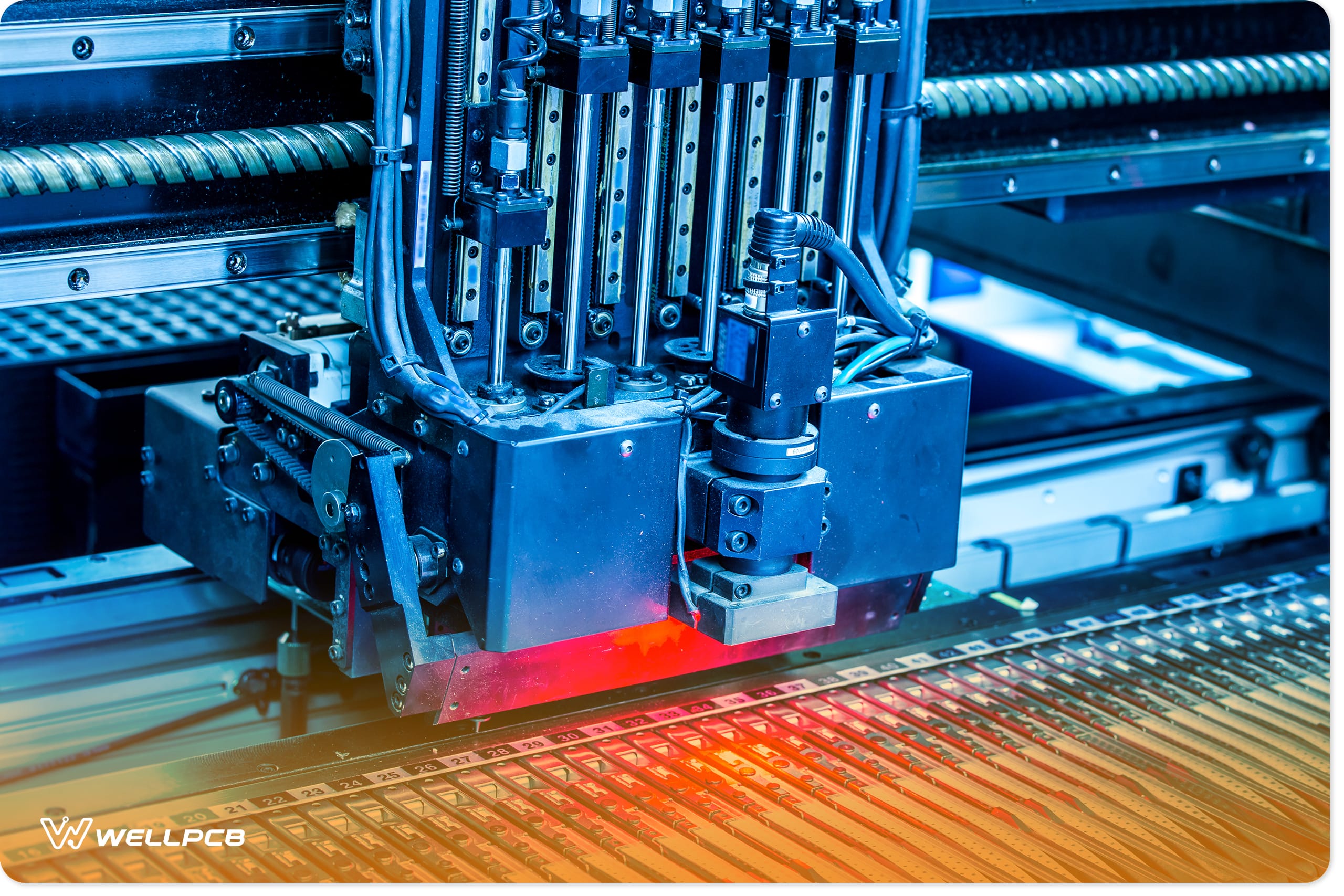
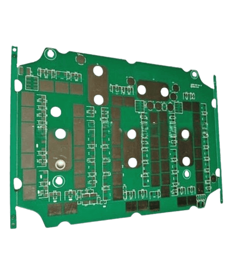
Fully Automated
AOI Inspection

18+ Years of Focused MCPCB Experience

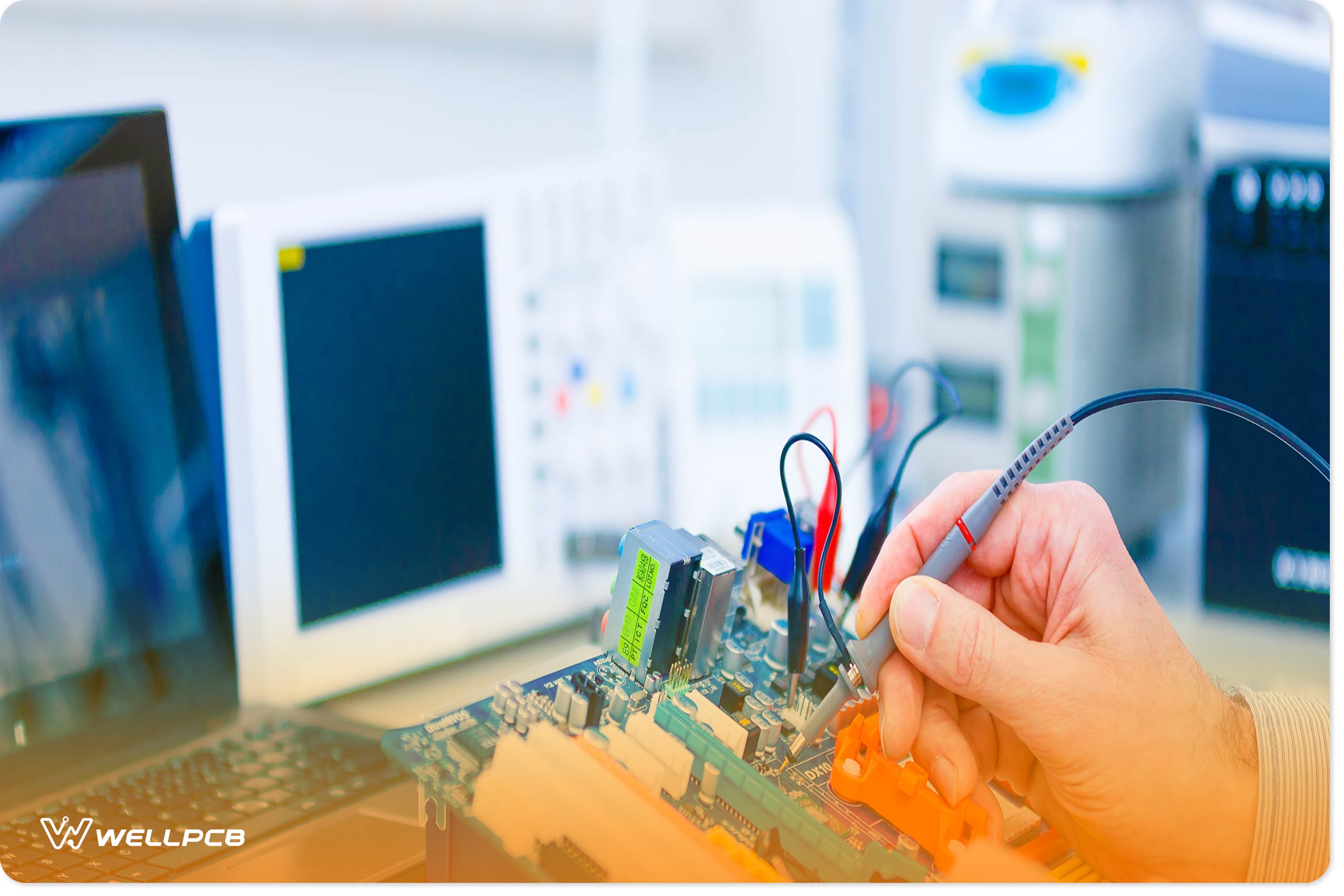
Precision Testing and Inspection

Extensive Material Compatibility

Proactive Technical Support

Manufacturing Cost Efficiency

Scalable Production Capacity

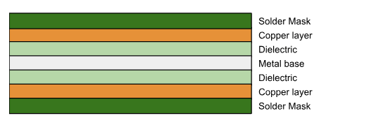
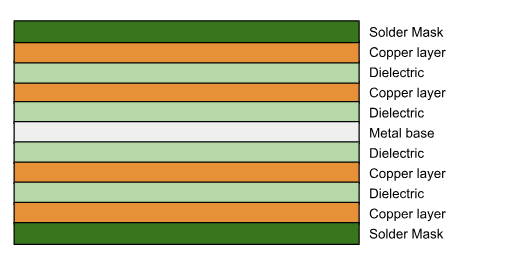
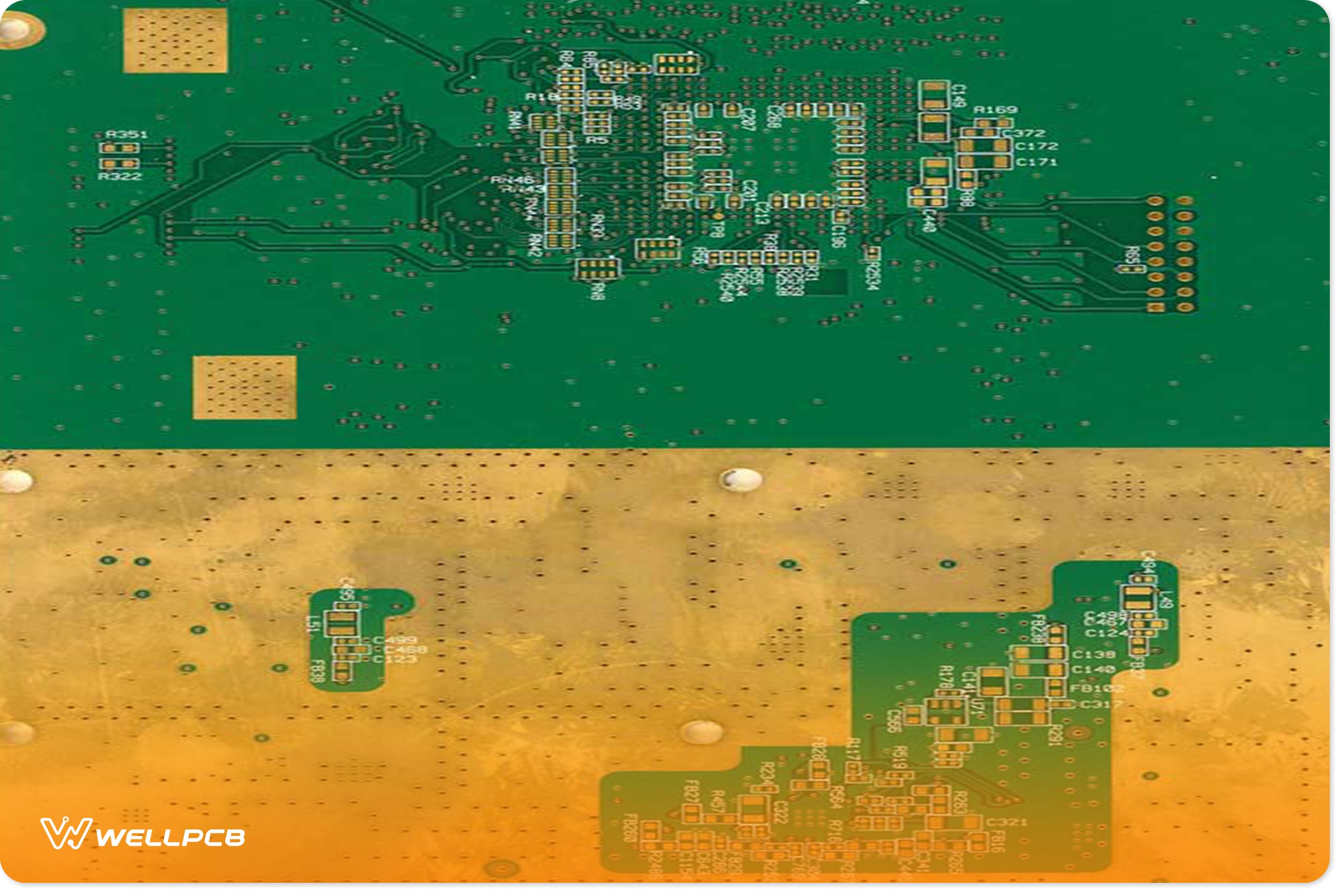
Aluminum Core PCBs

Copper Core PCBs

Steel or Brass Core PCBs

Metal Core Thicknesses

Design & Output
We begin by importing customer design data into CAM software to generate fabrication tooling, including Gerber layers, drill files, and impedance models.
Our DFM review checks dielectric thickness (±10 μm tolerance), pad/via clearance to the metal core (≥0.3 mm required), and verifies stack-up compatibility for heat-spreading efficiency and controlled Z-axis expansion.
Film Printing
Phototools are laser-plotted at 25,000–50,000 DPI to achieve sub-50 μm trace precision. Dry film photoresist is laminated under 0.5 to 1.2 MPa pressure at ~110 °C.
Tension control and thermal stability during lamination are key to avoid shifting on thick-core substrates, especially those with core thicknesses above 2.4 mm.
Image Transfer
Laminated panels are exposed to UV light at 365 to 405 nm to harden the photoresist on copper areas. Unexposed areas are removed during development.
Track width control is maintained within ±10%, with target copper surface roughness (Ra) between 1.0 and 1.5 μm to ensure reliable downstream bonding.
Etching
Etching is performed with acid-based or ammoniacal chemistries, depending on copper weight and line density.
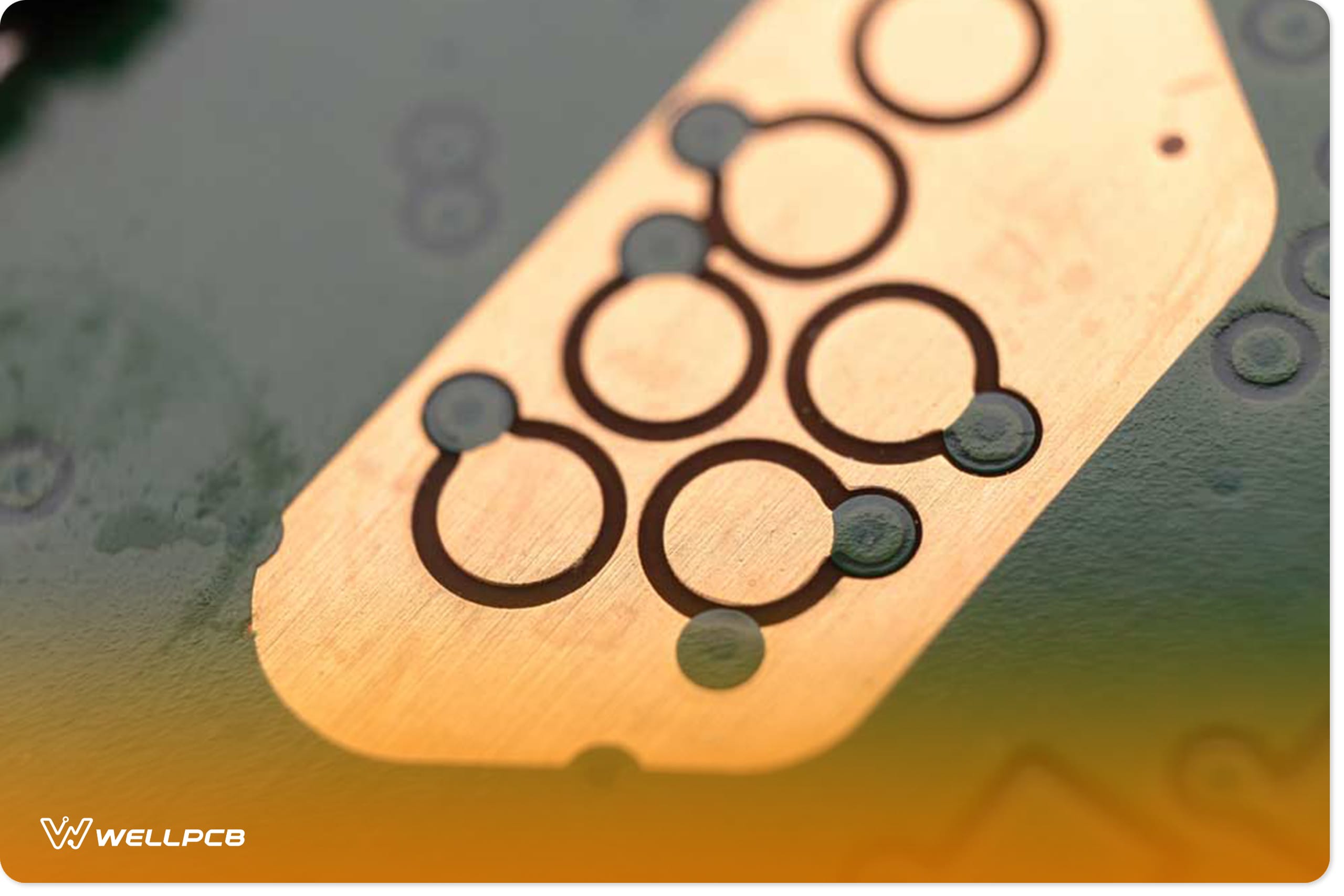
Trace geometries down to 0.15 mm with 0.15 mm spacing are supported, with etch uniformity balanced through solution flow rate, dwell time, and copper surface area.
Drilling & Plating
Minimum hole diameters of 0.2 mm are supported, with copper plating thickness maintained at 25 to 30 μm using pulse current deposition.

Solder Mask Application
Solder mask is applied by screen printing or spray coating, then UV and thermal cured. Thickness is maintained at 20 to 35 μm.
On single-sided MCPCBs, the solder mask is applied only to the component side to ensure clean dielectric exposure and avoid reflow issues.
Surface Finishing
Surface treatments include ENIG (120 to 150 μin Ni / 2–5 μin Au), OSP (0.2 to 0.5 μm), and HASL.
Finish selection is based on the assembly process and pad metallization compatibility. Each finish is tested for thickness uniformity and wetting behavior.
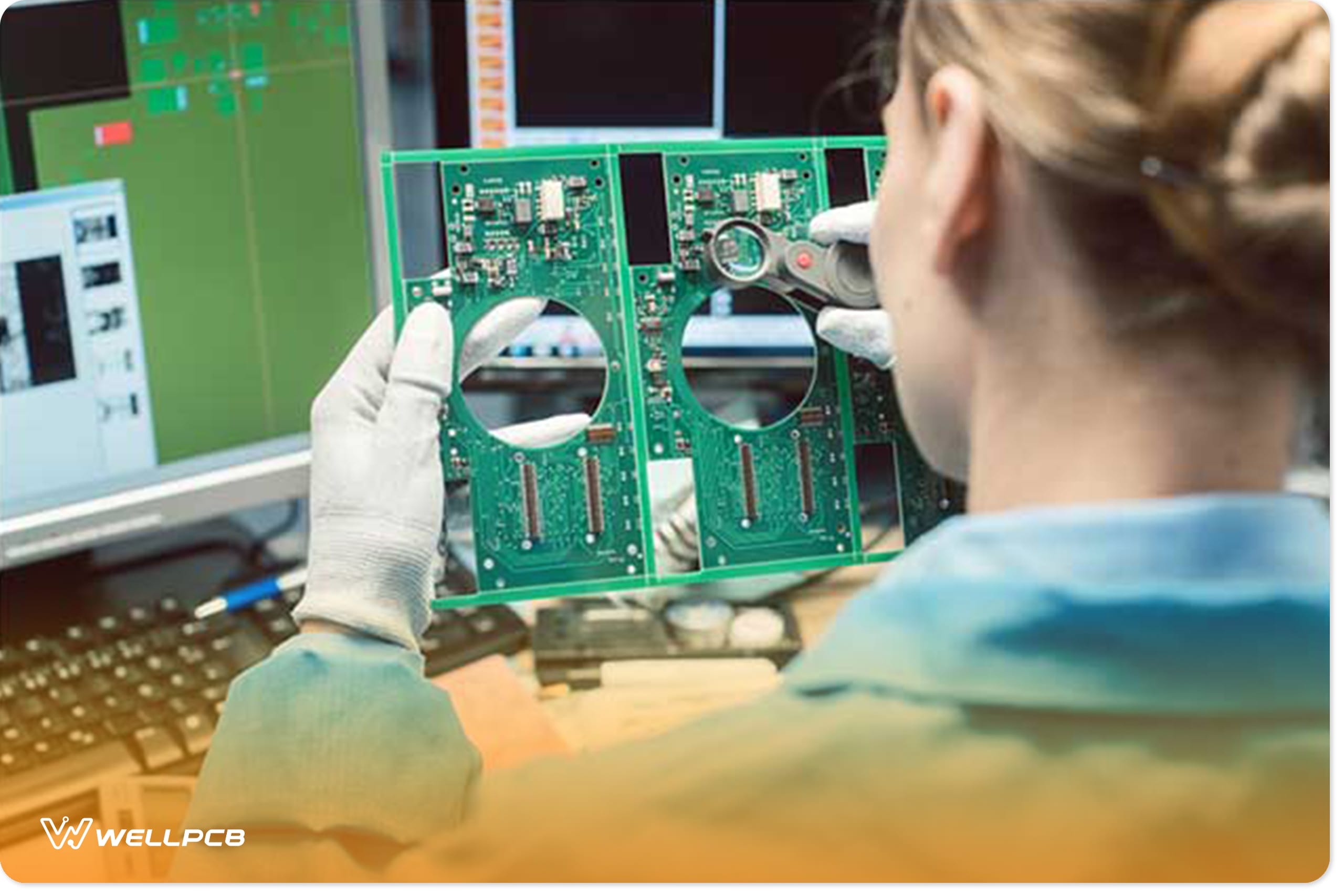
Inspection & Testing
Final inspection includes AOI, flying probe or fixture-based electrical testing, and X-ray verification of filled or insulated vias.
Impedance testing is performed where controlled line widths are specified. Dimensional conformity and flatness are verified to IPC-6012 guidelines.

Submit Your PCB Design
Upload your Gerber files or use our easy online PCB design tool to create your board layout. Make sure your files are complete and correctly formatted to ensure smooth processing and production accuracy.

Select Your PCB Specifications
Customize your order by choosing the technical specifications—number of layers, board dimensions, thickness, copper weight, solder mask color, surface finish, and more. Our intuitive interface helps you configure everything based on your project’s needs.

Get an Instant Quote
Once your design and specs are in place, you'll receive a transparent, instant quote. Pricing updates in real time as you modify options, so you can adjust your selections to match your budget before placing the order.

Confirm Order & Make Payment
Review your entire order for accuracy, including file previews and selected specs. After confirmation, proceed to secure checkout and choose your preferred payment method. You’ll receive an email confirmation with order details.

Production & Delivery
Your PCB moves into production immediately. We’ll keep you updated throughout the manufacturing process. Once completed, your boards are carefully packed and shipped to your door, with tracking information provided for your convenience.


Hommer Zhao
Founder and Chief Editor – Hommer Zhao
Welcome! I’m Hommer Zhao, the founder and Chief Editor of WellPCB. With years of experience in the PCB industry, I’m committed to making sure our content is both accurate and helpful. We’re proud to serve a growing community of over 4,000 customers worldwide, and our goal is to provide you with the best resources and support. Your satisfaction is our top priority, and we’re here to help you every step of the way!

Jesse Holland
Technical Manager – Jesse Holland
Hi, I’m Jesse Holland, an Engineer and Technical Manager at WellPCB. With years of experience in PCB design and engineering, I’m here to ensure that every project we work on meets the highest technical standards. I lead our team, focusing on precision and innovation, collaborating closely with clients to provide tailored solutions and expert guidance. Whether you’re facing a complex design challenge or need advice on technical aspects, I’m here to ensure your project is a success from start to finish.

Nathan Jensen
Purchasing Manager – Nathan Jensen
Hi, I’m Nathan Jenson, the Purchasing Manager at WellPCB. I’m responsible for sourcing the best materials and components to ensure our products meet the highest quality standards. With my extensive experience in procurement, I work closely with suppliers to secure reliable and cost-effective solutions while maintaining strong relationships to support our operations. I aim to ensure every project runs smoothly by providing the resources needed to deliver on time and to your satisfaction.

Emma
Sales Manager – Emma
Hey, I am Emma, sales manager at WellPCB. I studied electronic science and technology at university and have served customers for PCB and PCB Assembly service for several years.
I enjoy communicating with customers and our technicians to solve problems, and customers always say, "It's great to have you onboard".
It is my pleasure and honour to be helpful. Contact me now, and you'll know.

Bella and Cassiel
Sales Representatives – Bella and Cassiel
We’re Bella and Cassiel, your dedicated sales representatives at WellPCB. With our extensive knowledge of the PCB industry, we’re here to provide exceptional service and support. We take the time to understand your unique needs and are always ready to offer tailored solutions and advice. Whether you need product recommendations, assistance with your orders, or simply have a question, we’re here to ensure your experience is smooth and seamless at every step.

Mandy and Wendy
Sales Representatives – Mandy and Wendy
We’re Mandy and Wendy, your friendly sales representatives at WellPCB. Passionate about helping our customers, we bring a wealth of experience in the PCB industry to provide you with the best solutions and service. We take pride in building strong relationships with our clients, understanding their specific needs, and offering personalised support to ensure their satisfaction. Whether you’re looking for advice, product information, or assistance with any part of your order, we’re here to make your experience as smooth and efficient as possible.
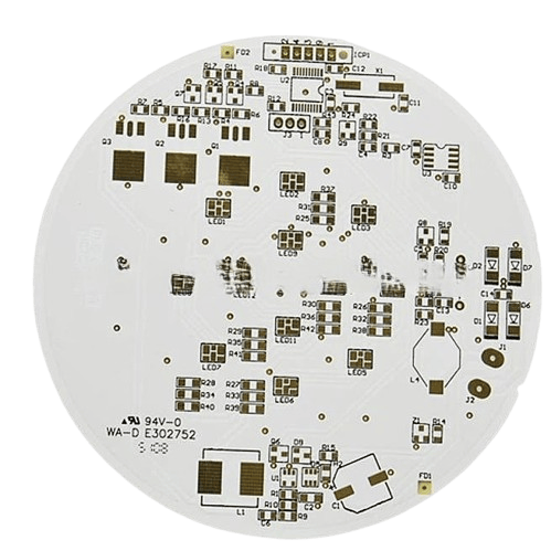
Case Study
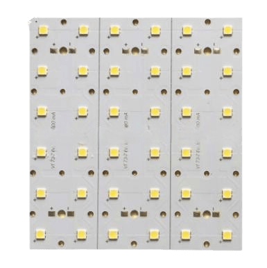
This single-layer aluminum PCB is built to support high thermal conductivity, mechanical stability, and efficient power handling, ideal for LED lighting systems, power modules, and industrial drivers. With a 1.0mm aluminum core and 70μm copper, it ensures superior heat dissipation and durability.
Product Specifications:
- PCB Type: 3W Aluminum PCB (Metal Core PCB)
- Layer Count: 1 (Single-sided)
- Total Thickness: 1.05 mm
- Core Material: Aluminum base, 1.0 mm
- Copper Thickness: 70 μm (2 oz)
- Surface Finish: Lead-Free HASL (LF HASL)
- Minimum Line Width/Spacing: 20 mil (0.508 mm)
- Thermal Conductivity: Typically 2–3 W/m·K (material-dependent)
- Application: Power modules, LED lighting, automotive
Case Study
This single-layer copper-based PCB is engineered for LED lighting applications that demand excellent thermal performance, electrical insulation, and durability. With 2 oz copper, OSP surface finish, and high dielectric strength, it delivers both power efficiency and reliable thermal management in compact lighting systems.
Product Specifications:
- Base Material: Copper base with FR-4 / Aluminum / Ceramic / CEM-3 dielectric options
- Layer Count: 1 Layer (Single-sided)
- Copper Thickness: 2 oz (70 μm)
- Finished Board Thickness: 1.6 mm
- Solder Mask Color: White LPI (Liquid Photo Imageable)
- Legend/Silkscreen: Black
- Surface Finis: OSP (Organic Solderability Preservative)
- Thermal Conductivity: 2 W/m·K
- Breakdown Voltage (Dielectric Layer): ≥ 4KV
- Profile / Cutting: CNC Routing + V-Cut
- Application Area: LED Lighting (bulbs, strips, automotive, high-bay lights)
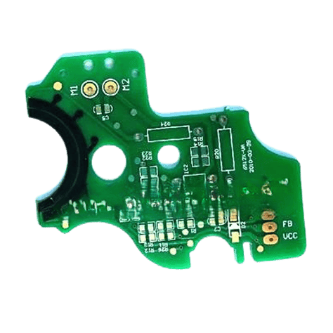
Case Study
This single-layer aluminum base PCB is designed to deliver reliable thermal management, high-density routing, and cost-effective performance. With 1000+ test points, fine-pitch resolution, and a robust 1.6 mm aluminum base, it's ideal for applications such as LED modules, power drivers, and industrial electronics where heat dissipation and signal reliability are critical.
Product Specifications:
- Layer Count: 1 (Single-sided)
- Base Material: Aluminum
- Board Thickness: 1.6 mm
- Copper Thickness: 35 μm (1 oz)
- Minimum Hole Diameter: 0.2 mm
- Minimum Line Width / Spacing: 4 mil / 4 mil (0.1 mm / 0.1 mm)
- Solder Mask Color: Green
- Silkscreen Color: Black
- Surface Finish: HASL (Hot Air Solder Leveling)
- Testing Points: 1000+