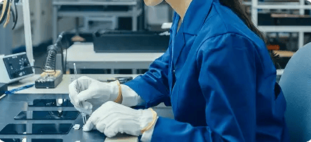
Microvia PCB Supplier
for High-Density HDI Applications
WellPCB is a full service microvia PCB supplier trusted by OEMs in aerospace, medical, automotive and industrial sectors for compact, high-reliability HDI PCBs.
We provide complete PCB manufacturing, assembly and HDI microvia fabrication using 3 to 6 mil laser drilled microvias, stacked microvias, buried vias, and IPC-A-610 grade standards.
With two dedicated fabrication factories, we support prototyping, scalable volume and traceability across all inner layers, vias and interconnects.
- 3 to 6 mil laser drilled microvias with ±15 µm drill accuracy.
- Copper filled stacked microvias, vacuum planarized for pad flatness.
- Blind and buried vias with ≤0.15 mm holes, aspect ratio ≤0.75:1

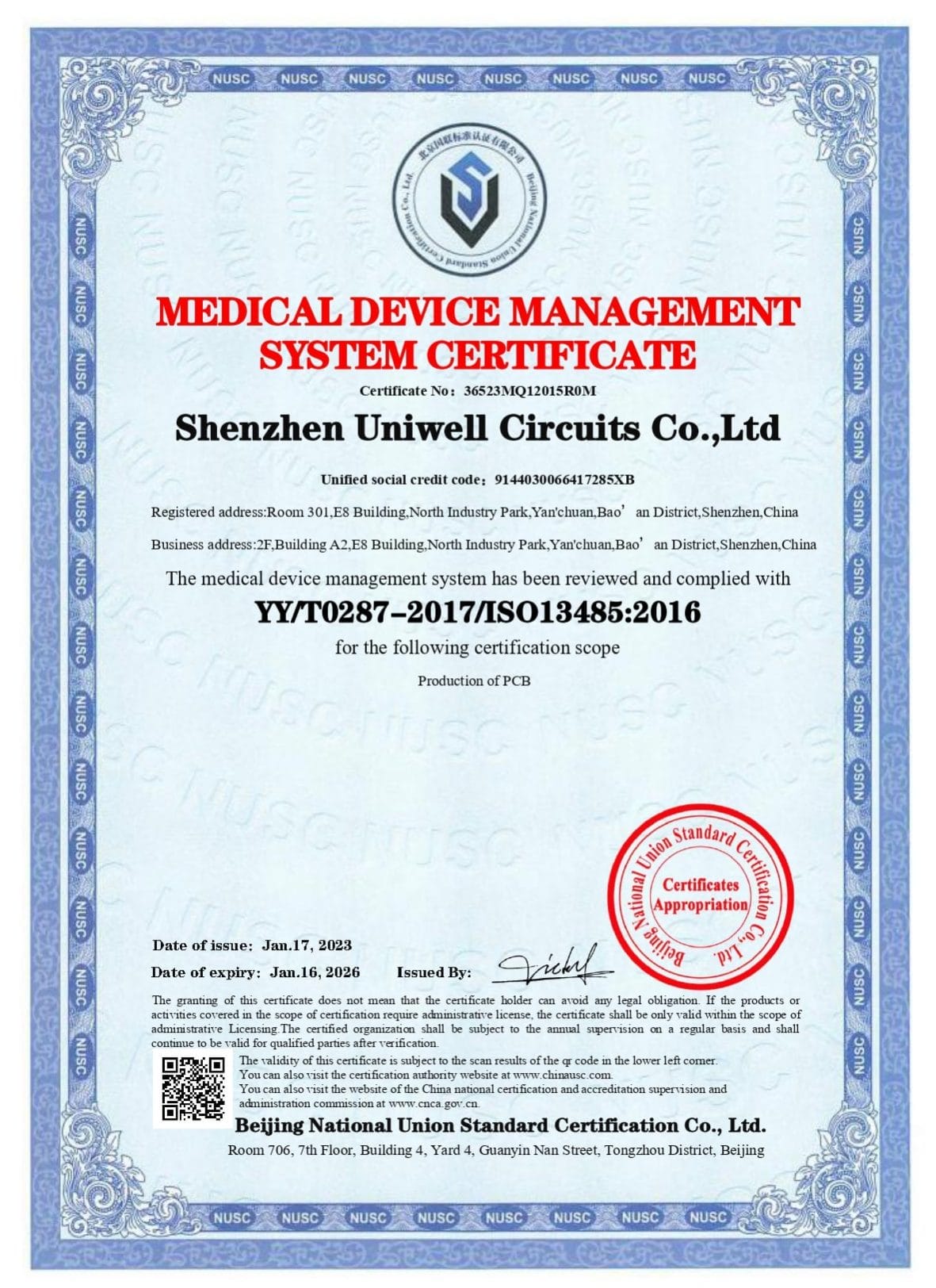
ISO9001 ISO13485
ISO14001

IATF
16949

IPC-A-610H International
Certification

Fully Automated
AOI Inspection
- PCB Manufacturer
- Microvia
Microvia PCB Fabrication for Blind and Buried Vias
WellPCB supports high density applications that depend on compact layer sequencing, precise microvia drilling, and high reliability blind and buried vias across complex HDI PCB architectures.
As a production grade microvia PCB supplier, we fabricate HDI PCBs using sequential lamination and 3 to 6 mil laser-drilled microvias. Blind vias link outer layers to inner ones, while buried vias form connections between internal layers only.
Every via hole is copper plated to 20 to 25 µm, maintaining mechanical and thermal reliability across all HDI stackups.
We process net-defined microvias from validated Gerber, ODB++, or IPC-2581 inputs. Drill spans, layer usage and test point locations are matched to PCB design rules.
Aspect ratio, impedance boundaries, and anti pad geometry are optimized to prevent shorts and support electrical performance.
All buried and blind vias undergo X-ray inspection, microsection sampling and thermal stress testing.
Each HDI PCB is verified to IPC standards before release to PCB assembly, with full traceability maintained throughout lamination, imaging and plating stages.
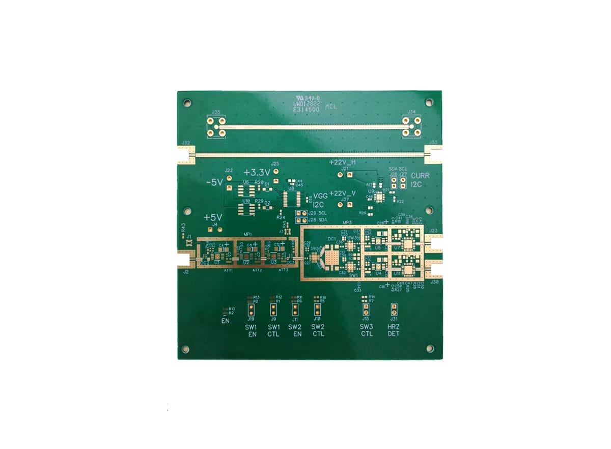
Our Microvia PCB Capabilities
Our laser drilled microvia PCBs are fabricated using stacked, staggered, blind and buried via structures with controlled plating, planarization and impedance performance.
We support HDI stack ups up to 40 layers with IPC-A-610Type I, II, and III builds, copper-filled via-in-pad support, and full process traceability across lamination, inspection, and final PCB assembly.
We use high pulse UV and CO₂ laser systems for via formation, achieving hole diameters between 100 and 150 µm.
Beam control features ±2% energy stability, spot size shaping down to 10 µm, and a programmable drill depth stop based on material thickness.
Via positional accuracy is maintained within ±50 µm through fiducial alignment and real-time beam tracking. These systems allow clean microvia formation across PTFE, FR4, and high Tg cores
Our PCB assemblies are built according to IPC-A-610 Classes 1 through 3 requirements, ensuring solder-joint integrity, component alignment, cleanliness, and overall workmanship meet the stringent criteria for consumer, commercial, and high-reliability applications.
Builds can scale to 36 layers, using low-flow prepreg, vacuum lamination, and step drilling for hybrid via structures.
Stacked microvias are drilled and copper-filled sequentially with each lamination stage, using resin coated foil (RCF) and vacuum copper plating to maintain via verticality.
Staggered vias offset by 0.2 to 0.3 mm reduce cumulative expansion and increase reliability. We maintain aspect ratios of ≤0.75:1 for stacked vias and control interconnect skew with layer-to-layer alignment of ±50 µm across the full HDI stack.
Microvias are filled using electrolytic copper plating at current densities of 20 to 30 ASF, forming via wall thicknesses between 20 and 25 µm.
After plating, vias are planarized using chemical-mechanical polishing (CMP) to maintain pad coplanarity within ±15 µm, supporting stable solder joint formation under BGA packages.
The via fill factor is controlled to ≥95%, eliminating internal voids, improving thermal transfer and preventing solder collapse during reflow.
For via-in-pad builds, filled vias are capped and planarized to a surface tolerance of ±10 μm before the application of the solder mask.
These structures are used with fine-pitch BGA and CSP devices, down to 0.4 mm pitch, with no solder wicking or collapse.
VIPPO structures are verified by X-ray, microsectioning, and SMT trial builds to ensure flatness and joint stability during the PCB assembly process.
Our microvia PCBs are fabricated on FR4, PTFE, LCP, Isola 370HR, Rogers 4003C, and halogen free systems.
Each laminate is selected based on laser ablation profile, glass transition temperature (Tg), Df/Dk targets, and stack up thickness compatibility.
For stacked builds, resin content is adjusted to prevent flow-out and maintain dielectric spacing across inner layers and blind spans.
Each panel undergoes AOI via ring check, pad alignment and annular ring clearance validation.
X-ray inspection ensures internal via fill and concentricity, with inspection resolutions down to 10 µm voxel size.
Microsection analysis confirms plating thickness, resin voids, and via wall adhesion. All buried and blind vias are tested in accordance with IPC acceptance limits.
HDI stack ups are modeled with field solver simulations and manufactured with ±5 Ω tolerance on 50 Ω single-ended and 90 Ω differential traces.
Each microvia layer’s dielectric constant and copper thickness are carefully controlled.
We verify impedance by TDR sampling across stacked via paths on impedance coupons placed on every panel.
Why Choose WellPCB as Your Microvia PCB Supplier?
WellPCB delivers microvia PCB solutions that support fine-pitch routing, tight stack up control, and copper filled interconnections across blind, buried, and stacked via builds.
We manufacture to IPC standards, integrate laser-defined microvia control, and maintain production traceability from prototype to high volume PCB assembly.

Advanced Equipment
Our Shijiazhuang site operates five Siemens SMT lines across 10,000 m², with over 300 technicians, while our Shenzhen assembly facility operates eight Yamaha SMT lines.

Fast Turnaround
Each order uses prequalified stackups, panel tooling, and lamination sequences to ensure consistency from the first article through volume scaling.

Quality Assurance
We also perform thermal cycling, electrical tests, and plating integrity checks on every stacked or blind via structure.

Years of Experience
Decades of focused HDI development have refined our via fill, lamination, and registration accuracy through repeatable, technician-driven control.

Engineering Support
We review PCB microvia configurations, aspect ratio, and dielectric stack tolerances, helping to prevent misaligned drills, underplated vias, or impedance mismatches before fabrication begins.

Cost Competitive
We reduce cost per build through optimized panel utilization, via span consolidation, and alternate component sourcing.
With in house control over lamination, laser drilling, and plating, we offer volume-tier pricing for HDI PCBs without compromising reliability or yield.
Industries We Serve as a Microvia PCB Supplier
As a high reliability microvia PCB supplier, WellPCB provides PCB manufacturing services for HDI boards used in automotive electronics, medical devices, 5G infrastructure, consumer wearables and aerospace systems, where interconnect density, thermal stability, and layer registration directly affect performance and reliability.

Automotive Electronics

5G Telecom & Networking

Medical Electronics

Consumer Products

Aerospace Systems
What is Microvia PCB?
A microvia PCB is a high density interconnect (HDI) printed circuit board that uses laser-drilled vias with diameters between 3 and 6 mil (75 and 150 µm) to form connections between adjacent or sequential copper layers. These microvias allow for denser trace routing, smaller pad sizes and higher layer counts within compact board dimensions.
Microvias differ from traditional vias by their smaller drill size, tighter pad pitch and formation method. Traditional vias are mechanically drilled and often span multiple layers, while microvias are created by laser ablation and connect only one or two layers at a time. This allows for finer routing and improved interconnect reliability in HDI stack ups.
Types of Microvias Used in PCB Manufacturing
As a microvia PCB supplier, WellPCB fabricates multiple via structures used to form electrical connections across adjacent and non-adjacent layers in HDI builds. These include blind, buried, stacked, staggered, via-in-pad and any-layer microvias, each implemented based on the supplied stackup and build sequence.

Blind Vias

Buried Vias

Stacked Microvias

Staggered Microvias

Via-in-Pad (VIPPO)

Any-Layer Vias
How Are Microvias Drilled and Etched During PCB Fabrication?
Microvias are drilled using laser or mechanical systems, then etched with plasma or chemical processes to clean via walls and expose copper targets. These steps define the via profile, control interconnect quality, and prepare the structure for copper plating in HDI builds.
Laser drilling is the most common method for modern microvia PCB fabrication due to its precision, speed, and consistent hole quality.
CO₂ lasers use focused carbon dioxide beams to burn through copper and dielectric materials. The intense heat energy vaporizes material to create holes as small as 75 to 100 microns. This is widely used for forming laser microvias in HDI stackups.
UV lasers use ultraviolet laser technology for even greater precision, capable of creating microvias with diameters as small as 25 microns, featuring superior edge quality and minimal heat-affected zones. These systems are ideal for laser-drilled microvias used in blind microvias and stacked microvia applications.
Mechanical drilling is used in PCB microvia fabrication when the via diameter exceeds 150 microns. High speed machines with tungsten carbide drill bits are applied. These bits, made from tungsten-cobalt alloys, offer extreme hardness and wear resistance. However, this method is not suited for forming laser microvias due to bit fragility and limited minimum diameter.
Plasma etching is commonly applied in HDI PCB fabrication to remove resin smear and oxidize copper on the internal via walls. It uses oxygen-rich plasma to create a controlled oxidation reaction with copper and resin materials. The process is essential in preparing microvias for stable plating in high-density interconnect designs.
Chemical etching uses targeted chemical agents to dissolve copper and resin from specific areas during microvia fabrication. These solutions are applied to designated drilling sites, dissolving material layer-by-layer and shaping the via PCB profile with high precision.
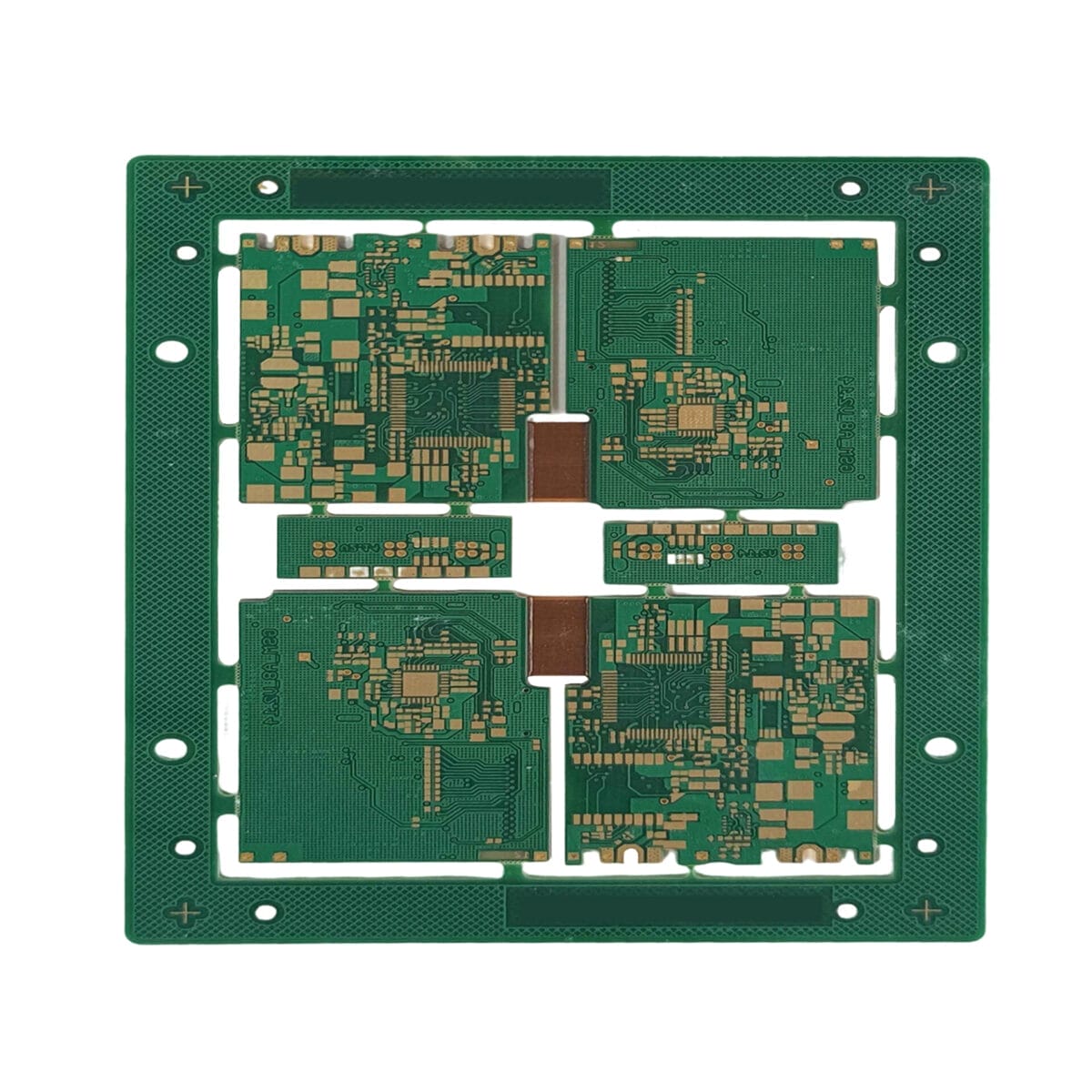
What Are the Different Types of HDI Stackups and Via Structures?
The main types of HDI stack ups include Type I, Type II, Type III, and any-layer configurations, each defined by its microvia arrangement, lamination cycle count, and routing complexity. These structures are selected based on signal density, board thickness limits, and component placement in HDI PCB design and microvia PCB fabrication.
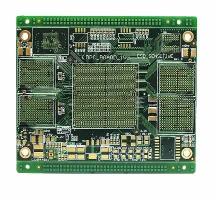
Uses a single layer of microvias on each outer layer of a rigid core. These blind microvias connect the outer layer to the first internal layer, forming the simplest and most cost-effective HDI PCB manufacturing structure for compact digital products and consumer electronics product builds.
Combines surface microvias with buried microvias in the core. This stack up supports complex BGA routing and enables high-density interconnects between internal layers. Type II designs are used in microvia PCB builds where surface area is limited and multiple signal layers are required.
Incorporates two or more stacked or staggered microvias on each side of the core, often alongside blind and buried vias. Type III supports advanced HDI builds with dense signal routing, via-in-pad configurations, and small PCB microvias across fine-pitch components.
Allows vias to connect any layer of PCB to any other using multiple stacked laser-drilled microvias and sequential lamination cycles. These structures are commonly found in high-performance devices, where routing flexibility, timing optimization, and space efficiency are top priorities.
How to Order from WellPCB Microvia PCB Supplier

Submit Your PCB Design
Upload your Gerber files or use our easy online PCB design tool to create your board layout. Make sure your files are complete and correctly formatted to ensure smooth processing and production accuracy.

Select Your PCB Specifications
Customize your order by choosing the technical specifications—number of layers, board dimensions, thickness, copper weight, solder mask color, surface finish, and more. Our intuitive interface helps you configure everything based on your project’s needs.

Get an Instant Quote
Once your design and specs are in place, you'll receive a transparent, instant quote. Pricing updates in real time as you modify options, so you can adjust your selections to match your budget before placing the order.

Confirm Order & Make Payment
Review your entire order for accuracy, including file previews and selected specs. After confirmation, proceed to secure checkout and choose your preferred payment method. You’ll receive an email confirmation with order details.

Production & Delivery
Your PCB moves into production immediately. We’ll keep you updated throughout the manufacturing process. Once completed, your boards are carefully packed and shipped to your door, with tracking information provided for your convenience.
WellPCB is trusted by millions of
businesses and innovators.


Why Choose WellPCB?
WellPCB stands out among USA PCB manufacturers by delivering superior quality, advanced solutions, and unmatched reliability. With years of experience serving global markets, WellPCB has earned a reputation as one of the top PCB manufacturers in USA.
WellPCB specializes in multilayer PCBs for advanced electronic applications. You can order these boards with $100 off using our special offer, providing high complexity at competitive rates for demanding projects.




Hommer Zhao
Founder and Chief Editor – Hommer Zhao
Welcome! I’m Hommer Zhao, the founder and Chief Editor of WellPCB. With years of experience in the PCB industry, I’m committed to making sure our content is both accurate and helpful. We’re proud to serve a growing community of over 4,000 customers worldwide, and our goal is to provide you with the best resources and support. Your satisfaction is our top priority, and we’re here to help you every step of the way!

Jesse Holland
Technical Manager – Jesse Holland
Hi, I’m Jesse Holland, an Engineer and Technical Manager at WellPCB. With years of experience in PCB design and engineering, I’m here to ensure that every project we work on meets the highest technical standards. I lead our team, focusing on precision and innovation, collaborating closely with clients to provide tailored solutions and expert guidance. Whether you’re facing a complex design challenge or need advice on technical aspects, I’m here to ensure your project is a success from start to finish.

Nathan Jensen
Purchasing Manager – Nathan Jensen
Hi, I’m Nathan Jenson, the Purchasing Manager at WellPCB. I’m responsible for sourcing the best materials and components to ensure our products meet the highest quality standards. With my extensive experience in procurement, I work closely with suppliers to secure reliable and cost-effective solutions while maintaining strong relationships to support our operations. I aim to ensure every project runs smoothly by providing the resources needed to deliver on time and to your satisfaction.

Emma
Sales Manager – Emma
Hey, I am Emma, sales manager at WellPCB. I studied electronic science and technology at university and have served customers for PCB and PCB Assembly service for several years.
I enjoy communicating with customers and our technicians to solve problems, and customers always say, "It's great to have you onboard".
It is my pleasure and honour to be helpful. Contact me now, and you'll know.

Bella and Cassiel
Sales Representatives – Bella and Cassiel
We’re Bella and Cassiel, your dedicated sales representatives at WellPCB. With our extensive knowledge of the PCB industry, we’re here to provide exceptional service and support. We take the time to understand your unique needs and are always ready to offer tailored solutions and advice. Whether you need product recommendations, assistance with your orders, or simply have a question, we’re here to ensure your experience is smooth and seamless at every step.

Mandy and Wendy
Sales Representatives – Mandy and Wendy
We’re Mandy and Wendy, your friendly sales representatives at WellPCB. Passionate about helping our customers, we bring a wealth of experience in the PCB industry to provide you with the best solutions and service. We take pride in building strong relationships with our clients, understanding their specific needs, and offering personalised support to ensure their satisfaction. Whether you’re looking for advice, product information, or assistance with any part of your order, we’re here to make your experience as smooth and efficient as possible.
Our Team
Our skilled engineers and technicians bring expertise and precision to every PCB assembly project. Committed to quality, efficiency, and innovation, our team ensures every order meets the highest UL, IPC, ROHS & REACH standards, delivering reliable solutions tailored to your needs.
- Founder and Chief Editor – Hommer Zhao
- Technical Manager – Jesse Holland
- Purchasing Manager – Nathan Jensen
- Sales Manager – Emma
- Sales Representatives – Bella and Cassiel
- Sales Representatives – Mandy and Wendy
Microvia PCB Supplier Case Studies

PCB Assembly
Advanced 8-layer HDI PCB with microvias for compact, high-density electronic designs requiring superior signal integrity.
Features:
- •Number of layers: 8 Layers
- •Surface finish: Immersion silver
- •Blind hole: L1-2, L1-3, L1-4, L5-8, L6-8, L7-8
- •Vias on Pad
- •Material: RO4003C+RO4450F
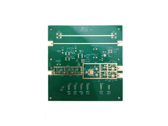
PCB Assembly
Advanced 6-layer HDI microvia PCB featuring ultra-fine pitch routing for high-performance portable and wearable devices.
Features:
- •Number of layers: 6 Layers
- •Material: RO4350B+high TG mixed pressure
- •Copper-plugged hole
- •Via on Pad
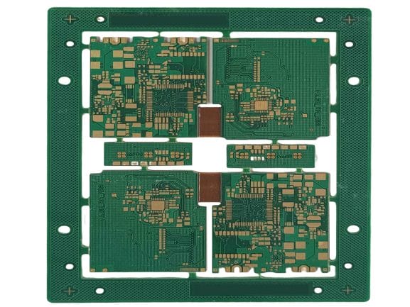
PCB Assembly
Innovative 6-layer rigid-flex HDI PCB solution delivering reliable flex-to-rigid transitions for wearables and foldable electronics.
Features:
- •Number of layers: 4 Layers Rigid+2 Layers Flex
- •Blind Vias: L1-2, L5-6
- •Line width/line spacing: 5.9mil/5mil
- •Microvia: 0.15mm
- •Blind hole process: POFV
Microvia PCB Supplier Client Feedback
As an R&D manager, I have had an outstanding experience working with WELL-PCB. For many years, our company has entrusted them with the production, assembly, and programming of the boards developed in our R&D unit, and they have consistently exceeded our expectations.
Hamid Reza Moshayedi
R&D Manager
Their work is very impressively perfect. Today, when they check our company PCB board after assemble. They found a fake short point which many engineers has never found in the past years. But that is just designed so. The PCB board quality is excellent. Their service is also excellent.
MikeZ
My friend introduced WellPCB to me, the first try, a little look forward to. I ordered a 47*72 10ps PCB, and I can’t wait to receive my PCB. So I used expedited service and received my PCB in three days. I tested and soldered the PCB, Quality is really good, silkscreen, plating also great.
Warren Cliton
Microvia PCB Supplier FAQs
What microvia diameter range do you support?
As a microvia PCB supplier, we support laser-drilled microvias ranging from 3 mil to 6 mil (75 to 150 µm) in diameter. These vias are formed using UV and CO₂ laser systems, which are calibrated for copper removal, dielectric ablation, and clean via-wall formation across HDI PCB fabrication stack ups.
What is the minimum order quantity for microvia PCB production?
We accept microvia PCB production orders starting from a single unit, allowing for the prototyping of HDI PCB designs without volume constraints. We support full scale production runs after validation, with consistent stackup, via placement and trace integrity maintained across all quantities.
Can you modify existing PCB designs to incorporate microvias?
No, WellPCB doesn’t offer PCB design services and doesn’t modify customer schematics or layouts. However, as a microvia PCB supplier, we provide DFM review for customer-submitted files and will confirm whether the existing stack up and layer configuration support microvia PCB fabrication before production.
What are the storage and handling requirements for microvia PCBs?
As a microvia PCB supplier, WellPCB recommends storing all microvia PCBs in sealed, ESD-safe packaging at 59 to 77°F (15–25°C) with minimal temperature variation. Humidity should be maintained between 45 to 65% RH in moisture barrier bags.
Boards must be kept in a clean, dust-free area away from corrosive chemicals. When stored properly in original packaging, shelf life is typically 6 to 12 months.
What documentation do you provide with completed microvia PCB orders?
Each shipment from WellPCB includes a stack up drawing, material certification, plating thickness report, microsection analysis, and X-ray inspection for blind and buried vias, laser-drilled microvias, and stacked microvias.
As a microvia PCB supplier, we also provide electrical test summaries, with impedance and RoHS documentation available upon request.
The Microvia PCB Supplier You Need for Success
Get $100 Off Your First Order!
Partner with a microvia PCB supplier who delivers high quality, ISO and IPC rated products in prototype or mass production qualities.
