Contents
What are PLCC Packages?

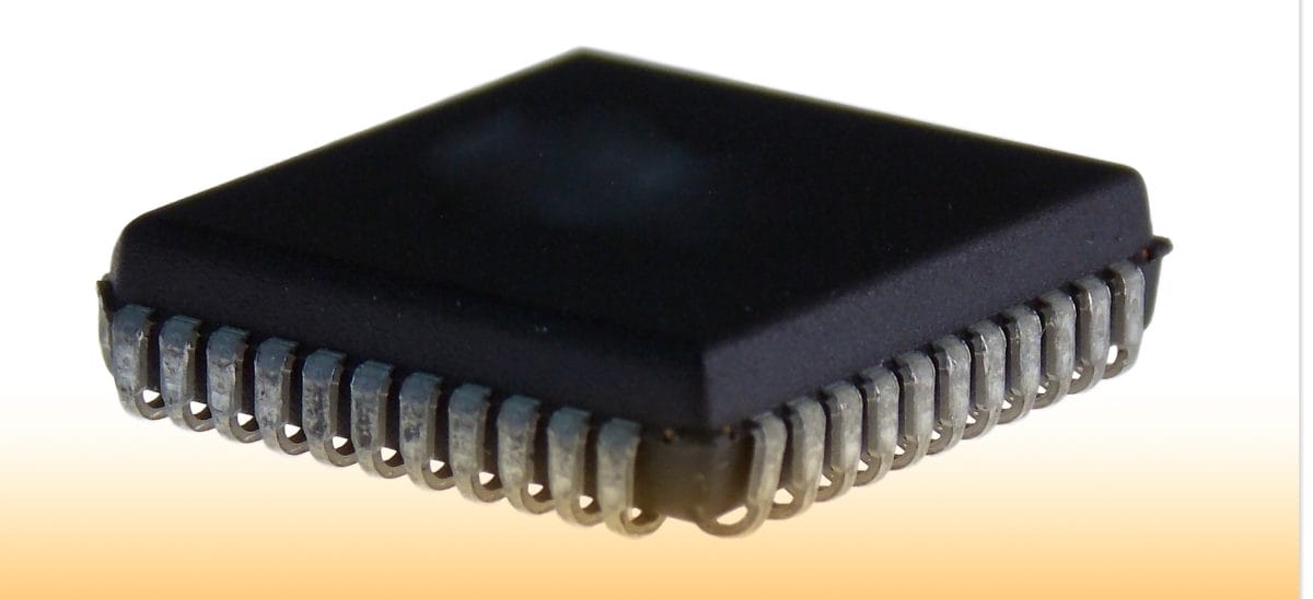
PLCC, or plastic leaded chip carrier, is a type of SMD package designed to house integrated circuits in a square or rectangular form.
Introduced in 1976 and gaining widespread use by the early 1980s, PLCCs are a cost-effective alternative to ceramic leadless chip carriers (CLCCs) and are among the most popular chip carriers today.
There are two PLCC package types:
- Square packages (MO-047 standard), introduced in 1984.
- Rectangular packages (MO-052 standard), introduced in 1985.
A defining feature of PLCCs is their J-shaped leads, which distinguish them from the gull-wing leads often found on flat-pack SMDs. This unique shape allows PLCCs to be either soldered directly onto the PCB or mounted in a socket, making them easy to replace without the need to rework the board.
PLCCs also come in two physical variants: one with a heat spreader and one without. While both are almost identical, the heat spreader variant offers better thermal performance in certain applications.
Modern PLCCs are made using environmentally friendly, lead-free materials.
In the next section, we’ll examine leadless chip carriers (LCCs) to see how they compare.
What is an LCC Package?
The leadless chip carrier (LCC) can be seen as an evolution of the PLCC. Instead of the J-shaped leads found in PLCCs, LCCs feature small pins located at the bottom edges of the package. These pins enable electrical connections without extending outward like traditional leads. LCCs can either be plastic or ceramic.
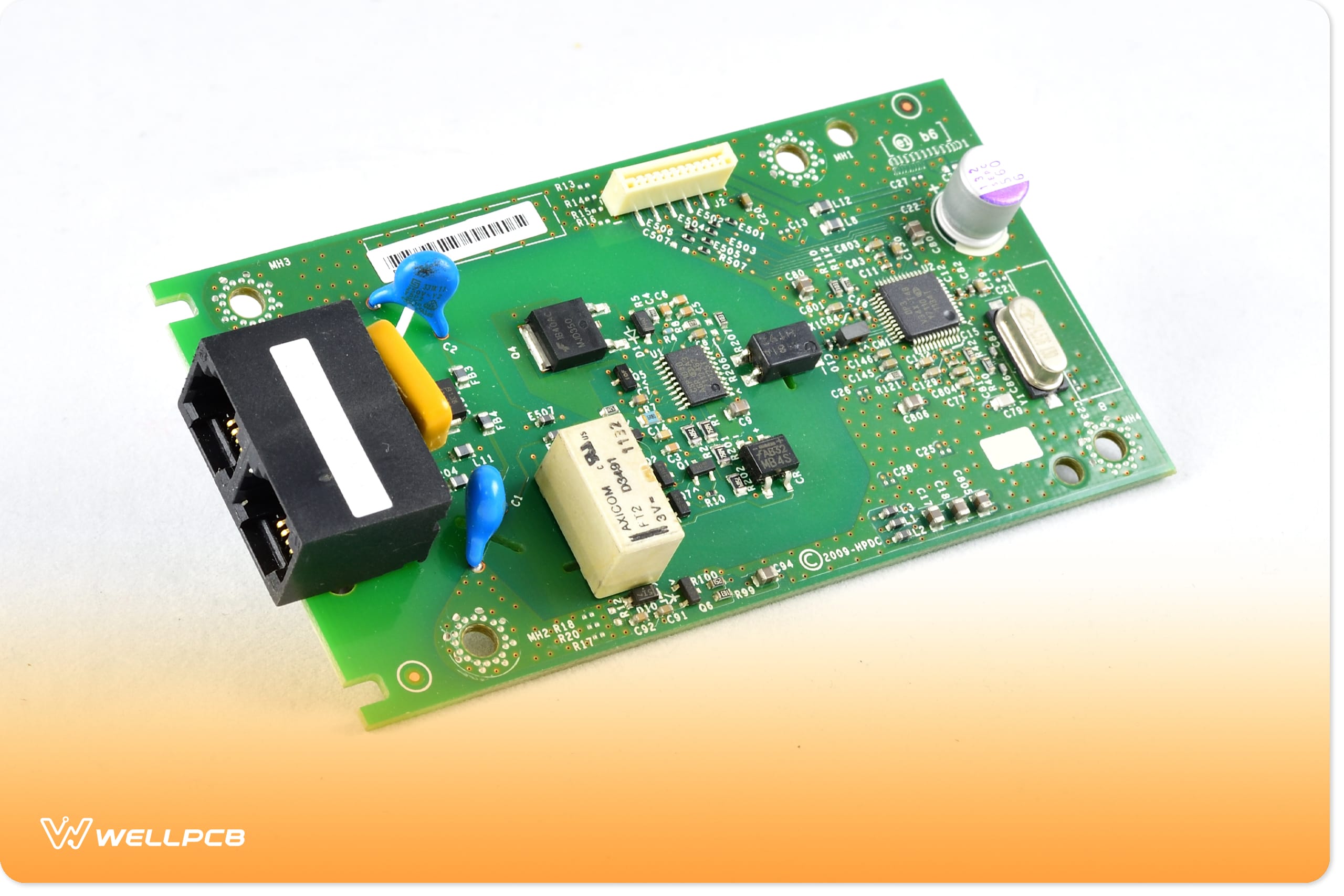
Design and Construction of PLCC Packages
PLCC packages typically have rectangular or square-shaped bodies that primarily consist of thermoset plastic. Their leads extend uniformly from all four sides, forming a J-shape that facilitates direct PCB soldering or socket mounting. Inside, the leads connect to an integrated circuit (IC) through a lead frame, a structural component that provides electrical connectivity while holding the IC in place.
The leadframe can either consist of pure copper or a blended copper alloy. Manufacturers etch or mark the top of each PLCC package. The exterior of the PLCC package is marked with key information such as the manufacturer’s name, the package’s part number, and the date of manufacture.
Types and Sizes of PLCC Package

PLCC packages come in a variety of shapes and sizes, each with different pin counts and space requirements. You can identify the specific type of PLCC package by its part number.
The most common PLCC packages and their pin counts are as follows:
Standard PLCC
Standard PLCC packages are among the most commonly used, with pin counts ranging from 20 to 84.
Thin PLCC
These packages can accommodate the same number of pins as the standard PLCC, but they have a thinner body and lower profile.
Quad PLCC
Quad PLCC packages are designed for higher-density configurations, offering between 44 and 84 pins.
Miniature PLCC
Miniature PLCCs have pin counts ranging from 16 to 52, and are intended for smaller designs with limited space.
Enhanced PLCC
Enhanced PLCCs have the same pin count as Standard and Thin PLCCs, but they feature a heat sink that helps regulate the temperature of the IC chip.
Ceramic PLCC
The Ceramic PLCC is a variation of the standard PLCC that replaces the plastic body with a ceramic one. This enables better heat management, making it more suitable for high-temperature environments.
PLCC vs. LCC Packages
The main difference between these PLCC and LCC packages is that the PLCCs have leads while LCCs do not. Instead, LCCs use recessed metal pads along their edges to make electrical connections.
LCCs are popular because they are lightweight and versatile. They are especially useful for mounting and unmounting ICs, like microprocessors, without permanently soldering them to the PCB. This makes them a good choice for testing or applications where components need to be replaced often.
Both PLCCs and LCCs are available in square or rectangular shapes and can be made from plastic or ceramic. However, LCCs cannot be soldered directly to the board, while PLCCs offer more flexibility by allowing both soldering and socket mounting.

How to Troubleshoot and Repair PLCC Packages
The small size and compact design of PLCC packages can make troubleshooting and repairs tricky. Their tightly packed pins and integrated circuits make it harder to find faults, especially if the package has already been soldered to the PCB. However, following these steps can help:
- Visual Inspection: First, visually inspect the PLCC and its connections. Look for discoloration, cracks, or leaks on the package. If the package is soldered to the PCB, check the solder joints for damage or breaks. Make sure the leads aren’t bent or broken.
- Inspect and Test the IC: If the package looks fine, test the IC to ensure it’s working. A multimeter is a common tool for this and can help you identify any internal issues without removing the package.
- Replace the PLCC package: If the IC works and the connections seem intact but the problem remains, you may need to replace the package. This will require you to carefully desolder the faulty PLCC from the PCB and install a new one.
It’s always best to consult a professional when working with electronic components for advanced circuits—especially if you’re a novice.

Pros of PLCC Packages

PLCC packages offer several benefits that make them a popular choice in certain electronic applications:
- PLCCs are more cost-effective, as they’re cheaper to produce than ceramic leadless chip carriers (CLCC).
- PLCCs can be soldered directly to the PCB or mounted in a socket, allowing for easy replacement and repair.
- If the PLCC contains a programmable logic device (PLD), it can be programmed and tested independently before being connected to the board.
- This allows you to test and troubleshoot the system, especially when onboard programming is unavailable.
- The J-shaped leads fold inward, making PLCCs more compact than packages with outward-folding gull-wing leads, like those in QFPs.
- Mounting in a socket eliminates the need for soldering near the IC, protecting it from potential heat damage.
Cons of PLCC Packages
While PLCC packages have notable advantages, they also come with a few drawbacks:
- The small size of PLCCs restricts the number of available pins, which can limit their use in more complex designs.
- Compared to BGAs and QFPs, PLCCs are less efficient at dissipating heat, reducing reliability in high-temperature environments.
- Long signal paths and fewer pins result in slower signal speeds, making PLCCs less suitable for high-performance applications or those requiring high speeds.
In Summary
This guide explored the features, advantages, and limitations of plastic-leaded chip carriers, defined their advantages, and compared them to leadless chip carriers. With this knowledge, you should be in a better position to determine the best surface-mount device for your PCB.
We hope you enjoyed reading this guide and found it helpful. As always, thank you for reading.
At WellPCB, we specialize in PCB fabrication and assembly, including expert handling of IC packages like PLCCs. Contact us today for reliable, high-quality solutions tailored to your needs.