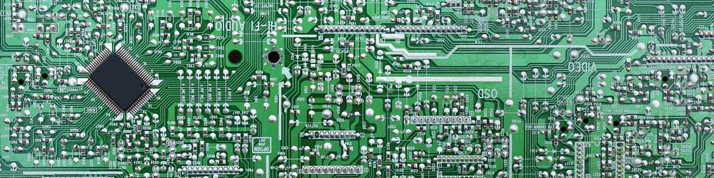
Recent developments in consumer electronics have heightened the need for producing defect-free PCBs. It is significant to understand the issues encountered when transitioning from the design phase to the production phase. During the production phase, defects, like wrong solder joints and misalignment, may happen, accentuating the need for methods to check defects on soldering PCB board.
To understand what it takes to produce defect-free PCBs, this article introduces you to the common types of soldering mistakes and the practices to effectively recognize the soldering flaws.
Contents
1. Identifying Common Types of PCB Soldering Defects
The production process of PCB includes screen printing, component placement, and soldering. This section of the article is going to familiarize you with different types of soldering defects. We are going to briefly describe each PCB soldering issue along with its causes and solutions.
1.1 Soldering PCB Board—Pinhole
Description:
A pinhole or blowhole is a small hole formed in a joint soldered on PCB to mount a component using through-hole technology. We can use the term pin and blow interchangeably; however, it is common to use a pinhole to indicate a smaller hole size. You can identify pinholes or blowholes by the thick copper plating formed during the process.
Causes:
The moisture and volatiles that leak through the vacuums in the copper plating are the leading causes for the pin and blowholes.
Solution:
We can solve this problem by using a higher quality board with at least PCB copper thickness.
1.2 Solder bridging
Description:
Solder bridging is one of the most challenging soldering defects to discover because we can’t recognize it by the naked eye. Solder bridging form short circuits, which can lead to serious harm to the PCB circuit. This type of error occurs when soldering crosses mistakenly connect two leads.
Causes:
Common causes of solder bridging are wrong PCB stencil specifications leading to an excessive amount of solder on the pads, failure to match the PCB stencil with the board, and misplacement of components.
Solution:
The solder bridges can be fixed using a desoldering wick. You can repair this defect by applying the wick on the soldering crosses, and then, with proper heating, the extra solder will be removed.
1.3 Tombstoning
Description:
Tombstone refers to a soldering defect when one of the component terminals fails to stay attached to the board while the other stays coupled to the board. Small components are more likely to have this issue during the soldering reflow procedure.
Causes:
The main reason for this issue is the unequal wetting power throughout the reflow. The exterior tension between the PCB pad and the liquid solder may misplace the components, especially for small and light ones.
Solution:
The tombstoning issue can be fixed by refining the precision of stencil printing and ensuring that the pick and place nozzles have a suitable pressure to deal with small components. You can decrease the chances of tombstoning by slowing down the component placement process to increase accuracy. Also, you have to double-check that the pad dimension design agrees with the datasheet.
1.4 Soldering PCB Board—Uneven hole fill
Description:
Bad fluxing or heating results in uneven hole filling. As its name implies, this issue occurs when the soldering fails to fill the through-holes.
Causes:
Uneven hole fill usually happens when the preheating process is not long enough or the flux is not applied correctly.
Solution:
You have to increase the healing process to attain the topside temperature. We can solve this issue by modifying the preheating settings. It would help if you also considered a more extended wave contact time to overcome this problem.
1.5 Overheated joints
Description:
You may come across overheated joints when the heating process cannot melt the soldering wire, leading to overheated flux on the pad. It is hard for us to repair this defect because of the overheated change.
Causes:
Despite the heating process, the solder fails to flow in the joint.
Solution:
Clean the overheated flux from the joint by applying isopropyl alcohol, then use a suitable brush to remove the change.
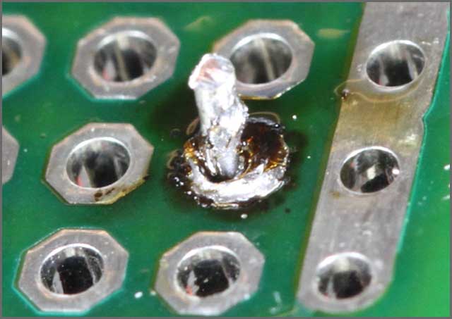
1.6 Soldering PCB Board—Cold joints
Description:
In contrast to overheated joints, cold joints appear when the heating fails to melt the solder fully. We can distinguish cold joints by its rough surface, and it is vulnerable to cracks.
Causes:
Insufficient heating or using an excessive amount of soldering.
Solution:
Apply suitable heating to the cold joint until the excessive solder is fully molten.
1.7 Flux residues
Description:
We recognize this defect by flux residues formed on the PCB board because of contamination.
Causes:
The flux and poor cleaning conditions cause the residues to be formed on the pad.
Solution:
Using no-clean low residue wires and materials can significantly reduce flux residues.
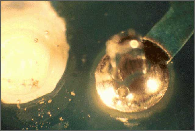
1.8 Excessive solder
Description:
Applying an excessive amount of solder is not a good idea as it may result in short circuits and unreliable connections. The best practice is to use just a sufficient amount of solder to connect the components’ terminal with the pad. We detect this defect by searching for the bowl-shaped surface areas on the joints.
Causes:
Using an unnecessary extra amount of soldering in the joints
Solution:
Fixing this defect should be comfortable and straightforward. Melt the excess solder with the soldering iron and remove it with a solder sucker.
1.9 Soldering PCB Board—Insufficient solder
Description:
Unlike the previous one, we face this issue when insufficient soldering to connect the joints, resulting in connections failure and open circuits.
Causes:
Insufficient amount of soldering in the joints.
Solution:
Add additional solder to the defected joint to ensure reliable contact.
1.10 Solder skips
Description:
We encounter this defect when soldering a joint, entirely skip from the process. Unfortunately, this leads to open circuits and functional failure of the PCB.
Causes:
We are most likely to encounter this defect when we have the wrong component dimensions and flux gassing.
Solution:
Carefully revise your PCB specifications to ensure the correct placement of the components on the board.
2. Soldering PCB Board—Testing methodologies for Soldering PCB Board issues
Manufacturers use different types of tests to identify PCB defects. In this section, we are going to discuss the micro-sectioning analysis test and solder-ability analysis test.
2.1 Micro-sectioning Analysis
Micro-sectioning is used to check the performance of processes that produce through-hole PCB boards. It is a destructive method because it depends on exposing a cross-sectional view of the PCB; however, this test provides us with an accurate way to identify solder reflow failures.
2.2 Soldering PCB Board—Solder-ability Analysis
A Solder-ability test is always employed to verify PCB surface robustness and ensure that solder joints are reliable. This technique tests the capability of the board to be wetted by molten solder. We confirm that the components will meet the standard requirements and verify that storage has no adverse effect on the boards’ capacity to solder.

3. Soldering PCB Board–Preventive Soldering Practices
Better safe than sorry! In this section, we are going to explore the best methods to prevent soldering defects effectively. To recognize and solve common soldering defects e design to the manufacturing and brand unnecessary extra expenses to finalize the PCB board.
Soldering PCB Board–Pinhole:
- The best practice to prevent pinholes and blow holes is to bake the PCB just before the soldering process.
Solder bridging:
- Use the correct PCB stencil specifications.
- Make sure to use the correct reflow profile.
- Pay attention to the component placement by applying appropriate pressure.
- Make sure that the stencil apertures place is matched with the pad.
Tombstoning:
- Revise the pad dimensions for the small components.
- Consider using anti tombstoning soldering paste.
- Correct the stencil specifications.
- Examine the placement and routing process and make sure that all traces have equal widths.
Soldering PCB Board–Uneven hole fill:
- A good rule of thumb is to maintain the topside temperature to be between 100 and 110°C for double-sided boards and use a temperature slightly below this threshold for single-sided boards.
Overheated joints:
- Before every time you start the soldering process, make sure to preheat the iron sufficiently. Also, cleaning the joint before soldering will avoid you facing this issue.
Soldering PCB Board–Cold joints:
- Preheating the soldering iron will prevent this defect from happening.
Flux residues:
- Proper preheating can reduce the flux residues on the PCB board. It is also affected by the contact time of the wave.
Solder skips:
- Contact your manufacturer and make sure that the right wave height between the board and soldering wave is used.
Conclusion
Achieving a successful transition from the PCB design phase to the manufacturing phase depends on minimizing the soldering defects as much as possible. The article’s primary goal is to familiarize you with the common types of PCB soldering defects and how to identify these defects. We discussed common soldering issues and the testing, repairing, and preventing procedures for these PCB soldering problems.
We can fix the most common soldering defects; however, it is strongly recommended to follow preventive measures to avoid such defects and issues in the soldering process. Now, we hope that you can distinguish between different types of faults and follow preventive soldering actions.
Please see ‘ Surface Mount Troubleshooting Guide for further information to help identify Soldering PCB Board defects, understand causes, and what preventative actions can be taken.