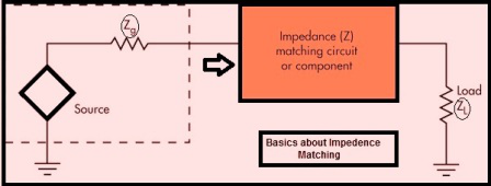
Matching Impedance is a characteristic of Radiofrequency or microwave design. An impedance of 50 ohms is required to effectively transmit the signal’s power from input to destination loaded with minimum distortions.
Suppose the impedance does not match at input and output. There can be a signal loss, power cannot be transferred to production, or distortion may arise, leading to vertical waves. That ratio can approach infinity.

1. Introduce
But if Matching Impedance is matched. Then the problem of distortion or standing waves cannot occur. Or it can be a low vertical wave fraction in terms of voltage.
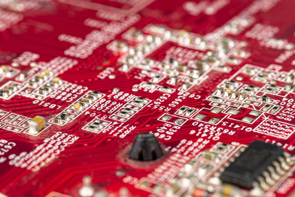
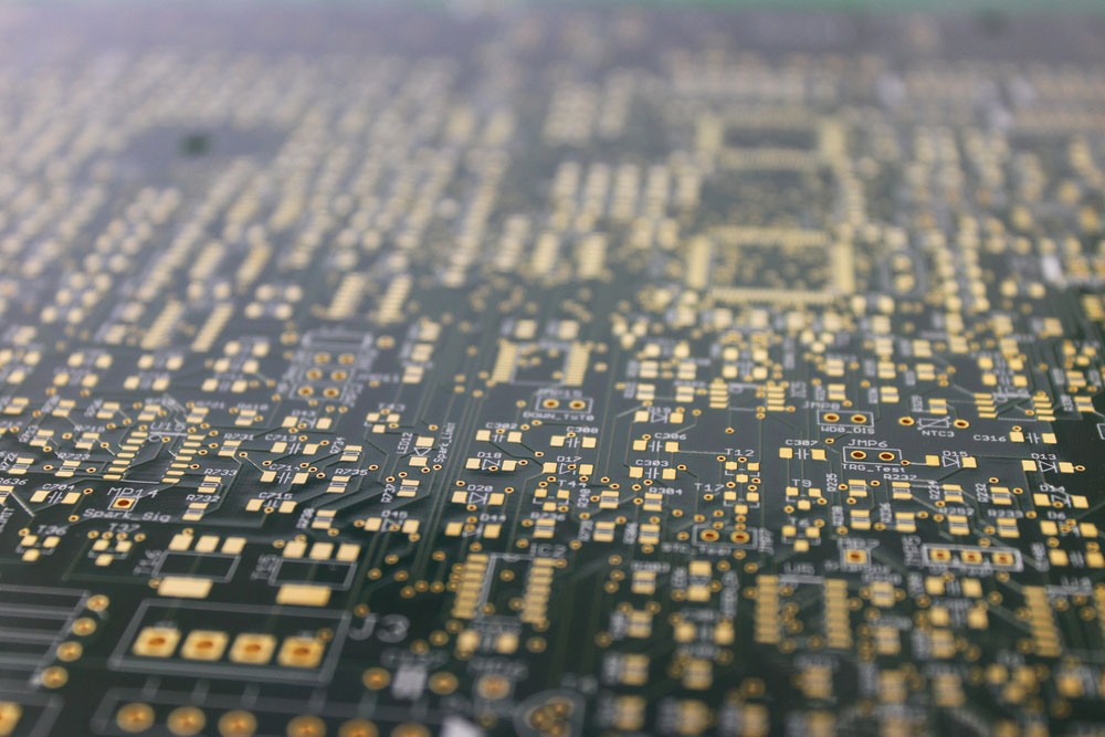
But it is not easy to maintain an impedance equal to 50 oms during transmitting a signal from input to output. To uphold the impedance, Stripline or microstrip technologies are used.
It displays that impedance of the transmission line is contrarily relative to the line girth. Corresponding to the wideness of the substantial dielectric layers.
One contrast between microstrip and Stripline is that. The stature of the flag following over the ground for Stripline has less of an effect on impedance.
It is more effective than the stature of a microstrip flag following over the floor. The air above a microstrip schematic will contribute to the specific impedance.
It displays the impedance of the transmission line. As contrarily relative to the line girth. And explicitly corresponding to the perimeter of the substantial dielectric layers.
If the circuit, while a stripline schematic is confined to the interior. That of a sandwich of dielectric material. Air will constantly work to lower the operating dielectric constant of PCB solid. It is used in a microstrip schematic.
Due to this condition. The operative dielectric constant of PCB components is used in a stripline schematic. It will be greater than the dielectric constituents used in a microstrip schematic.


2. Matching Impedance—Conclusion
By the wideness of the metal conduit layer utilized for the transmission lines. The size of the flag-shaped on that layer. And the wideness of the dielectric substrate. Smith’s chart is used to acquire an impedance matching.