
If you have worked with the PCB, you have noted the copper layers running from one point to the other. But have you ever wondered if its thickness matters? Well, if you have, this article is tailormade for you.
Read on to understand the basics of track width and its essence in PCB boards.
Contents
What is track width?
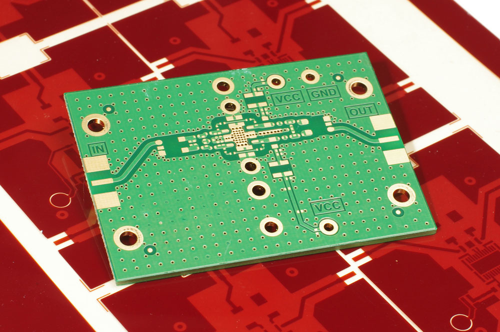
Fig 1: A PCB showing the traces
The track is the active layer/ conductive path of copper trace connecting one point to another on a PCB. You may also find it called the PCB trace. Meanwhile, the track width is directly proportional to the thickness of the copper track.
Typically, you’ll find track width given in millimeters (mm). Also, the parameter is essential in determining the board’s pattern class.
An ordinary signal layer will transmit efficiently in a track width value of approximately 0.150milimeters or 6mil.
Trace width Calculation

Fig 2: You can calculate the PCB’s trace width
Note that the PCB thickness trace operates as a resistor. Hence, the narrower and lengthier it is, the higher the resistance. We will illustrate how to deduce the trace resistance and the PCB trace width.
First, you can calculate the allowable current via this formula.

I is the Electric Current, Delta T is the temperature change, while A is the track’s cross-sectional area. Therefore, rewrite the above equation for track width and make the cross-sectional area the subject of the formula. Here is the final equation after the rearrangement.

Lastly, you can now calculate the PCB track width via the equation below.

Remember, the above formulas are applicable in tracks with 0 – 35 Amps current and a temperature change of between 10 and 100 degrees celsius.
Track width Design Tips

Fig 3: You need to maintain a particular minimum track width
You should be guided by the design specification and the current to pass through the tracks during the design process.
But, always ensure that you have a minimum route track Width of 1.0mm per Amp. Such width will be the best fit for a copper thickness of 1.0oz/ft2. Ideally, copper trace in most PCBs has this thickness.
However, due to particular application conditions, you may not go for this width in some cases. Using a track width calculator would be of immense help in such scenarios. Also, during design, ensure that the width isn’t too broad that it interferes with nearby traces to prevent short-circuiting.
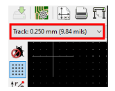
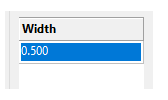
Kicad Track Width: How to change?

Fig 4: You can change the Kicad Track Width from the settings
Version 5.1.8 KiCad has a default trace width of 0.250 millimeters or 9.84mils. While it is still a viable width, it’s relatively thin and likely to break. Hence, an additional copper thickness is necessary. Ideally, we can expand it to a width of approximately 0.500 millimeters or 19.69mils.
Such thickness is ideal for power load transfer and signal traces.
However, you can still go below this value if your – tool – design demands. Just don’t go below the default 0.250mm.
Here are the key steps for altering the track PCB thickness:
Click on “PCBNew” and select the width-changing dropdown.
Then, choose edit “pre-defined sizes.”

Next, select “Track and Vias” in the subsequent window, and from the column, click the + button.

You will be prompted to input a figure. Write 0.500 and key in “Enter.”
Lastly, confirm if you have entered the right layer-specific values by checking the width dropdown. If you did everything correctly, it should display on the dropdown.

Note that the KiCad can sometimes switch back to the 0.250mm value. Thus, stay vigilant and change the value anytime it alters.
Also, check out the difference in the Cu-Foil thickness from the diagram below.


Conclusion
We have provided a systematic review and meta-analysis of track width. Thus, you’re now good to go in this discipline. For more information on this topic, simply reach out.