Do you deal with many power switching applications, or do you need an electrical device and PCB component that has a wide application? Then, the TRIAC is the ideal option. That said, the TRIAC symbol is another aspect worth looking into since it’s the circuit symbol that indicates bidirectional properties. If you’re new to this, you don’t have to worry. In this article, we’ll break things down by explaining what it is and how it works. We’ll also touch down on the detailed explanation of TRIAC symbols, the TRIAC application, construction, and much more.
Are you ready? Let’s get down to business
Contents
What is TRIAC?
TRIAC is an acronym that you can split into two. That is, the TRI stands for triode while the AC means alternating current. In other words, the TRIAC is a three-terminal electronic component. And it can regulate the voltage in both directions when you activate it.
You can also define the TRIAC as a semiconductor device with three terminals and four layers that control AC variable power.
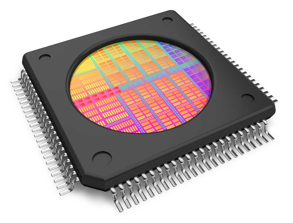
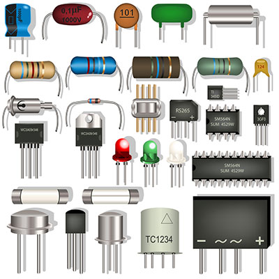
An example of a Semiconductor device (a microchip with a die)
Aside from the acronym or term being a generic trademark, it’s also a subset of thyristors similar to the regular relay. That is, a small current and supply voltage can regulate a way bigger leakage current and voltage. Also, the TRIAC is similar to SCRs. SCR means silicon-controlled rectifiers. And it relates to the TRIAC because they both allow voltage flow.
Also, they both conduct current continuously, especially if the gate current stops. So, they only stop conduction when there’s a holding current (the main current).
What’s the difference between both electrical components? With the silicon, you need a positive voltage to trigger it while the TRIAC requires either a positive or negative voltage. Plus, the SCR is unidirectional while TRIAC is multidirectional.
In short, the TRIAC is a convenient switch for alternating current thanks to its bidirectionality. Also, when you trigger the controlled AC phase angle attached to the main circuit, it automatically allows regulation of the normal voltage flowing into the phase control or load.
Further, you can use bipolar power electronics and power supply devices for regulating the velocity of dimming lamps, universal motors, electric heaters, etc.
TRIAC Construction
Like we mentioned earlier, the bidirectional device has three terminals and four layers. So, its construction involves two SCRs. Thus, both SCRs connected in inverse parallel alongside a common gate region terminal in one chip device.
Also, the terminal semiconductor device has six doped regions. Plus, it has a gate circuit terminal G that has ohmic contact with the P and N materials. As a result, the gate terminal can allow the trigger pulse of either polarity to begin conduction. The term Cathode and Anode gate control input don’t apply in this construction since the TRIAC is a bilateral device.
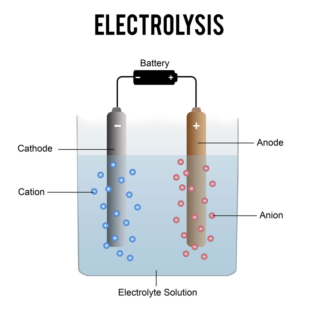
Electrolysis process describing cathode and anode
So, you can label the terminals as main terminal 1 (MT1), main terminal 2 (MT2), and extra gate G.
How Does a TRIAC work?
The best way to understand the bidirectional device operation is by triggering each quadrant. Also, it’s important to note that the physical structure of a particular TRIAC affects the relative sensitivity.
Quadrant 1
The operation usually begins in the first quadrant when MT2 and the gate are positive—for MT1. That is, the current from the gate makes a corresponding NPN transistor come on. As a result, it pulls current from the bottom of a corresponding PNP transistor, which also puts it on.
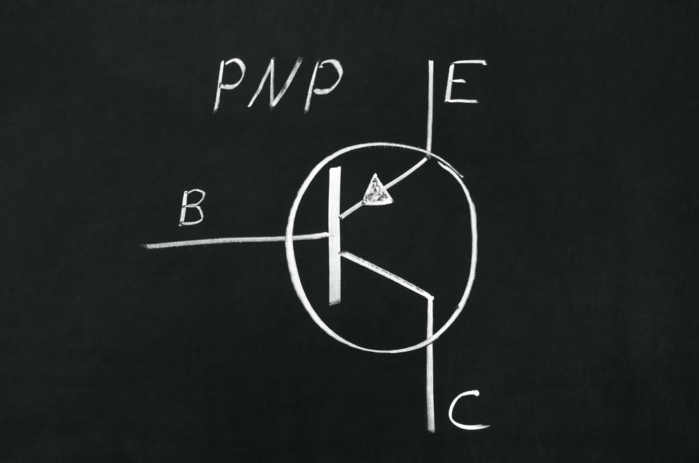
A symbol of the PNP transistor
Some of the dotted line or gate buffer current is lost via the ohmic path along the p-silicon. Then, it flows straight into the MT1. And it does this without running through the NPN transistor base. When this happens, the injection of holes in the p-silicon allows the stacked layers (n, p, and n) under MT1 to act like an NPN transistor—which switches on because its base has current.
Also, it affects the p, n, over MT2 as they act like a PNP transistor that comes on due to its n-type base. Plus, the base turns forward-biased with its emitter (MT2). Hence, the triggering scheme is similar to an SCR. This quadrant is pretty sensitive because it lies where the gate current injects into the base of the primary device transistors.
Quadrant 2
Operation in the second quadrant happens when MT2 is positive and it has a negative gate for MT1. When the device turns on, it happens three-fold. And it begins when the voltage starts flowing inside the gate from MT1 via the p-n junction under the gate. Hence, it switches on a structure that comprises an NPN transistor and a PNP transistor—which sees the gate as a cathode.
So, as the current flowing inside the gate increases, there’s a chance that the p-silicon’s left side beneath the gate resistor rises to MT1—because the difference between the MT2 and gate tends to reduce.
As a result, a current establishes between the right and left sides of the p-silicon. Then, the current switches on the NPN transistor beneath the MT1 terminal. Also, the same thing happens for the PNP transistor in the middle of the upper p-silicon’s right side.
Finally, where the major part of the voltage crosses the structure is identical with the quadrant 1 operation.
Quadrant 3
The operation in the 3rd quadrant happens when the MT2 and gate are negative to MT1. It begins in the number one phase. And it happens exactly when the PN junction in the midst of the gate and MT1 terminal gets forward-biased. So, it means there’s an inclusion of minority carriers. This action happens in both the layers that join the junction. So, electrons inject in the player beneath the gate.
However, not all the electrons recombine. Hence, these electrons move to the lower n-region. The second phase involves lowering the prospects of the n-region. Then, it acts as the PNP transistor’s base switches on directly. Also, the voltage of the player increases and it acts as the collector of the PNP transistor above the MT2 terminal. Then, it gets activated.
Quadrant 4
The fourth quadrant operation happens when the voltage of MT2 becomes negative to MT1 and the gate voltage is positive. The process of triggering this quadrant is the same as the third quadrant. You can start by using gate control. When the current moves from the player beneath the gate into the n-layer, minority carriers move into the p-region.
So, some of the free electrons travel into the n-region without remerging. In short, the process continues in the same pathway as quadrant 3. Afterward, the current reaches the last conduction path.
Additionally, this quadrant is less sensitive than others. Plus, some snubbers and logic-level types of TRIACs don’t trigger in the quadrant—it only activates for the extra three quadrants.
TRIAC Symbols
The TRIAC symbol is a simple circuit diagram that combines two equal SCRs in inverse parallel to each other. Also, the gates of the two SCR merge to form a single gate. And there won’t be any current flow except there’s you inject a gate current pulse at G.

TRIAC Symbols– TRIAC Application
No doubt, the bidirectional device appears to be one of the most widespread electrical components of the thyristor family. And you can find them in some power applications like:
- Electric fans

Image of Electric fan
- AC power control
- High power lamp switching
- Light dimmers

Electric light dimmer switch
- Electric motors
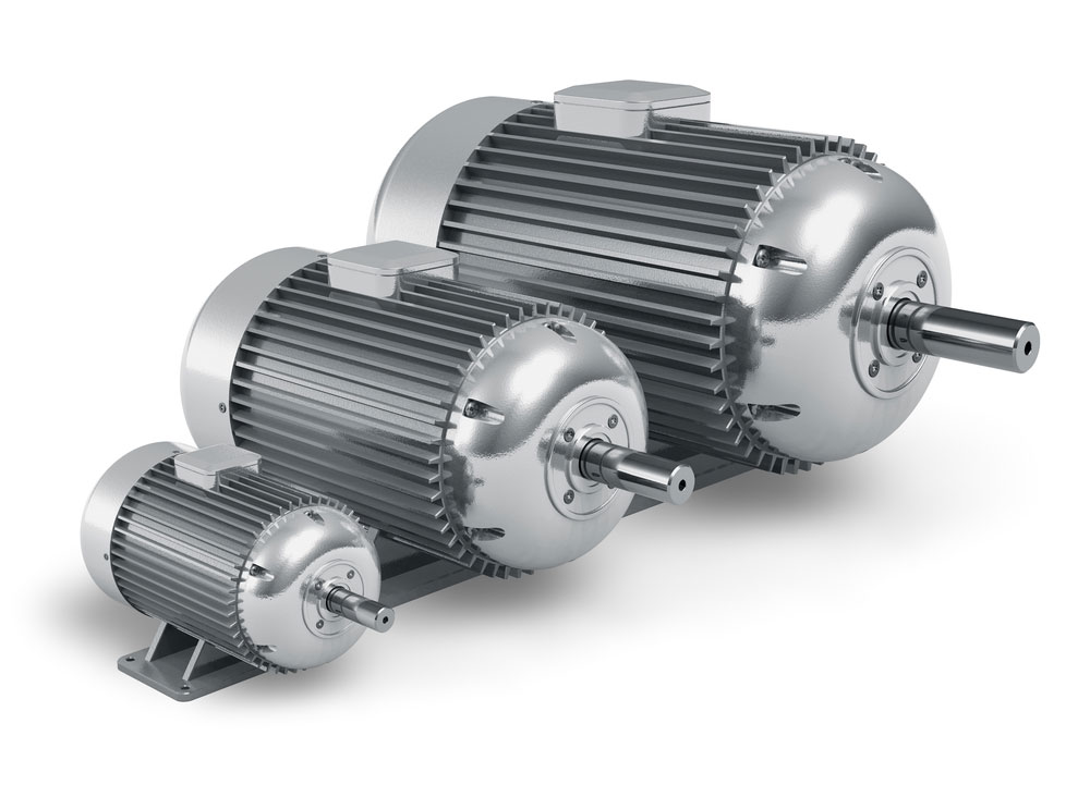
A set of electric motors (Industrial)
TRIAC Symbols– Characteristics of TRIAC
There are four major modes that the characteristic curve of a TRIAC holds:
- Mode 1: This happens when the first quadrant operates. So, VMT21 and VG1 are positive
- Mode 2: the second quadrant operates here. Hence, the VMT21 is positive while VG1 is negative.
- Mode 3: in this mode, the third quadrant operates. Therefore, VMT21 and VG1 are negative
- Mode 4: this is where the fourth quadrant operates. Thus, VMT21 is negative and VG1 is positive
Where:
- VMT21 – voltage of terminal MT2 to terminal MT1
- VG1 – gate voltage to terminal MT1
The current and voltage values of a regular TRIAC are:
- Holding current – 75mA
- Average triggering current – 5mA
- On-state current – 25A
- On-state voltage – 1.5V
TRIAC Symbols– How to Test a TRIAC
You can test a TRIAC with an ohmmeter or multimeter in the following steps:
- Ensure that the multimeter is in ohmmeter mode
- Confirm the charge of the ohmmeter lead by using a junction diode
- Link MT1 to the negative lead and the MT2 to the positive lead
- Join the gate of the TRIAC to MT2 with a jumper lead
- Ensure that the multimeter shows no continuity via a TRIAC. And you can do this by reconnecting the TRIAC. That way, MT1 will connect to the positive lead and MT2 to the negative lead
- Link the gate again to MT2 with a jumper lead. And the ohmmeter should show a forward diode junction
TRIAC Symbols– What is The Difference between DIAC and TRIAC?
First off, DIAC (diode alternating current) is an inverse parallel combination of two diodes. The TRIAC on the other hand, is an inverse parallel of two SCRs—and their gates merge to form the TRIAC gate.
Second, TRIAC has three terminals, while DIAC has two terminals. Thirdly, the power handling capacity of TRIAC is higher compared to DIAC. Also, you need to apply a negative or positive voltage at the gate terminal to initiate a TRIAC.
But you can trigger a DIAC by adding a voltage across its terminals—equal to or more than its break-over voltage.
Lastly, TRIAC has a gate terminal, unlike DIAC that has none.
Final Words
TRIAC symbols are quite easy to understand since the illustration is simple. And the TRIAC has its good side. For instance, it requires a single fuse for protection, and the device has a safe breakdown in either direction. In short, the three-terminal, bidirectional semiconductor is effective for controlling AC power.
So, what do you think about the topic? Do you plan to use it for your next ac power-related project? Or do you have questions and suggestions? Please feel free to reach out.