
Contents
Ball Grid Array (BGA)
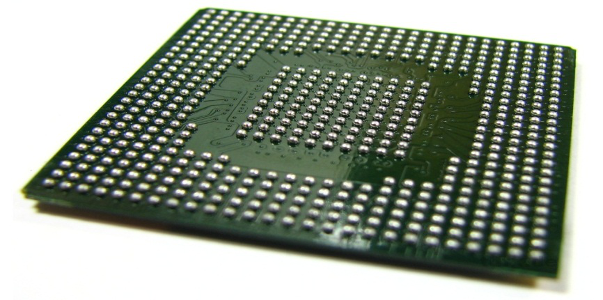
Ball Grid Array (BGA) refers to a particular type of surface PCBA used to permanently mount devices, such as microprocessors, to printed circuit boards. A BGA has several advantages over other methods, and as such, it has become a popular technique used in manufacturing integrated circuits and electronic devices.
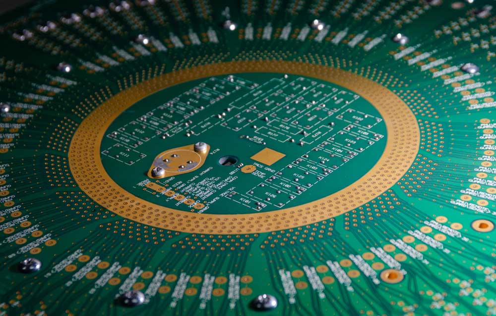
A common form of electronic manufacturing is ball grid arrays derived from pre-existing pin grid array (PGA) technologies. Instead of utilizing pins to conduct electrical signals from the circuit board, a ball grid array uses tiny drops of solder.
These solder balls are placed evenly apart on the board in an array of symmetrical grids and gently heated in a specialist oven. Surface tension ensures that the components are kept in position.

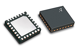
Quad Flat No-Lead (QFN)
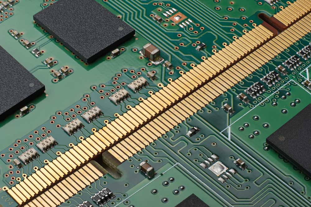
The QFN (Quad Flat No-lead) package is probably the most popular semiconductor package today for four reasons: low cost, small form factor, and good electrical and thermal performance.
Like any other semiconductor package, a QFN package functionality is to connect (both physically and electrically) silicon dies (the ASIC) to a printed circuit board (PCB) using surface-mount technology. QFN is a lead frame-based package called CSP (Chip Scale Package), which can view and contact leads after PCBA.
The QFN can have a single or multiple rows of pins. The single-row structure is formed either by a punch singulation or a saw singulation process; both methods divide various packages into individual packages. The multi-row QFN uses an etching process to realize the wanted number of rows and pins; these are also singulated, typically by saw.
The benefits of choosing the QFN packages include a decreasing lead inductance due to optimally short bond wires, lightweight, thin profile, and small-sized “near chip-scale” footprint. Moreover, thanks to the exposed copper die pad, the QFN is perfect for many new applications that need a better size.
LPKF
Solder resist with LPKF ProMask and PCBA prints with LPKF ProLegend.
Solder Resist Masks, and PCBA Print for In-House Prototyping Solder resist is a fundamental requirement for soldering certainty – especially for SMT. Professional quality solder resist masks can quickly and effectively be applied to structured PCBs using the LPKF ProMask. The solder resist mask is printed onto transparency from the CAD program, transferred onto the PCB, and developed. The structured PCB is given a perfect surface finish for soldering without short circuits in four simple steps. PCBA print uses a similar process. ProMask and
ProLegend includes all the tools and materials required for perfect results.
LPKF ProMask and LPKF ProLegend are essential tools for quick, easy, and inexpensive PCB prototyping or small batches. A photo-optical exposure process transfers all structures or legends onto the PCB in just a few steps.
LPKF ProMask and ProLegend Provide Professional Finishing in Four Simple Steps:
1. Print photo template
The photo template with the desired layout is printed onto a
transparency using LPKF CircuitPro and a standard laser printer.
2. Apply paint
Mix the solder resist from the pre-proportioned paint and hardener.
Apply the solder fight onto the structured PCB with the included roller.
The PCB is then pre-dried in a convection oven for 10 minutes.
3. Expose photo template
Position the photo template on the PCB and place both in the UV exposer.
Activate the laser setter for 30 seconds. Remove the PCB and remove the
photo template.
4. Develop and harden solder-resist mask
Prepare the developing bath with the newborn powder and hot water.
Use a brush to release the unexposed solder resist in the developing
bath. The solder resists, then hardened and cleaned in a convection oven
for 30 minutes. A powder pH conditioner then neutralizes all chemical
components for eco-friendly disposal.


