In our daily lives, digital communication has come to play an important part. The Motorola CD4012, for example, is playing a vital role in solving the day-to-day issues in the home and office-calling needs. Its digital answering machine and low energy consumption give you many features. As a result, the CD4012 is one useful logic chip that adds an edge to technology development.
The CD4012 is also helpful in other electronic fields not limited to people involved in everyday calling. Furthermore, this IC is useful for building high-end techs-like logic inverter circuits or buffer circuits. Subsequently, we explain all there is to this logic chip and its uses.
Contents
CD4012 Pinout Configuration
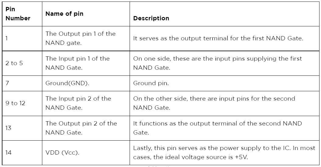
The CD4012 is a logic IC built on CMOS technology. Inside, there is a dual package of 4-input NAND gates. In other words, the IC uses two independent NAND gates that accept four logic inputs.
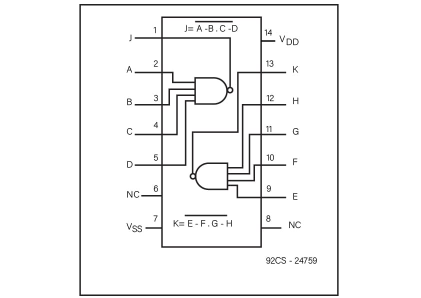
Source – Wikicommons
(Image showing the pinouts on the CD4012).
Find below a table describing each pin’s name and number.
Features/Technical Specifications
CD4012 has certain features that make it unique. Therefore, when using the CD4012 for your next project, here are the specs it offers.
- Typically, the IC comes in a dual package of OR gates with four inputs.
- For most, the ideal operating voltage is 5V. However, the voltage range of operation is between 3V and 15V. There is a high-voltage type of 20v
- The power dissipation is about 500mW.
- The minimum low voltage when at +5V is 0.05V
- On the other hand, the high voltage at a minimum is 4.95V
- The maximum propagation delay at 5V is 50ns.
- Finally, CD4012 has 14-pin packages of PDSO, GDIP, PDIP, and DIP package types.
Additionally, you can check the CD4012 datasheet for more information. Download datasheet here.
Other Development Boards Download Datasheet
Sometimes, the CD4012 logic IC might have some limitations. In such cases, there are other CD4012 development board equivalents. These equivalents include:
- 74HC20
- 74HCT04
- 74S140
- 74LS00
- 74LS02
- 74LS08
- 74LS04
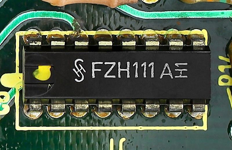
(Image of the FZH111, which is a suitable alternative to the CD4012)
Where to use CD4012 IC?
There are incredible features this programmable IC offers to digital devices in general. However, with the unique Motorola digital cordless telephone, there are exciting features to find in its handset versions, such as
- Over 10 minutes of digital answering machine recording time.
- Up to 10 numbers on the nuisance call blacklist.
- Also, there are up to 10 redial memories and ten polyphonic ringer melodies.
- A message indicator and 2 pre-recorded outgoing messages features.
- The next feature is a 16-digits x 2-lines alphanumeric 5×7 dot matrix display backlight.
- An illuminated keypad display with laser-etched blue backlight for low light environments.
- A bright backlit display hands-free speakerphone.
- 3D power packaging.
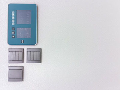
Overall, the digital cordless telephone with an answering machine is a favorite product. Also, it has an excellent star rating compared to other CD4012 phone devices.
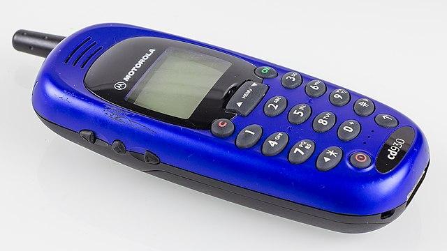
(An example of the Motorola CD series with a dialer type laser-etched backlit keypad).

How to use CD4012 IC?
First of all, the CD4012 IC needs a power source like every other circuit. Connect a power supply source to the IC via the Vcc/Vdd pin and the ground terminal.
By default, the operating voltage to apply is +5V. Nonetheless, an operating voltage range between +5V and +15V is okay.
On the other end, there is PIN Y for the output voltage. Often, this output voltage is equal to the CD4012 operating voltage. When one or both inputs are high, the output is high. This condition is proper when you observe the truth table of the NAND logic gate.
https://www.youtube.com/watch?v=NzGmgFRa_aQ
(Above is an attached video link for better understanding).
Applications Of CD4012
There are several applications in which CD4012 is important. To mention a few, they include
- Simple Logic Circuits.
- Logic Buffer circuit.
- Decoders and encoders.
- Oscillator circuits.
- De-multiplexers and Multiplexers.
- Networking systems.
- Lastly, in General, Digital Systems.
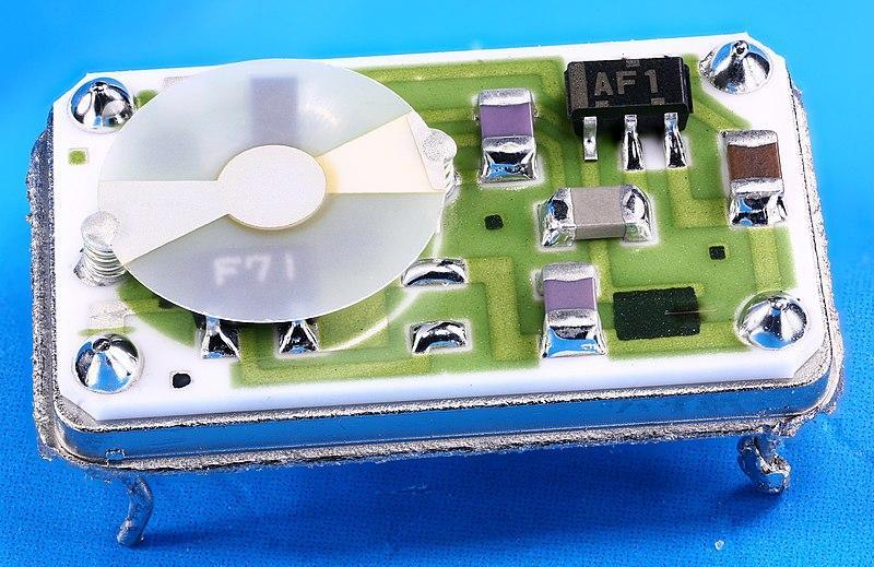
(An application of the CD 4012 IC in this crystal oscillator pictured above)
Conclusion
In a nutshell, the CD 4012 IC is a dual 4-in NAND gate made from CMOS technology. In addition, the NAND gate combines to form other logic gates like the OR gate, AND gate, and NOT gate. It is, therefore, famous for its use in logic inverter circuits, oscillator circuits, digital communication devices, etc. Another fine example is the Motorola CD4 series, with its large recording capacity and primary liquid crystal display.
So if you love to build circuits like the ones above, gain direct access to all the resources and guidance you need. Contact us today to get started.