Today’s technology is pretty different from what we had in the past. Interestingly, the size of electrical components is getting significantly smaller. And the same goes for printed circuit boards. Size reduction now allows PCB manufacturers to develop microcircuit boards. These micro designs are about half the size of the standard PCB. However, smaller boards require new design rules. So, this article will teach you how to build a micro-circuit board. You’ll also learn the micro PCB design guidelines and what you can do with these circuits.
Contents
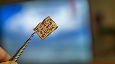
What is a Microcircuit Board?
Microcircuits are like regular PCBs but with smaller designs. These boards have more minor traces and vias, making designing smaller circuits possible.
A microcircuit board has different design methods compared to standard PCB design methods. It’s also more advanced—since you can’t use traditional materials and processes to make them. The way that works for designing microcircuit boards is Photolithography.
Interestingly, traditional PCBs have a minimum line width of 75 microns, while microcircuit boards can go as low as 30.
How to Make a Microcircuit Board
It would help if you first considered how small you want your fine lines. If you’re working with 30 microns, you won’t need the regular one-ounce copper layer. The more you reduce your line width, the more your thickness reduces.
However, thinner copper traces can’t pose problems to your circuit board. But, there will be problems if you’re working with high current applications. Thankfully, an easy fix would be using broader and specific traces to handle the high current flow.
Although fine lines of 30 microns are rugged and reliable, physical abuse can cause them damage. You can use solder masks to make them more durable to physical force.
Also, adhering copper to your circuit board’s surface can be tricky. However, you can use methods to adhere your micro traces to your board’s surface.
Moreover, you’d have to watch the physical limit for your small vias. If you’re designing below 50 or 2 microns, plating your board’s hole walls may not be easy, and you may create poor-quality vias.
Your laminate’s thickness also determines the minimum diameter of your Via.
Also, choosing new technologies over traditional circuit board technology would save time, effort, and cost.
Tips and Tricks to Create the Smallest PCB
- There are many things to note when designing microcircuit boards. These factors include minimum trace width, drilling hole, minimum solder mask clearance, text size, and many others. In truth, combining these factors will help determine your circuit board’s length.
- Another tip for creating small PCBs is always to consider your blind and buried vias (bed of nails). In addition, these factors are essential to your board’s design and help make it the smallest board possible.
- The vias’ role is connecting traces within the board layers. Also, more traditional options can reduce your board’s design routing space. But, you’ll need to find alternatives if you don’t want a large board. Blind vias can connect external and internal layers while reducing routing space. On the other hand, buried vias connect various inner layers, not external ones. Hence, you won’t need ample board space, and you’ll have a stable product.
- Also, don’t overlook the spacing between your components. If your design keeps your electronic components close together, it’ll eat up your trace routing space.
- Plus, a component with more pins would need more space. Hence, the proper spacing will make it easier to solder your parts on the microcircuit board.
- Lastly, always use the standard pin numbering for your board. That way, you’ll have fewer manufacturing concerns while reducing the size of your circuit board. It’ll keep things oriented and reduce risks during inspection and soldering.

Applications of Microcircuit Board
The need for small PCBs continues to grow as technology miniaturizes. Now, microcircuit boards can work with different applications. Some of these applications include:
- LED
- Semiconductor
- Microwave
- Industrial
- Instrumentation
- Power Electronics
- Contract manufacturing
- Medical equipment
Micro PCB Design Guidelines
Here’s a guideline to help you design micro PCBs.
1. Hole Sizes
When designing micro PCBs, you need to weed out every element of traditional PCB designs. Hence, you’ll need to run complete remodeling for your application to fit into a smaller size.
However, this task can be pretty challenging if you’re only well-versed in the ways of traditional designs. In truth, one mistake you need to avoid is creating large holes.
No doubt, your micro PCB won’t be as effective if the holes are too big. Instead, you’ll only produce a substandard or non-functioning micro PCB. Hence, it’s essential you only work with the proper manufacturer.
Manufacturers can serve as experts that help manufacture a micro PCB design—up to your standards.
2. Micro vias
You’ll need an HDI multilayer designing PCBs because of the HDI technology. So, copper layers can work as an HDI multilayer.
But that’s not all. You’ll also need micro vias because they can connect these thin copper layers.
Laser drills can help create holes with 2 to 3 mils thick diameter. Alternatively, you can make 5.9 mils through holes with 60 mils thickness.
But note that drilled holes aren’t the same as laser-drilled holes. While drilled hols have 12 mil pads with six mil holes, laser-drilled micro via have five mil pads and can use three mil vias.
3. Copper Thickness
Interestingly, one oz of copper is the standard thickness for a three-mil delicate line circuitry. Contrarily, microcircuits work with oz per 30 microns width.
For this reason, your traces don’t need to leave the board surface plating. All you need for manufacturing is regular pattern plating.
Also, pattern plating can make connections through your whole circuit. In contrast, wire bonding plating is electrical.
4. Electrical Testing
As technology evolves, we’ll need smaller landing pads. Right now, the lower limit of rigid or flying probe technology is 2-3 mil. However, it should get softer over time to fit with smaller circuit boards.
But, if you’re using more minor points on your micro PCB, like edge strip connectors, you should use extensions. In addition, you can use these extensional 3-4 mil pads to push your lines out of your circuit.
5. Identification Marking
Indeed, you can’t use the regular silkscreen images on your microcircuit. The reason is simple! It’s simply too big for smaller circuits.
Instead, you can try a more miniature identification marking resolution, like the inkjet printer.
6. Reliability
While you can use standard PCB laminates for microcircuits and HDI, there’ll be limits to what you can do with them.
Contrarily, you can use FR4-type laminates to manufacture single and double-sided microcircuits. But, these laminates must be thin enough for you to drill micro through holes.
7. Security Marking
Identification is not the only necessary marking needed. It would help if you also had security markings. In addition, it’s possible to insert your image into your solder mask. Hence, we recommend using bar codes.
These bar codes are way too small for human eyes to see.
8. Solder Mask
Recent technology allows us to create 30 micron fine lines. However, such technology is not present in solder masking.
The limit for solder masking is still 75-micron position accuracy and image resolution. Also, remember to use a lead-free solder alloy.
9. Final Finish
While you can use finishes for regular PCBs, we recommend using finishes specifically for microcircuits.
You can use wire bondable soft gold, silver, or immersion tin to finish your microcircuit design.
10. Check if Your Manufacturer is Capable

PCB Manufacturer
It doesn’t matter if you’re working with a specific application; it’s always important to know what your manufacturer can do. It’s a pretty important step in the micro PCB design process.
Things won’t be smooth if you work with a manufacturer that can’t meet your standards and specifications. Microcircuits are still complex, and some manufacturers may offer little or no help/support. Hence, before starting your PCB design process, ensure your manufacturer is up to par.
Also, note that your design must be within their guidelines. So, you’ll have to rework your plan if your manufacturer can’t meet your demands.
Reworking also causes delays and slows down the speed of the market and turnaround time.
12. Check-in with an Engineer
Once you’re sure your PCB manufacturing company can handle your base requirements, you should contact an engineer from that company. Ideally, it would help if you connected with this engineer throughout the design process.
The engineer would also serve as a guide for your micro PCB design. Unfortunately, many companies don’t offer engineer-led services.
So, if you can’t access support from an engineer, you should check out other manufacturing companies before you go deep into the design process.
Final Words
The advancements in technology demand much smaller circuit boards. Although these circuit boards are half or a quarter of regular PCBs, they don’t slack in terms of power and capabilities.
Additionally, these small PCBs have various applications and can create several products. They also make circuit designs more convenient than standard PCBs.
Also, remember that your circuit board’s size depends on your design. You can use design software to create layouts and quickly reduce the size of your circuit boards.
What do you think about microcircuit boards? Feel free to contact us if you want to manufacture your micro PCB.