Custom Circuit Board
- How do you choose a PCB that perfectly meets your specific needs?
- This friendly guide has all you need to know everything about a custom circuit board
- Where you can get the best custom circuit boards for your needs.
- We have professional standard reviewers that ensure strict quality control measures in every production process.
- We leverage advanced testing technologies, such as AOI Test, E-Test, X-RAY, and Impedance Control.
- We have an in-house PCB design and assembly process review, which ensures high-quality control. We are committed to helping you get the highest quality products and services at competitive prices.
- We use a wide range of PCB material options, such as FR4, High TG FR4, Rogers PCB, Metal-based PCB, and High-frequency Materials.
- We have a superior customer care department, which supports person-to-person services. Our customer care department is flexible and approachable if you want to make any updates before the production process begins.
PCB Manufacturing
Capabilities
WellPCB is a reputable and professional PCB manufacturing and assembling company with roots in China. The table below shows some of the primary capacities that we provide and support. It contains information about the PCB materials we use, the PCB technologies we leverage, the types of products we manufacture, and the tolerances we offer.
-
Materials:FR4, High TG FR4, Halogen Free Material, CEM-3, Rogers HF Material
-
Min.Contour Tolerance:+ / -0.1mm
-
Layer Counts:2-36 Layers
-
Min.Finished Diameter of PTH Hole:+ / -0.1mm
-
Finished Copper Thichness:0.5-5 OZ
-
Max.Board Thickness/Hole Ratio:12:1
-
Finished Board Thickness:0.2-6.0mm
-
Min.Solder Mask Bridge:4mil (Min,SMT Pad Space 8mil)
-
Min.Line/Track Width:3mil
-
Min.Legend(Silkscreen) Track Width:5mil
-
MIN.Drilling Slot Size:0.6mm
-
Surface Treatment:Leaded HASL, Lead Free HASL, Immersion Gold, OSP, Immersion tin, Immersion Silver, etc.
-
Solder Mask Color:Green, Black, Blue, White, Yellow, and Matt, etc.
-
Other Technology:Gold Finger,Peelable Mask, Non-across Blindried Vias, Characteristic Impedance Control, Riged-flex Board etc.
-
Solder Mask Hardness:6H
-
Legend/Silkscreen Color:Black, White, Yellow, and others.
-
Wrap and Twist:≤0.7%
-
Flammability:94v-0
The PCB Manufacturing
Process
We use the data (Gerber file) that you send us to create the production information for your customized boards. Our experts match your specifications with the capacities for compliance purposes.
When we make the circuit board, the imaging process is what defines the circuit traces. The traditional imaging process needs a UV-light and photo tool to transfer images. At the same time, LDI only uses a computer-controlled, highly focused laser beam to define the circuit pattern onto the board directly.
Here, we leverage the etching process to eliminate any undesirable copper residues from the panel. After removing it, we remove the dry film to remain with a copper circuitry, which is in line with the PCB design. So basically, etching is the removal of undesired chemical and electronic residues.
Lorem ipsum dolor sit amet, consectetur adipiscing elit. Ut elit tellus, luctus nec ullamcorper mattis, pulvinar dapibus leo.
We apply an oxide layer to the inner board layers and then stack them together using prepreg to create insulation between them. Additionally, we should add copper foil to the upper and lower stack parts.
In this step, we bore the holes that will later act as electrical contacts in the multilayer board. Drilling is a mechanical process that PCB manufacturers optimize to obtain registration to the internal layer links. It is important to note that we can still do laser drilling. We have a laser drilling machine, which can drill 3-6mil vias.
First, we apply some thin copper layer deposits on the holes we drilled earlier on the walls. PTH offers the best copper deposits, which conceal the hole walls and the whole panel. And this is a chemical process that we should strictly regulate to plate sufficient copper deposits into the non-metallic walls. Secondly, carry out panel plating to get a thicker outer copper deposit.
Outer layer imaging resembles the internal layering process. However, in outer layer drilling, we get rid of the dry film and maintain the circuitry. Then plate the extra copper later in a clean environment.
This is the second electrolytic plating process, where we carry out extra plating in dry film parts (circuitry). After depositing the copper, we should apply tin to prevent the plated copper from oxidation.
First, we take out the dry blue film. Secondly, we scrape all the unwanted copper residues. The tin deposits resist the etching process, therefore, protecting the copper deposit we want. Lastly, we chemically eliminated the tin residues to leave behind the circuitry.
With the help of artwork and Ultraviolet light, expose some PCB parts and remove all the exposed parts. Then completely cure the remaining solder mask to create a quality finish.
Surface finish can maintain the exposed copper circuitry meanwhile provide a solderable surface when soldering components to the PCB. Usually, metallic and organic are the two main kinds of surface finishes. Metallic surface finish includes HASL, ENIG/ENEPIG, Immersion Silver, Immersion Tin, while organic surface finish includes OSP and Carbon Printing.
We will test all the boards before shipping to ensure all of the printed circuit boards are free of defects and meet the standards you expect. Currently, we have two different types of testing equipment available to test the circuit boards. Some test machines include a flying probe, fixtureless testers. And we also have universal grid testing capability. These machines use fixtures built specifically for your PCB. If you have impedance control requirements, we will also test the impedance value of the coupon.
Here, we route the PCB production panels into particular sizes and shapes according to the production file. PCB V-Scoring is a process of cutting a ‘V’ shaped groove at the top and bottom of a printed circuit board, leaving a thin layer between the Vees. Once we have done this, it can easily separate the PCB Board at the V by applying minimal pressure.
In this step, a team of sharp-eyed individuals scrutinizes each product. The process involves visually examining the board in line with the set standards.
We pack your products by neatly wrapping them in materials that meet international packaging standards. Then we ship them through your preferred transport mode, mainly by DHL, FedEx, UPS, etc.
- Prototype orders placed within 24 hours
- Normal lead time (5-7 Wokring days for some PCBs prototypes and small batch production)
- Faster lead time (48 hours for some PCBs prototypes and small batch production)
why us
Since 2007, WellPCB has offered good-quality PCBs with excellent turnaround time and customer satisfaction. We are one of the biggest and most skilled board manufacturers in China. Our committed staff- with a rich experience in the electronic world- produce superior products, such as double-sided, single-sided, multilayer, and HDI PCBs.
Quickturn PCB Assembly
- PCB fabrication and parts procurement are carried out simultaneously, saving time
- Prototype orders placed within 24 hours
- Quote and Order Online at any time
Competitive Price
- Our price is one of the most competitive in the world
- Own factory with reasonable cost control, no hidden cost in it
- Accept T/T, cash, credit card, PayPal, bank transfer, etc.
- Our two factories have price support for different orders.
On-Time Delivery
- Standard methods are DHL and FedEx, door-to-door service. Average Shipping Time only 2-4 Days.
- Cooperate with two transportation companies for many years with discounted prices
- Anti-static+Moisture-Proof+Anti-Vibration Packaging; Inspection certificate
- Professional agent To Iran, Pakistan
Quality Assurance
- All products follow the IPC or UL Standards and the ROHS&REACH standards.
- 98% customer positive evaluation and satisfaction Standardized factory processes and management Multiple testing services
Return and Refund
- In case our PCB is not usable due to our fault, you can ask for compensation.
- We can refund your account directly or rework the unusable boards or re-fabricate your PCB and re-ship to you at our cost, but please cooperate to solve the problem if you need to rework.
PCB Factory Scale
We handle all production scales, including small, medium, and mass production orders.
Besides, we can deliver more than 10,000 products monthly.
We have competitive prices and unbeatable offers for volumes ranging from as small as 1 square meter for you.
Our Certifications
Here are the certificates we have:
IATF 16949:2016
ISO 9001:2015
ISO14001:2015
ISO13485:2016
UL
Also, all our products follow the IPC & ROHS Standards.
More importantly, we always strive to manufacture high-end PCB products.


PCB Product Show


Testimonial

NXP France
Top Questions
1. What services do you offer?
We offer three primary PCB assembly services: PCB fabrication, consigned PCB assembly, and full turnkey services.
2. Is it possible to get stack-up drawings from you?
Yes, we are willing and ready to share some of our standard stack-up drawings with you, or even individual stack-up drawings that meet your specific requirements.
3. Do you offer any discounts?
Our two factories offer price support for various orders, especially for multilayer PCBs and mass production.
4. Can you view and process Altium CAD data directly?
Unfortunately no. We generally deal with Gerber files.
5. What if I am dissatisfied with PCBs from WELLPCB.com?
If you encounter any problem with our products or feel dissatisfied with our products or services, you can let us know through [email protected]. We promise to get back to you within 24 hours and serve you satisfactorily. We will either refabricate your PCB in case of a defect or refund the full amount without needing to return the defective PCBs. You may also choose to credit your[email protected] account and use the credit for future orders.
Custom Circuit Board: The Ultimate Guide to How to Design
Every day, people depend heavily on electronic devices to get things done around the house and at their job places. These devices help us cook, clean, and do a host of other activities that would have been difficult or impossible to accomplish without them.
At the heart of every electronic is a printed circuit board (PCB). A PCB is a board that connects various electronic components in a particular device. So how do you choose a PCB that perfectly meets your specific needs?
This friendly guide has all you need to know everything about a custom circuit board, and where you can get the best custom circuit boards for your needs.
Table of Contents
Every day, people depend heavily on electronic devices to get things done around the house and at their job places. These devices help us cook, clean, and do a host of other activities that would have been difficult or impossible to accomplish without them.
At the heart of every electronic is a printed circuit board (PCB). A PCB is a board that connects various electronic components in a particular device. So how do you choose a PCB that perfectly meets your specific needs?
This friendly guide has all you need to know everything about a custom circuit board and where you can get the best custom circuit boards for your needs.
The Basics You Should Know About Custom Boards
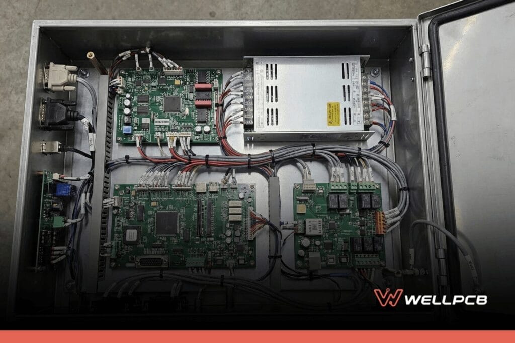
1.1: PCB Prototype Board
In the first phase of developing a custom board. It is much simpler to use a board designed for prototyping. Keep in mind that the fabrication and design of PCB will be required when it comes to adding the final touches to the end product.
1.2: PCB Material
Some of the materials needed for creating a custom circuit board include the copper clad board as well as the positive photoresist. The copper gathers on a foundation that’s referred to as the substrate. Designers can choose between one and two layers of copper, depending on what type of board is in use. There’s a silkscreen that helps make the PCB readable. The substrate, usually known as FR4 (Fire Retardant), works as a thick foundation for the PCB. On top of the copper foil is a layer that’s referred to as the solder mask. It’s usually green in colour.
Some PCBs do not use these materials. Instead, they use epoxies, which have the disadvantage of being thermally sensitive.
1.3: PCB Types
PCBs come in many types, depending on the intended use. The most prevalent custom circuit boards include:
1. Single-sided printed circuit boards
2. Double-sided PCBs
3. Multilayer PCBs
4. Rigid PCBs
5. Flex PCBs
1.4: Printed Circuit Board Components
All electronic components, regardless of their function, have individual components that are essential for various circuits. These components include LEDs, resistors, battery, transistor, switch, diode, and inductor.

How is the Custom Circuit Board Designed?
2.1: The Design Basics
Before we get started on the basics of custom Circuit Board design, we need to get familiar with some terminologies. These include:
2.1.1 Schematic Capture
It is a program that allows the operator to create a schematic diagram of the electronic component as well as other features. In other words, it’s a graphical representation of the element.
2.1.2 Gerber Files
These are computer-aided design files. The files are sent to the custom circuit board producers to assist them in building the PCB structure.

2.1.3 PCB Layout Tool
It is a program that allows for applying on multiple structures of the wiring connection structure. Once the construction is complete, the operator can then generate CAD files to be used to make the custom circuit board.
2.2: The Steps of PCB design
Different makers of printed circuit boards use different approaches when it comes to the designing of a custom circuit board. We’ve listed the essential steps below:
Step 1: Using of Software
Here, the designer chooses a suitable software to create a custom circuit board. One such software is EAGLE.
Step 2: Generating the Film
Using the finalized PCB diagram, the operator generates the film.
Step 3: Selecting Raw Materials
Where the intention is to design a simple device, the designer can use pocket-friendly material like paper phenolic that’s bonded with copper foil.
Step 4: The Drilling of Holes
Machines and drill bits help to drill holes at this stage. Both a hand machine and a CNC machine are applicable here.
Step 5: Fixing the Image
Here, the designer places a clean copper layer on the printer and stores the designed layout film on the computer before they print the command from the computer using a laser printer.
Step 6: Etching and Stripping
In this stage, the unwanted copper that’s attached to the custom circuit board is removed using different chemicals.
Step 7: Testing
It is the final stage, and it’s meant to ensure that the custom circuit board is fully functional.
Do You Know The Custom Circuit Board Software?
Currently, there’s a wide variety of software available in the market to help design custom circuit boards. Among the top software include: PCB Artist, Altium Designer 17, Ultiboard, DipTrace, SOLIDWORKS PCB, PCBWeb, BSch3V, Gerbv, XCircuit, Eagle PCBs, KiCad EDA, CircuitMaker, DesignSpark PCB, Pad2pad, ZenitPCB, OrCAD, CircuitStudio, PCB123, FreePCB and CUSPICE
3.1 Comparing Various PCB Design Programs
As you’ve seen, the list of software used for PCB design is long. We’ll pick two programs from the catalogue to compare. Of course, we can randomly select these two applications. Let’s take a look at DIPTrace and EAGLE CAD.
3.1.1 DipTrace
This software has many impressive capabilities. The program can perform schematic captures linked to the library. The software can also create patterns using a decent library editor. Users of this program can access tutorial and support. The software is also reasonably priced and has visually appealing colours. Generally, this software is ideal for small and simple custom circuit boards.
3.1.2 EAGLE CAD
This software is capable of electrical rule check, and forward and backward annotation between the PCB and schematic.
3.2. So what’s The Best Custom Circuit Board Design Software?
Given that there’s a great deal of circuit board design software in the market, putting your finger on the best among them is easier said than done. However, some design programs are highly recognizable due to their impressive functionality. One of them is EAGLE. This software is remarkably user-friendly and comes at a moderate price. The software can perform the batch execution of files as well as copper cladding.
Custom Circuit Board Layout Design
4.1: PCB Layout Design
The layout of a printed circuit board requires you to have some technical know-how and calls for the knowledge of software used to make PCB. You also need to be conversant with the computer-aided system used to make PCB, as well as have the skills required for the transfer of the basic PCB design to the final custom circuit board.
4.2: Comparing PCB Layout
When comparing various custom circuit board designs, we look at the following factors:
1. Board size
2. Layers available
3. Power delivery network
4. 3D modelling
5. Differential pair routing
4.3: PCB Layout Tutorial
Step 1: Converting the Schematic to a PCB
Once you have completed the schematics, click on “convert to PCB” on the specific editor you’re using. Doing so converts the schema to PCB.

Step 2: Dragging and Dropping the Component
Here, you place the document to the exact position you want it. If you prefer a neat looking custom circuit board, you can set the components that have a similar function next to each other.
Step 3: Sketch a Custom Outline
Here, you need to go to the layer menu and select the board outline layer. Then you click on the outline and delete it. Next, create your preferred shape using the printed circuit board tools.
Step 4: Copper Area
This step involves joining different parts to one signal. You can create a copper area with the tools menu.
Step 5: Routing
There are two ways to complete the route. Where there’s low current where you’re creating the custom circuit board, use the auto-router function at the top of the page to do it. Where there’s the need for different track sizes, it’s best to do routing manually.
Step 6: Holes
Irrespective of what you’re designing a custom circuit board for, you’ll still need to mount it on something. To create holes on the PCB for this function, use the Hole tool on the tools menu.
Step 7: Adding Pictures and Text
To add pictures and text onto the PCB, go to the tools menu, and stroll to find the text or picture tool. Position your preferred book or make changes as you wish.
Step 8: Photo View
As soon as you’re through with the above steps, it’s the time to view the result. In case you’re not happy with the colour or some other feature, you can change it. If you’re satisfied with the final result, click on “fabrication output.” That helps you buy the custom circuit board.
Printed Circuit Board Reverse Engineering
Sometimes, the schematic is not available. In such cases, you can produce replacement parts using the data created from the PCB reverse engineering. Reverse engineering a custom circuit board can be a tedious and challenging; process, but it still has to be done at times.
5.1 Why We Reverse Engineer PCBs
So why would we bother to reverse engineer circuit boards, given the time and effort involved? Well, here are just some of the principal reasons:
- To replace components on the PCB that have become obsolete
- Reposition some of the board components
- To improve the functionality of the circuit board
- Analyze and enhance security requirements
Conclusion
Given the enormous role that printed circuit boards play in electronic devices, the PCB you choose must be ideal for your needs. At the beginning of this article, we’ll tell you what’s involved in creating a custom board. I hope this information will help you. We also promised we’d help you find the right vendor for you. That’s where WellPCB comes in. When it comes to reliable, cost-effective, and durable products, you can count on us every time. Our PCB solutions are customized to fit your unique needs.
Would you like to discover more about our high-quality products? One call is all it takes! We have the best, and it’s all for just you.

Hommer
Hi, I am Hommer, the founder of WellPCB. So far we have more than 4,000 customers worldwide. Any questions you can feel free to contact me. Thanks in advance.