Contents
What is a loading line in BJT?
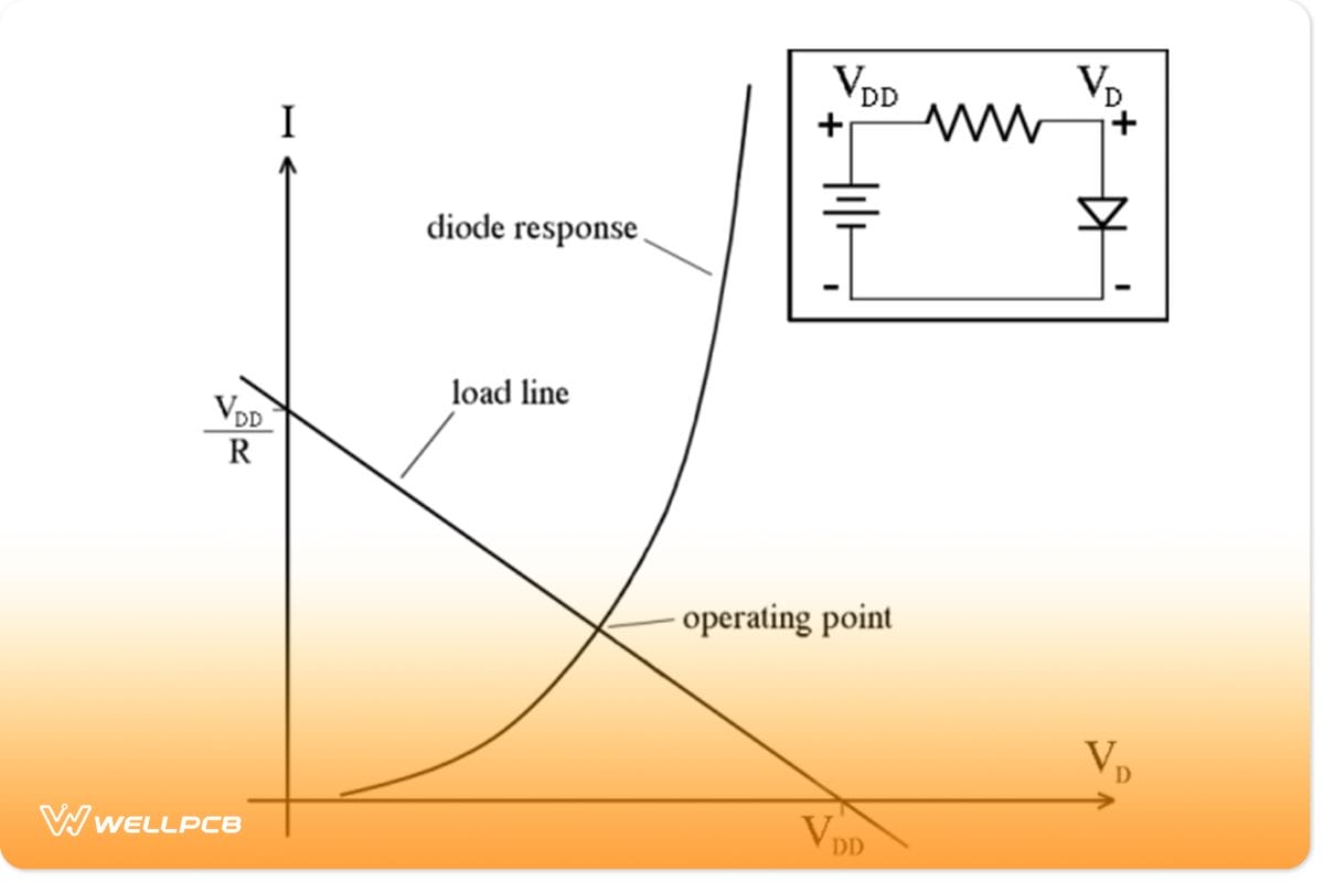
https://en.wikipedia.org/wiki/Load_line_(electronics)#/media/File:Load_line_diode.png
(Diode load line. The point of intersection gives the actual current and voltage.)
A loading line is a straight line that draws on the transistor output characteristics.
You represent a nonlinear electronic circuit graphically to determine its load line. As the line indicates, non-linear devices such as diodes or transistors can impose constraints on other parts of a circuit. The presence of a base current will turn on the collector-emitter junction. In turn, allowing a collector current to move through.
In the load line, you can see the relationship between current and voltage in the linear part of the circuit and the loop.
Transistor Load Line
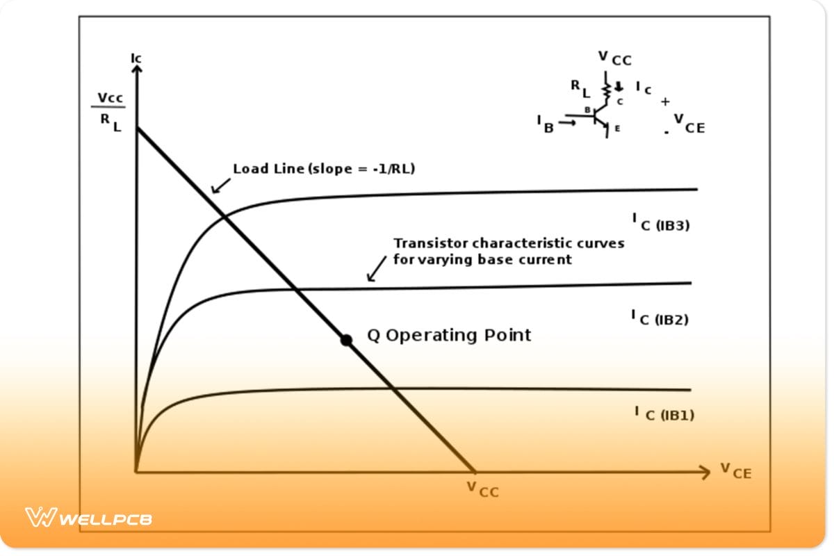
https://en.wikipedia.org/wiki/Load_line_(electronics)#/media/File:BJT_CE_load_line.svg
(A Load Line Diagram)
The load line diagram at the top is for a resistive load in a common-emitter circuit. It highlights how the collector load resistor, RL, restricts the circuit current and voltage. For each Value of Ibase, the transistor collector inductive current, IC, is plotted versus its collector voltage, VCE. Intersections of the load line and transistor characteristic curves represent circuit-constrained IC and VCE values at different base currents. It is important to note that the location of your load-line analysis and positioning is in the IC.
If the transistor could pass all currently available, with no voltage drop across it, the collector current would equal the supply voltage, VCC, over RL. It is at this point that the load line crosses the vertical axis. However, some voltage will always exist between the collector and the emitter, even at saturation.
The transistor current is a minimum of 0 when the load line crosses the horizontal axis. As a result, an entire supply voltage appears as VCE, with almost no leakage current passing through the transistor.
DC and AC Load Lines
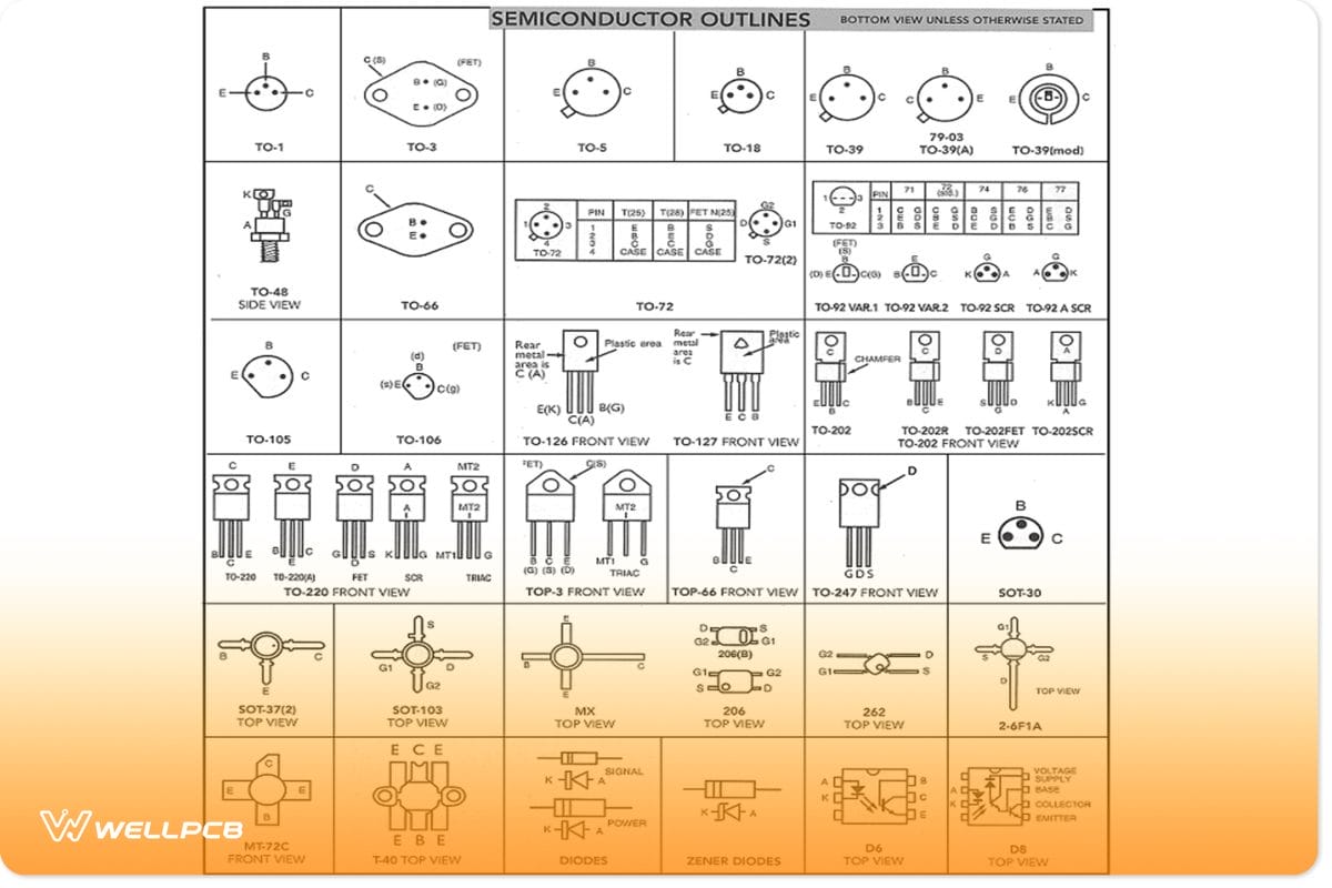
https://en.wikipedia.org/wiki/Semiconductor#/media/File:Semiconductor_outlines.jpg
(Semiconductor outline)
In semiconductor circuits, you add the input AC signal on the DC to bias the nonlinear semiconductor to the correct operating point, and the DC helps to bias the nonlinear semiconductor. It is possible to use separate load lines for the analysis of DC and AC.
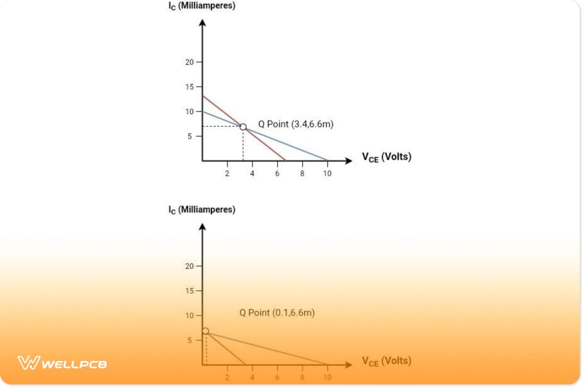
As you reduce the reactive components to zero, the DC load line is a DC equivalent circuit. It allows open circuits to replace capacitors and short circuits to replace inductors. A DC operating point, also known as a Q point, determines the correct DC point of operation.
By creating a current flow from the AC load line through the Q point, one can define the DC operating point. This line represents the AC load on the device, where the slope matches the AC impedance facing the device, which is generally different from the DC resistance.
You can determine the AC voltage to a current ratio of the device by this line.
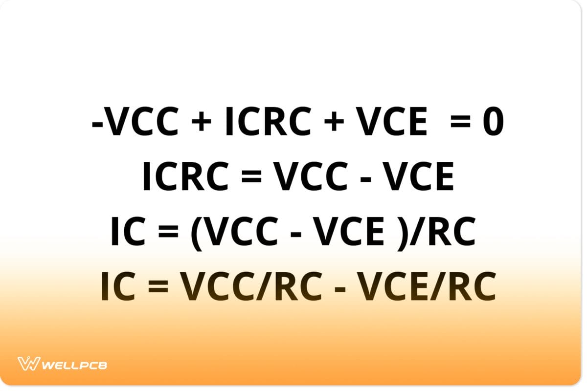
BJT load line Analysis Methods and q Point Analysis
(An equation of a load line)
Using the intersection of the load line and the device’s characteristics, one can determine the point of operation or the Q-point. You can call this type of analysis a load-line analysis. To find the Q point, you need to use Kirchhoff’s voltage law.
DC analysis
You will need to do a DC analysis to find the Q point. You exclude all AC voltage sources from a DC analysis since AC voltage sources are AC voltage sources. DC analysis focuses exclusively on DC sources. Due to their open nature, you remove all capacitors in DC circuits. You can find all the components before and after the capacitors, including the resistor, Rs, from the transistor circuit. This will help the diode remain in an active region. Remember that there is no input signal at the base terminal.
For a PCB project: PCB Layout Design allows a high-speed circuit board to function at its optimal but does require a vast understanding of signal integrity, power integrity fundamentals, and layout best practices. This will help you avoid the most costly design errors in your PCB board.
Maximum collector-emitter voltage and maximum collector current
To solve this part of the equation, you need to look at the collector-emitter voltage axis. If you look at the saturation region curve of collector curves, you will find the maximum collector-emitter current of the circuit. The curve intersection at the cut-off of the region of the collector curve will tell you the maximum collector-emitter voltage of the specific circuit for which you are doing the equation.
Finding the maximum symmetrical output voltage Swing
When you want to find the top symmetrical output voltage swing, you need to use the AC load line and determine how far the IC varies from the actual Q-point before the boundaries of the liner regions.
Taking the maximum output current swing and multiplying it by the resistive load resistance, the maximum possible symmetrical output voltage swing will be the maximum potential output current amplitude.
(Changes in Q points under different circuit parameters)
Final Thoughts
To summarize everything, A BJT load line is also known as Bipolar Junction Transistor. On the Y-axis, the collector current is at maximum. In other words, this is the saturation point. On the X-axis, the maximum collector-emitter voltage is shown when a figure is calculated for it.
You can optimize the performance of an active device if you know how to organize your equation correctly. You can visit our site to learn more.