Have you heard of Surface Mount Technology (SMT) and Through-Hole Technology (THT)?
They are two common ways to mount a PCB over another. However, this article presents a different type of technology: castellated PCB.
Castellations are pretty different from mounting technologies. They offer unique ways to solder two PCBs for one application. So perhaps the big question here is: What are castellated PCBs?
In this article, we’ll examine castellated PCBs in detail. We’ll also look at how to solder castellated edges.
Contents
What are Castellated PCBs?
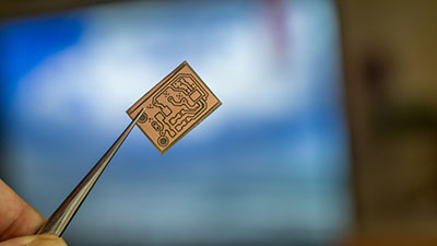
Castellations are crescent-shaped holes made at the edge of PCBs. Also, you can call these holes semi-plated holes. In addition, these holes make mounting PCBs easier and more convenient.
Castellations also help you align your boards correctly and make soldering easier.
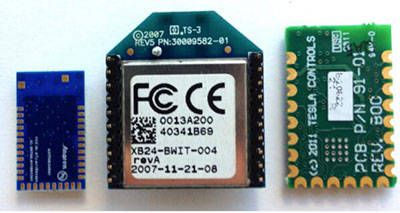
Furthermore, castellated PCBs use the board-to-board soldering mounting process. Plus, you can build different board modules with castellated holes. These modules can be wifi modules, Bluetooth modules, and many more.
Most importantly, castellations provide a direct connection between PCBs. So although you’re adding two boards to make one, the castellation system remains thin. In other words, the boards won’t become bulky after soldering.
Most designers prefer board-to-board soldering over other mounting technologies when mounting two PCBs is necessary. Also, castellated holes create links between modules and boards.
Why do We Use Castellated Holes?
There are several things we can do with castellated holes. First, most designers use them to create different PCB modules, including Bluetooth and wifi modules. Then, they can add these modules as independent units on a separate PCB during assembly.
Moreover, we use castellations when we need to combine two boards. We also use them for PCB links and wireless PCB to PCB connections.
Applications of Castellated Holes
There’s almost no limit to where you can use castellated PCBs. These boards can work in computers, power, telecommunication, high-end consumer electronics, industrial control, automobile applications, and more.

Computer Application
Advantages of Castellated PCBs
Castellated PCBs have several advantages. For example, we can create replicas of some parts of a PCB circuit with these holes. Picture this: if a course needs an inverter or feedback loops, you make dozens of these sub-circuits for testing.
That’s just an example of what you can do with castellated holes. Here are other advantages:
- You can use castellated holes to create wireless links between PCBs.
- Then, you can solder them to the main PCBs that need them. Also, it’s easy to mount castellated PCBs on another to make a final product.
- Additionally, castellated holes make changing pin layouts of components easy. Plus, you can switch your pins according to your requirements.
- Castellated PCBs can make small modules and breakout boards. These breakout boards can also work on certain parts of larger PCBs.
- Interestingly, you can use single PCBs to create integrated modules. Then, you can use these modules with other PCBs during production.

Plated Half Hole PCB Manufacturing Process
It’s pretty simple to manufacture conventional castellation holes. The usual process starts with drilling before applying chemical copper to the surface. Next comes panel plating and image transfer, then pattern plating.
Once that’s complete, the next is an etching, solder mask printing, and surface finishing. Lastly, we’ve hole castellation and outline milling.
Although the steps above are straightforward, they won’t give you the best results, especially in performance. However, there is a more advanced method of manufacturing plated half holes. Also, it’s pretty similar to the traditional approach, but there are slight differences.
The advanced method’s first step involves drilling your substrate plate edges. Plus, you must use only specialized drilling equipment for this task. Otherwise, there will be problems with the following step.
The next step is plating through the hole. Plating ensures your holes have a copper layer for better conductivity.
Recommended Specification for Castellated Holes
Castellated holes also have some design specifications you need to follow. These specifications include:
- Size: you can use the most significant size manageable
- Hole numbers: your design determines your number of holes. However, ensure your hole numbers are optimal. Or else, it’ll be half assembling and aligning your boards.
- Surface finish: your board’s application determines the type of surface finish. However, we recommend the ENIG surface finish.
- Pad design: we recommend using the giant pad possible on the top and bottom of your board.
Castellated PCB: How do You Solder Castellated Edges?
In truth, there’s nothing complicated about soldering castellated. You must ensure your board has to match castellated holes and footprints. Also, you need some soldering knowledge to avoid damaging your board.
If you’re new to soldering, you can learn more about the process here.
So, without further ado, here are the components you need for this project.
Castellated PCB: Tools Required and Specifications
- Soldering Iron: You can use any soldering iron with an adjustable temperature. Also, ensure it has a tip that can fit into the castellated vias of your board. Otherwise, you’d spill solder across your board and create solder bridges.
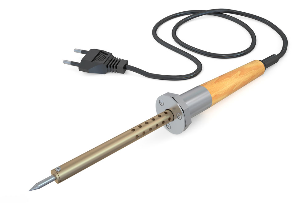
Soldering Iron
- Brass sponge: If you don’t have access to one, you can use a regular sponge with a bit of water.
- Solder: we recommend using a lead-free, water-soluble flux core solder, 0.020″ diameter solder.
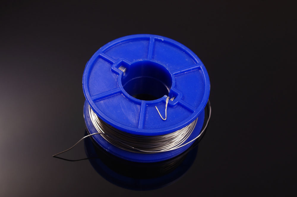
Solder
- Flux pen (water-soluble).
Source: Flickr
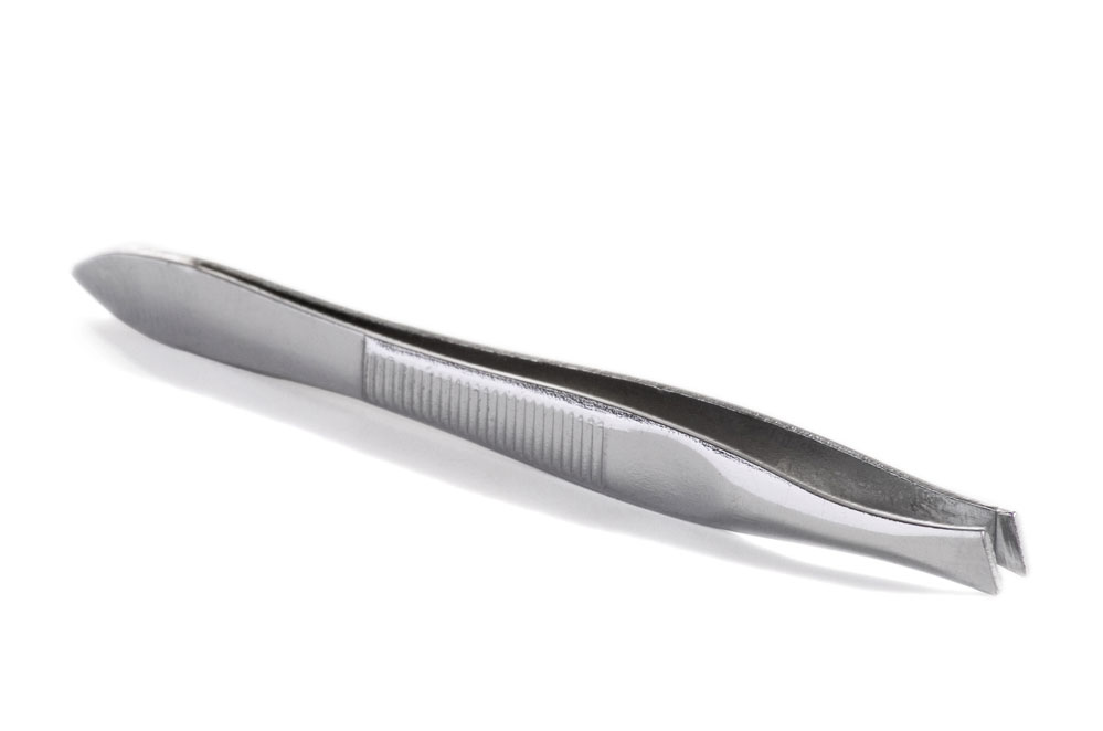
- Tweezers.
- Brush ( with ¼-inch bristles).
- Rubbing alcohol: you’ll need this to remove any flux left on your PCB to prevent damage. Usually, water-soluble flux needs hot and de-ionized water, but you can use rubbing alcohol instead.

Rubbing Alcohol
Optional Tools
- Tip tinner
- Solder wick
- Third hand or vice
- Low-lint wipes
- Diagonal cutters
Castellated PCB: Steps
Here are the steps you need to follow:
Step 1: Setting up a Work Station
Before you start, you’ll need a safe work area around your soldering iron. We recommend you:
- Keep your work area clutter-free and your tools nearby.
- Use ESD mats or other fire-proof surfaces so you don’t burn your table.
- Plug and turn on your soldering iron. Then adjust the temperature to about 370°C.
- If you have a regular sponge, keep it moist, not dripping wet.
Step 2: Clean Your Soldering Iron Tip
Here’s how to get this done.
You can apply some solder to the tip while it’s hot or put the tip into some tip tinner. The heat should melt the solder or tinner and form a coat.
Then, use your sponge to remove the extra solder or tinner. Also, repeat the process if your tip is not shiny and clean.
Step 3: Time to Solder!
Here’s where you need to be careful. So, we recommend starting with one corner pad on your pad. Then, gently hold the tip of your iron on the pad for about 1-2 seconds to start soldering.
Then, slowly put some solder between the iron tip and pad. Once the solder melts, you should have a nice mound of solder filling up the pad. Now, proceed to remove the remaining solder strand before the soldering iron.
Step 4: Add Some Flux
Time to add some flux to your nice mound of solder. However, be careful not to apply too much pressure, so the change doesn’t spill.
Step 5: Time to Mount Your Module
Grab your module and your soldering iron. Then, slide the module into place while keeping the mound heated. Also, ensure to use your tweezers to hold your module nearby while you melt the solder mount.
We want the castellation to take up some solder. So, it would help if you touched the via and pad with the melted solder. Also, adjust and align your module with the board while the solder is hot.
Note: Ensure your board faces the right direction so you don’t make soldering mistakes. Also, don’t touch the boards while the solder cools off.
Rinse and repeat the process for the other pins. Finally, inspect and ensure the solder touches the via and pad.
Final Words
Castellated PCBs are handy when you need to mount and wirelessly connect two PCBs. Interestingly, castellated holes make it easy to solder your boards together and even make adjustments to ensure they stay aligned.
Also, you must ensure the castellated holes and footprints (pads) match before mounting and connecting.
Do not hesitate to contact us if you want to build a castellated PCB.