About common PCB thickness, Regarding typical PCB thickness, It’s crucial to understand standards before setting the dimensions of your PCB. Although there’s no set PCB thickness standard, some specific sizes are shared among various manufacturing companies.
However, your projects may have different needs that require altering PCB thickness. So, how do you know what thickness is best for your PCB?
Read on to explore the factors that affect PCB thickness and what you should know before choosing one.
Contents
- 1 What is the Standard PCB Thickness?
- 2 Factors Affecting PCB Thickness
- 2.1 Copper Thickness
- 2.2 Board Materials
- 2.3 Size, Weight, and Flexibility
- 2.4 Signal Types
- 2.5 Vias Type
- 2.6 PCB Layers
- 2.7 Standard PCB Thickness: Operating Environment
- 2.8 Factors to Consider When Choosing PCB Thickness
- 2.9 Standard PCB Thickness: Equipment Capabilities
- 2.10 Standard PCB Thickness: Additional Cost
- 2.11 Standard PCB Thickness: Turnaround Time
- 3 Bottom Line
What is the Standard PCB Thickness?
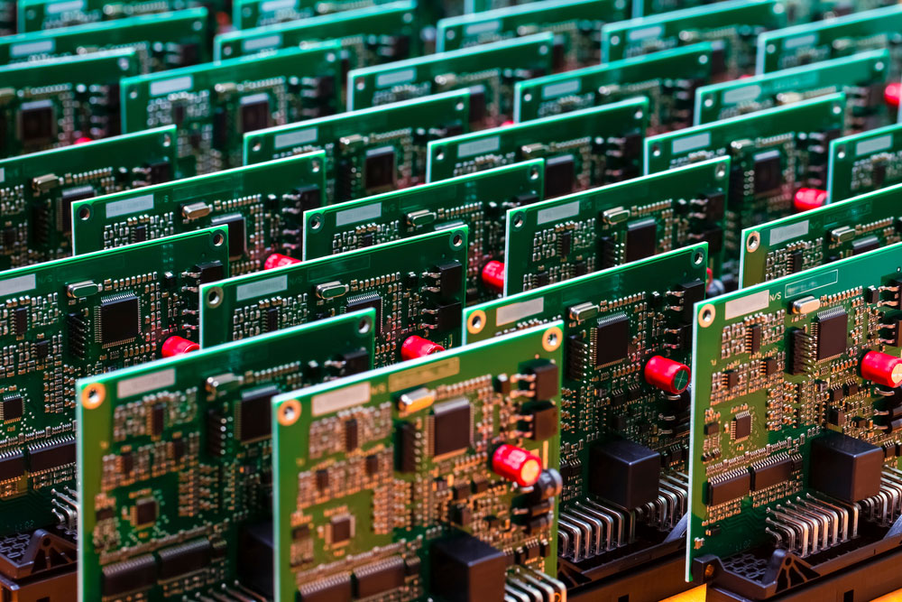
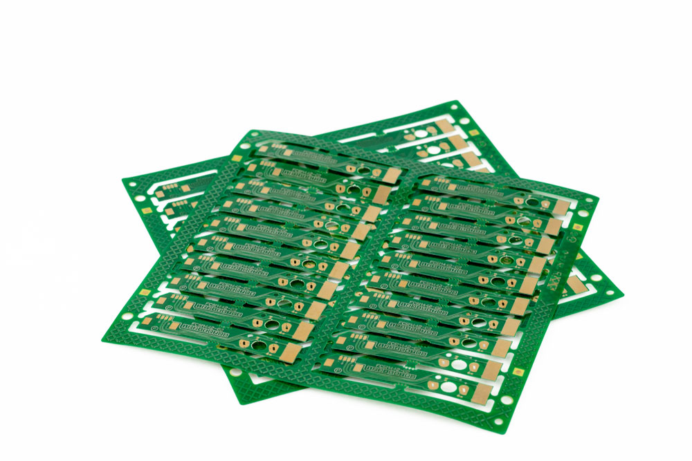
Rows of PCBs
As we mentioned earlier, there is no official PCB thickness standard. Moreover, the size popular among most manufacturers is 1.57mm (0.062 in.). There’s some truth in this, as this size was the standard PCB thickness for bakelite sheets during the earlier PCB fabrication era.
However, modern fabrication accepts various PCB thickness standards, including 0.78mm (0.031in), 1.57mm (0.062in), and 2.36mm (0.093in). So, it’s safe to say PCB thickness depends on your PCB assembly and fabrication choices.
Additionally, PCBs have various standards, including JIS, UL, IPC/JCA, and JPCA. These standards also help determine PCB thickness.

Factors Affecting PCB Thickness
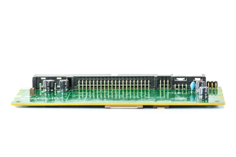
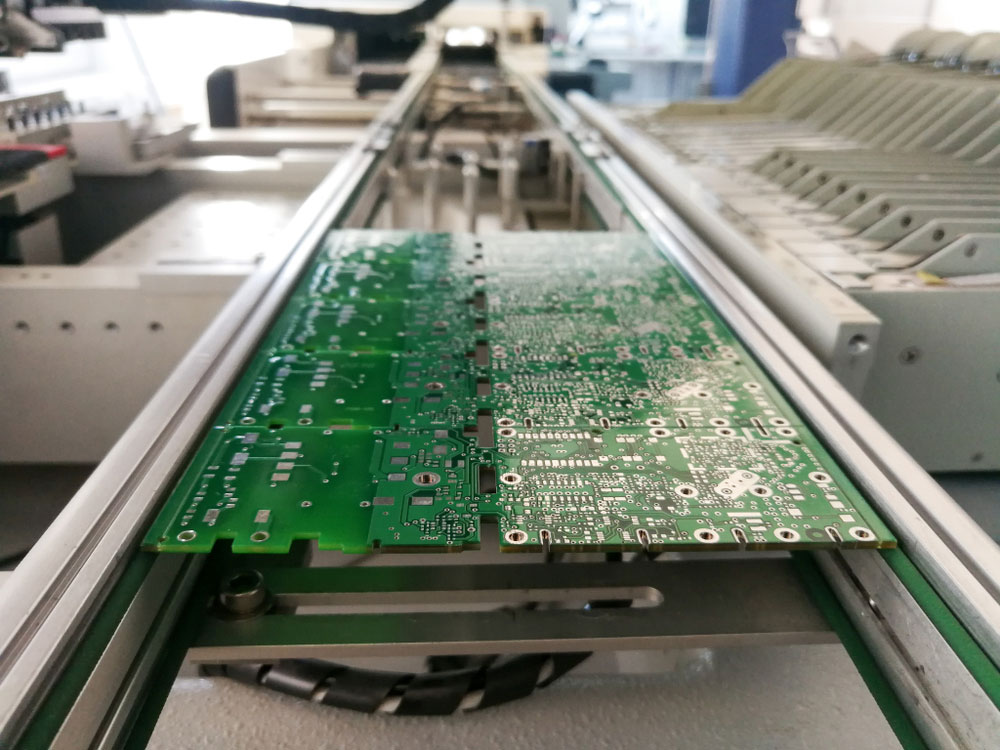
PCB Assembly
Several factors can affect your PCB’s thickness and force you to make adjustments. Sometimes, you may have to make custom requests to ensure your design has the right consistency. Let’s take a closer look at these factors.
Copper Thickness
Copper thickness refers to the diameter of your internal or external traces and pads. Generally, we can divide PCB thickness into three units: 1oz (35µm), 2oz (70µm), and 3oz(105µm). Moreover, the copper thickness depends on your board type.
2oz thickness works with high current traces used for switching power supplies. On the other hand, 1oz suffices for signal transfer and other regular operations.
Interestingly, 35µm takes up 70% of a PCB’s copper foil thickness. Factors influencing this include your PCB’s purpose, signal voltage, and current size.
Additionally, PCBs that require excessive current usually have 105µm and 70µm copper thickness on some of their traces and pads.
Furthermore, you can use 12µm for thin ultra-high density copper traces, like those on build-up boards. Also, 105µm always works for thick high-current trails as they are effective on boards that transmit large currents.
Board Materials
Slightly thick PCBs
The type of material you use for your PCB influences its thickness. And standard board fabrication requires substrates, laminates, silkscreens, and solder masks. Out of all these materials, the laminate and substrate are the essential ones to consider.
Why? Because they provide your board’s structure and influence its overall thickness. Usually, substrates consist of glass weave, epoxy resin, ceramic, or paper, depending on the required DK (dielectric constant).
Furthermore, laminates consist of cloth, paper, or thermoset resin layers. And all these materials offer options that determine your PCB’s overall electrical, thermal, mechanical, and thickness properties.
Size, Weight, and Flexibility
Flexible PCBs
Generally, applications affect your PCB thickness. So, you’ll have a lighter and more flexible consistency for thinner PCBs. But, your board may break easily. If your applications don’t need flexibility, slightly thicker boards will give you more structural integrity.
But, thicker boards tend to take up more space and are weightier than their thinner counterparts. And it may cause issues for lightweight devices and applications with limited space.
In short, your final application affects the thickness of your PCBs.
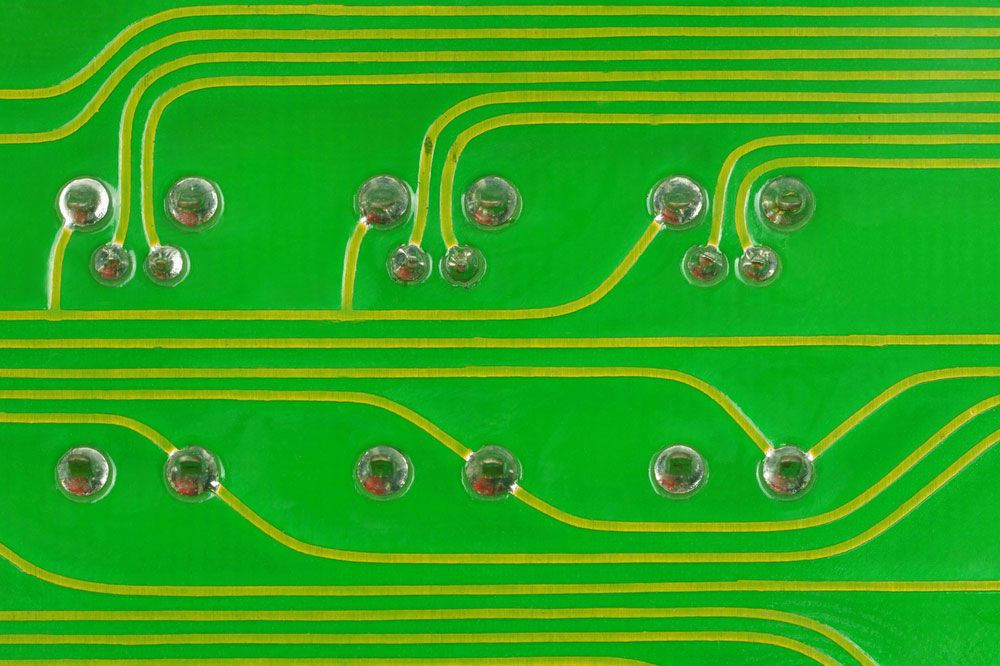
Signal Types
Signal Traces
You can use several signal types on your PCB. These signals determine your board’s materials and also influence the thickness. For instance, high-power PCBs are generally thicker than low-power versions.
Also, high-power PCBs need wider traces and thicker copper to handle the high-power signals.
Contrarily, high-density boards are usually thinner than other PCB types. Why? Because their complex signals use thin high-performance materials, traces, and laser micro vias.
Vias Type
PCB Vias
Visas are necessary for routing traces through a PCB. And it’s essential for building minimalistic designs.
Additionally, there are five types of Vias with different densities. And each variant has a set thickness value. So, for instance, you can use micro vias on thinner boards and through vias on slightly thicker boards.
The visa types include:
- Via-in-pad
- Through via
- Blind via
- Micro via
- Buried via
PCB Layers
Designs with multiple layers are usually thicker than those with fewer layers. Although it’s possible to stack thinner layers, it becomes impractical as the number increases.
PCBs with two to six layers may have standard thicknesses, while those with eight layers and above have greater thicknesses.
Standard PCB Thickness: Operating Environment
Your PCB’s thickness and materials influence its resistance and conductivity, making it necessary to have thicker PCBs in specific conditions. For example, thinner boards won’t work in rough operating environments, while wider boards may fail in thermal environments.
Factors to Consider When Choosing PCB Thickness
Some designers may opt for standard PCB thickness, while others may choose to customize. Although your application will help you choose, the final PCB thickness will determine your manufacturing costs.
Here are some factors you should consider before choosing PCB thickness.
Standard PCB Thickness: Equipment Capabilities
PCB in Equipment
First, you should ask if your manufacturer has the necessary equipment for your needed thickness. And ensure you partner with manufacturers that accommodate your requirements, especially if your design needs some advanced machinery.
Note: More advanced design techniques will attract higher costs.
Standard PCB Thickness: Additional Cost
Confirm if a custom board will be cost-effective for your project. For example, boards within the standard thickness threshold are more affordable than customized variants. On the other hand, thicker boards are more expensive and take time to manufacture.
Standard PCB Thickness: Turnaround Time
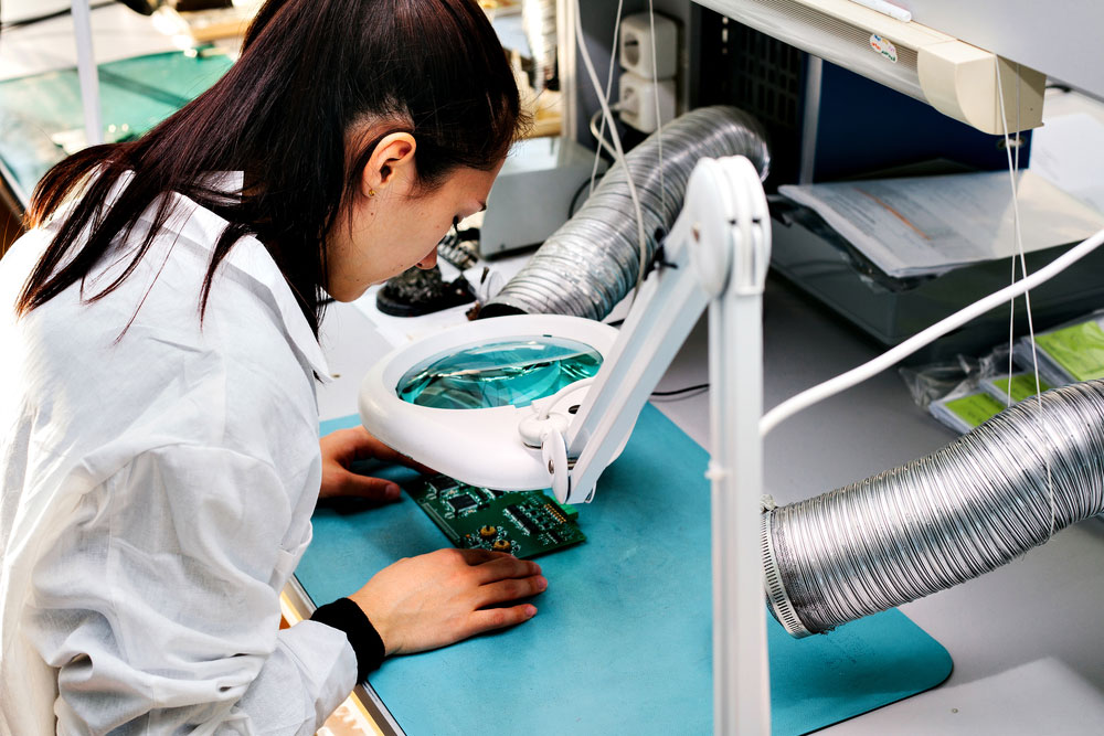
Careful PCB Assembly
PCBs with custom thickness requires more manufacturing time. In addition, they may require manufacturers to modify their processes and settings to meet the design’s unique requirements.
These adjustments are not quick and will cause delays. Thus, having proper schedules and delivery estimate discussions with your manufacturer is best to get a shorter turnaround time.
Bottom Line
PCB thickness is a crucial factor that determines your board’s effectiveness. And using the wrong thickness for your projects may cause damage or operation failures.
Although you can order custom PCB thicknesses, we recommend fitting your designs to the traditional values. In addition, custom orders may take a lot of time and money to manufacture.
Do you have more questions? Contact us, and we’ll be happy to help.