Contents
What Are High-Speed PCBs?
High-speed PCBs refer to circuit boards that facilitate or transmit high-speed digital signals. You can identify the speed of the digital signal by its rise or fall time. We mainly use the former (rise-time) because fall times are harder to measure.
Any signal with a rise-time of five nanoseconds and below is a high-speed signal. Likewise, any signal above this cutoff is a standard or low-speed digital signal.

a high-speed signal
Distinguishing high-speed PCB designs from standard ones isn’t always straightforward, and even seasoned electronic engineers can have trouble separating the two.
Both types can share similar components and layouts, making it difficult to recognize when a design crosses into high-speed territory.
Some may go as far as misapplying performance metrics like clock frequency.
When clock speeds increase, it introduces complex dynamics like signal integrity, crosstalk, and electromagnetic interference, which impact performance.
Failing to address these as part of the design factors can lead to system instability, signal degradation, or outright failure.
Ultimately, standard PCBs do not support high-speed digital signals, whereas high-speed PCBs do. Some common uses for high-speed PCBs include:
- Aerospace and military applications: High-frequency communication devices and systems.
- Medical devices and equipment: Advanced diagnostic tools like magnetic resonance imaging (MRI) machines.
- Industrial and manufacturing industry: Automated machinery and power amplifiers.
- Telecommunications: Nodes, satellite receivers, decoders and networking equipment.
- Consumer electronics: Personal computers, wi-fi routers, modems, graphics cards, etc.
Key Principles of High-Speed PCB Design

In addition to signal speed, there are other factors to consider when determining the quality of your high-speed PCB design—mainly signal integrity.
Signal integrity describes the potency or quality of the digital signal. The higher the signal speed (and frequency), the more susceptible it is to degradation.
In addition to the structure of the PCB, three main focus points relate to integrity:
- Electromagnetic Interference Compatibility (EMC): Refers to the (lack of) susceptibility the signal or device has to electromagnetic interference as well as the (lack of) interference it creates.
- Power distribution: How the PCB distributes power to its various components.
- Thermal management: Heat and cold affect the material properties of the PCB. These can affect signal integrity positively or negatively.
What Are the Challenges in High-Speed PCB Design?
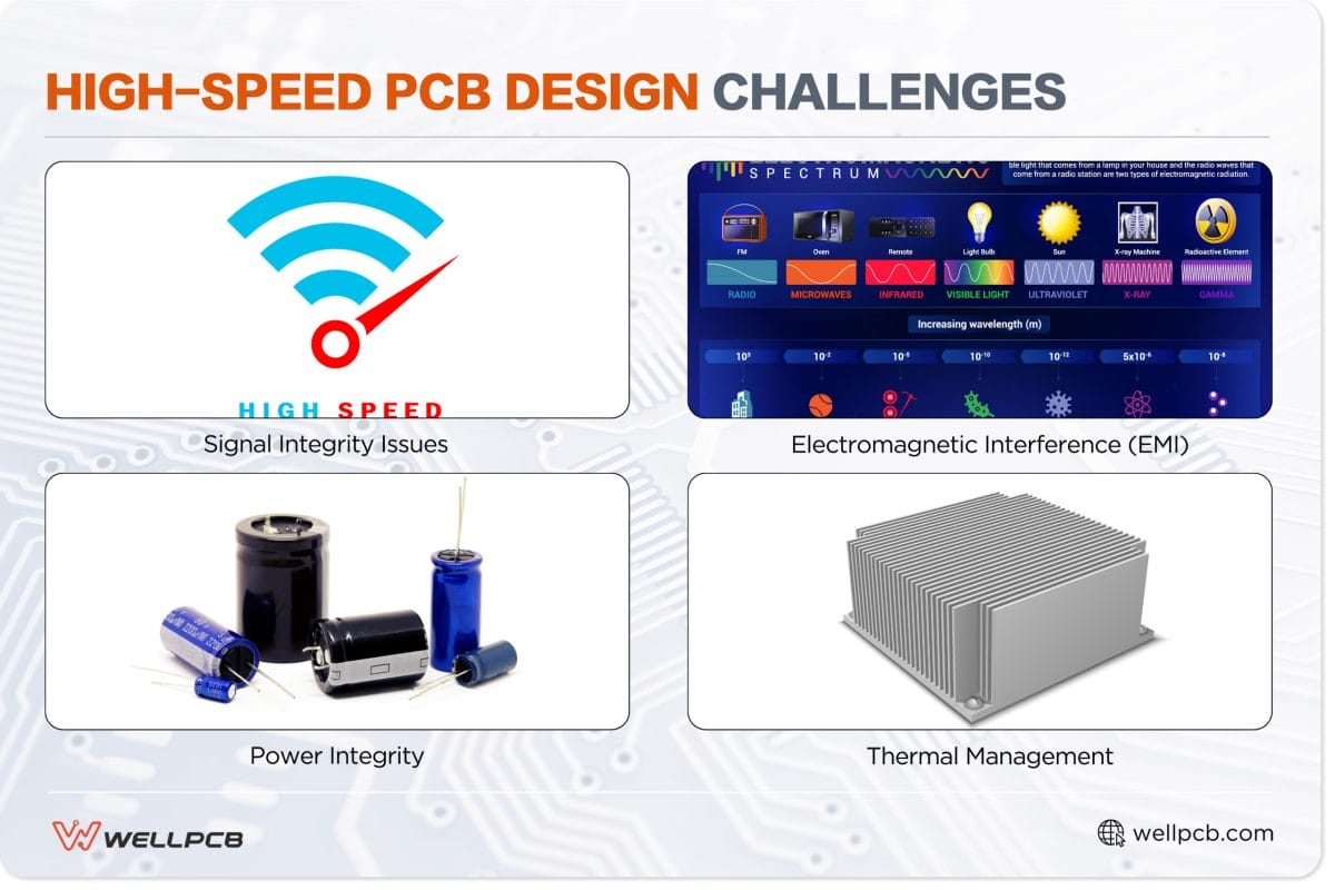
Challenges in High-Speed PCB Design
High-speed PCB design presents a unique set of challenges that can significantly impact performance and reliability. To address these challenges, you need a thorough understanding of various technical issues and how to apply specialized design strategies.
Signal Integrity Issues
The longer the medium that a signal has to travel across, the higher the risk of signal degradation.
In most instances, your PCB may have the necessary pathways to accommodate high-speed signals. However, because your design forces these signals to travel distances that diminish their integrity, your PCB may not perform like a high-speed PCB design.
You can typically address these issues by reconfiguring your design’s stackup, redoing its routing, and adding more terminations.
Nevertheless, these aren’t the only issues related to signal integrity that your high-speed PCB design may face.
As a signal speed increases, so does its frequency. This makes it more prone to unintentional electromagnetic coupling (cross-talk), simultaneous switching noise (ground-bounce), ringing and reflections, electromagnetic interference (EMI) and impedance mismatch.
All of these issues are related to signal integrity, and they can noticeably stifle the performance and dependability of your high-speed PCB design.
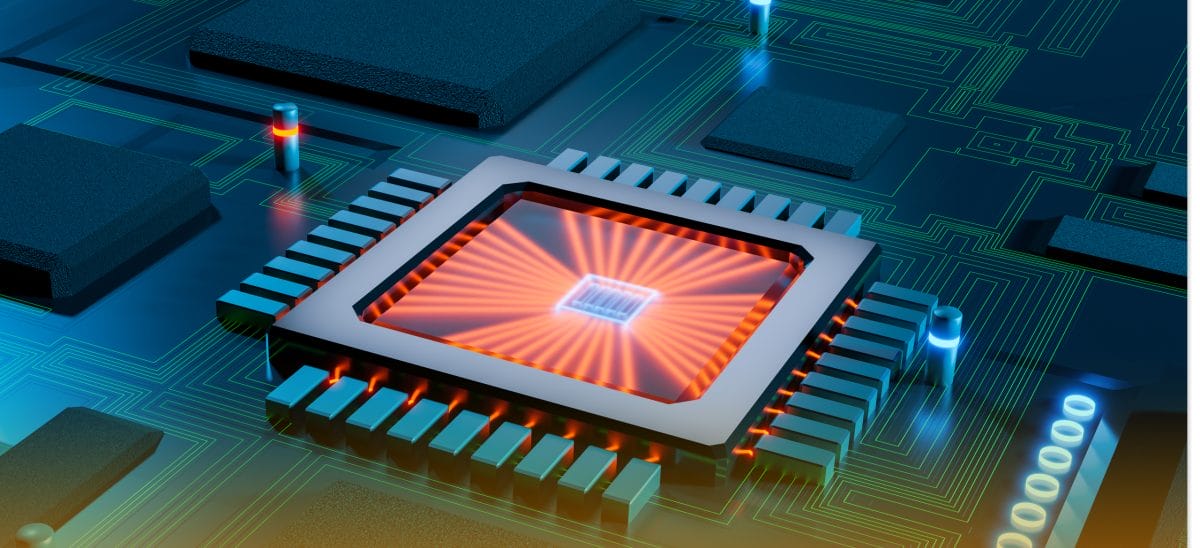
View CPU Processor Chip On Circuit
Electromagnetic Interference (EMI)
Any element with an electromagnetic field can interfere with digital signals. This applies to the current running through your PCB, too.
Electromagnetic interference may also come from a source outside of the system. Most modern electronic devices emit electromagnetic radiation, so your design must protect your PCB from internal and external electromagnetic interferences.
We use the principle of electromagnetic compatibility to address EMI.
By implementing ground planes, optimizing the trace layout, arranging components accordingly, and adding EMI shielding, we can significantly reduce signal degradation due to EMI.
Power Integrity
The power integrity of the PCB refers to how efficiently it distributes power. It primarily hinges on the PCB design’s power distribution network (PDN).
Suboptimal PDN design can lead to voltage droops and noise interference. These issues can lower the signal integrity of your PCB, as well as its general stability and performance.
Tackling power integrity-related signal degradation comes down to managing the placement and usage of PDN components.
These components include power sources, traces, PCB planes, decoupling and bypass capacitors, and voltage regulators.
Decoupling and bypassing capacitors can have the biggest positive impact on the power integrity of your PCB.
They allow the PCB to deal with sudden voltage fluctuations by storing and disbursing energy as needed.
When using capacitors to optimize your PCB’s PDN, consider the distance between capacitors and power pins, your capacitor values, and the distribution of capacitance.
Thermal Management
Another property to pay close attention to is your design’s thermal management capabilities. Heat, in particular, can massively disrupt your design’s signal integrity.
There are two main techniques that can help you maximize thermal management. These consist of adding new components to aid with heat dissipation and altering the placement of your PCB’s functional components.
You can use components such as heat sinks, thermal vias, and heat pipes to help deal with the heat generated by your PCB.
However, before you attach these components to your design, you must identify your PCB’s hot spots. These refer to areas that generate the most heat on your design.
Material selection and usage play a huge role in thermal management.
Pay attention to the substrate material and its density, trace copper weight and thickness, and the structure and layout of your pads.
All these factors will affect how well your PCB dissipates heat.
Another consideration is the placement of components.
High-power components such as oscillators, integrated circuits, and diodes tend to generate the most heat. Consequently, they should sit as close to the edge of your PCB as possible, allowing heat to escape more freely.
What Are the Best Practices for High-Speed PCB Design?
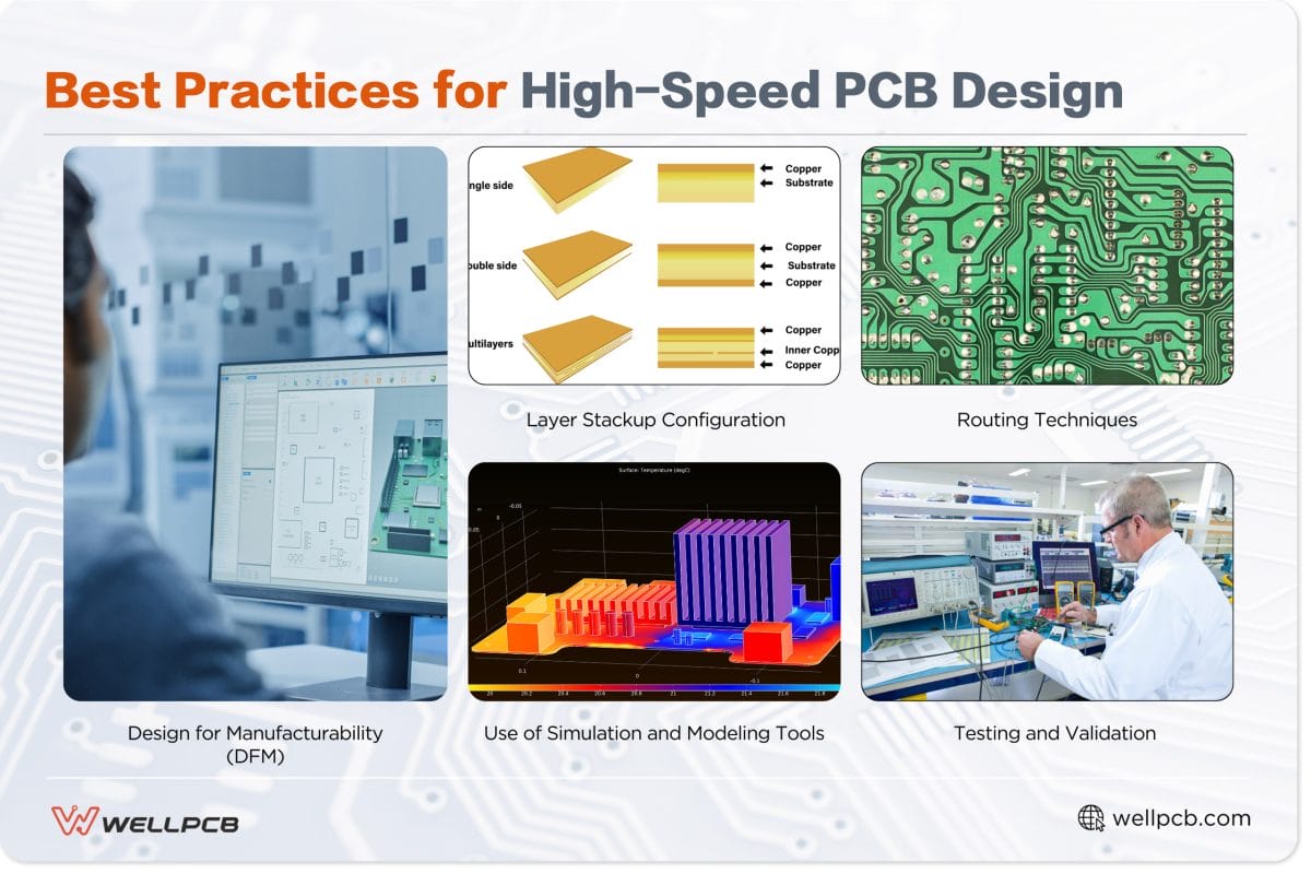
Best Practices for High-Speed PCB Design
Follow these best practices to ensure that your design not only meets the technical requirements but also aligns with manufacturing and testing standards.
Design for Manufacturability (DFM)
The fabrication of high-speed PCBs is substantially more complex than that of standard PCBs. High-speed designs seldom use single-layer boards. While it’s seemingly more challenging to design high-speed PCBs for manufacturability, it’s still a must.
By designing for manufacturability, you can ensure that your design meets the manufacturing standards of most PCB fabricators. It will also reduce incidents of manufacturing errors.
It’s best to consult the IPC-2141A when designing high-speed PCBs. This industry-issued standard acts as a design guide for High-Speed Controlled Impedance Circuit Boards and is recognized by most (reputable) manufacturers around the globe.
The IPC-2141A contains guidelines on material selection, approaches to fabrication, testing techniques and computer-aided-design (CAD) software process rules.
Layer Stackup Configuration
Improper signal return paths resulting from a suboptimal layer stackup are another common cause of signal integrity issues in high-speed PCBs.
However, that’s not the only thing to worry about when finalizing your stackup. Channel spacing, routing and EMI shielding are all crucial considerations.
Generally, it’s best to place signal return paths on adjacent internal reference planes. These reference planes should be clear and unbroken.
In addition, reference planes must limit inductance while ensuring the correct amount of impedance established by the design guidelines.
In most cases, high-speed PCB designs utilize a stripline or microstrip configuration.
Stripline configurations feature internal trace routing that sits between two reference planes, while microstrips consist of a surface trace stacked on top of a single reference plane.
The impedance and inductance requirements of your design, along with its trace properties, dictate which configuration you should use.
Routing Techniques
You should only conduct routing after you’ve arranged your components on the board. This will give you an idea of how you should approach the routing process.
Keep routing as direct and short as possible for high-speed signals. Remember, the longer the path that the digital signals have to travel, the greater the risk of signal integrity loss.
According to best practices, your design should minimize current loops and keep signal return paths as direct as possible.
One way to achieve these design requirements is through the usage of vias. While some sources recommend avoiding or limiting the usage of vias, if they’re critical in your design, try not to use standard surface vias.
Instead, use microvias and buried or blind vias. Return path vias can help you keep current loops short.
Avoid routing over ground plane breaks and voids at all costs. Failing to steer clear can result in impedance mismatches and EMI issues.
Also, keep away from running unidirectional high-speed transmission lines in parallel, as this can increase the risk of a cross-talk. Instead, route differential pairs as symmetrical opposites.
Use of Simulation and Modeling Tools
You can use thermal modeling software to simulate how well your design dissipates heat. Simulation and modeling tools are essential in high-speed PCB design as they allow you to test your design without fabricating a prototype.
The thermal management of your PCB is not the only element these tools reveal. They allow you to predict your design’s PDN performance and mitigate issues related to your stackup.
Since it’s crucial to maintain signal integrity in high-speed PCB design, your CAD software must allow you to test this specific property.
Look for simulation or CAD software that offers a crosstalk waveform calculator, as well as reflection and ringing detectors.
Testing and Validation
While simulation and modeling tools help mitigate errors, they cannot eliminate them entirely. As a result, prototype testing and validation are crucial in design and manufacturing processes.
They allow you to verify the real-world performance of your high-speed design.
While many often tout the importance of designing for manufacturing, they seldom speak about designing for testing (testability). This is because the space constraints of high-speed designs can make it more complex to add the necessary test points.
Nevertheless, when dealing with high-speed signals, you should implement elements such as test traces, LEDs, headers and other test components.
When paired with techniques like in-circuiting testing, these components allow you to verify the quality of your PCB.
However, if you want to test signal integrity specifically, use a vector network analyzer or eye diagram test.
How We Commit to High-Speed PCB Design Quality
At WellPCB, we leverage a combination of thorough design processes and proprietary technologies to meet and exceed industry expectations.
Our Design Processes
As we know, DFM is instrumental in ensuring the success of your high-speed PCB design. Therefore, WellPCB performs full design rule checks (DRC).
We accept Gerber, .pcb, .pcbdoc and .cam file formats. We’ll verify your design files to ensure they’re viable for fabrication.
We support the manufacturing of rigid PCBs with up to 32 layers. In addition, we also offer assembly services where we source all the components for your design.
You can trust us to deliver a high-quality PCB turnkey solution. We hold the following qualifications:
- ISO 9001:2008
- UL Certification
- ISO / TS 16949:2009
- ISO 14001:2004
Proprietary Techniques and Technologies
Integrating vias and performing optimal routing for your PCB layout can be difficult. Not all manufacturers can meet these fabrication and assembly demands.
We offer on-across blind vias and characteristic impedance control to help you maintain your designs’ signal integrity.
What are Industry Innovations and Trends in High-Speed PCB Design?
The PCB industry is rapidly evolving, driven by innovations that address the increasing demands for performance and reliability in electronics.
Understanding the direction of travel is essential for leveraging the latest technologies and techniques to enhance design efficiency and effectiveness.
Recent Technological Advancements
As we now know, balancing signal speed with signal integrity is largely the hardest part of designing high-speed PCBs. In response to this, the industry has been developing ways to make it easier for designers and manufacturers.
As we find and use new materials, we can limit crosstalk and EMI while enhancing signal integrity for high-speed data transmission.
Microvias allow us to fit more components on the PCB while enabling more precise high-speed routing.
Future Trends To Watch
It’s likely we’ll see an even greater emphasis on high-density interconnect (HDI) technology.
The layer density and surface space that this technology offers will allow designers to fit more components on more compact PCB form factors.
Although many encourage the usage of through-hole vias to reduce reflection, the refinement of Surface Mount Technology will continue. SMT packages and components offer better thermal management and are easier to assemble at speed.
Conclusion
Ultimately, limiting your assessment of high-speed PCB designs to the frequency and speed of its signals is never a good idea.
While these values are important, other factors, such as electromagnetic compatibility and power distribution, can negatively impact the board’s signal quality.
Even if all metrics and measurements point to your board being capable of accommodating high-speed signals, it may not be a true reflection of these capabilities in the real world.
Get Started With Our High-Speed PCB Design Services
So you’ve established and optimized your high-speed design, what’s next? Why not engage with a reputable manufacturing partner with over a decade of service experience?
Use our online quote generator to see how much you stand to save by using our services.
You can also fill out a contact form, and one of our friendly consultants will contact you as soon as possible with more information.