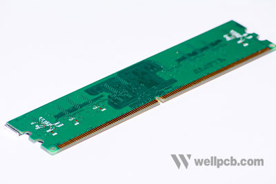
When ordering multilayer printed circuit boards, it is essential to ensure that you purchase them at reasonable costs. However, a majority of customers who need them only consider the aggregate price, including cost expenditures.
Helping customers in reducing the costs of their multilayer PCBs during the manufacturing process is a top priority for plenty of manufacturers. However, there are simple ways or means in which multilayer printed circuit board customers can learn regarding how to reduce their costs during a multilayer PCB manufacturing process. Here are 9 effective ways to reduce costs in multilayer correct PCB service provider. Thankfully, there are various PCB manufacturing.
Contents
- 1 Multilayer PCB Specification
- 2 Trace Width and the Spacing
- 3 Plating and Finishing
- 4 Mass Production
- 5 Limit the Number of Geometries
- 6 Adherence to Recommended Tolerance
- 7 Maintain Enough Spacing Between Copper Layers
- 8 Multilayer PCB Manufacturing– Drill Size
- 9 Multilayer PCB Manufacturing– PCB Material Selection
- 10 Summary
Multilayer PCB Specification
Trace width matters because the right trace width ensures that the trace, regardless of whether it’s for power or signal, operates as desired while providing the optimal function of a printed circuit board. Generally, though, trace widths carrying signs can be smaller than those used in carrying current.
Customers who get to order multilayer printed circuit boards can reduce related costs or purchase them cheaply by ensuring that the manufacturer reduces trace width and spacing. Unfortunately, though, most customers aren’t aware that issues to do with track width and spacing during the design stage can significantly affect the cost of their printed circuit boards. To ensure that you keep manufacturing costs low, you need to select dimensions that give you the room to finish your layout comfortably.
You need to be aware that the closer the spacing is, the higher the costs of manufacturing your printed circuit board’s design. While trace and width spacing comes in as essential features, especially on a multilayer printed circuit board, it is necessary to reduce trace and width spacing.

Trace Width and the Spacing
Trace width matters because the right trace width ensures that the trace, regardless of whether it’s for power or signal, operates as desired while providing the optimal function of a printed circuit board. Generally, though, trace widths carrying signs can be smaller than those used in carrying current.
Customers who get to order multilayer printed circuit boards can reduce related costs or purchase them cheaply by ensuring that the manufacturer reduces trace width and spacing. Unfortunately, though, most customers aren’t aware that issues to do with track width and spacing during the design stage can significantly affect the cost of their printed circuit boards. To ensure that you keep manufacturing costs low, you need to select dimensions that give you the room to finish your layout comfortably.
You need to be aware that the closer the spacing is, the higher the costs of manufacturing your printed circuit board’s design. While trace and width spacing comes in as essential features, especially on a multilayer printed circuit board, it is necessary to reduce trace and width spacing.

Plating and Finishing
Another factor to consider when it comes to multilayer printed circuit boards is the cost associated with plating and finishing. Some finishes bring about high-grade multilayer printed circuit boards with longer shelf life, thereby increasing manufacturing costs. One of the most favorable and highly low-cost finishes is HASL.
When you want to reduce the costs of producing your multilayer printed circuit boards, ensure that you go for cheaper plating and finishing procedures. Not all of them are low-cost. For instance, a finishing procedure such as Electroless Nickel Immersion Gold is expensive, especially if you are on a budget.

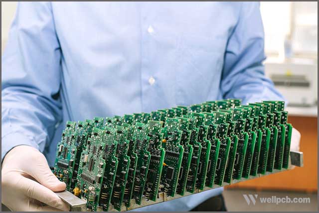
Mass Production
Before mass production became popular, most goods’ creation was highly reliant on initially making an order. However, when mass production developed and got perfected, most companies saw the advantages or benefits of producing goods in large quantities. In other words, manufacturing products in bulk reduces manufacturing costs. It is cheap to manufacture products in mass instead of making individual parts where economies of scale come in.
The same is true when it comes to the manufacture of multilayer printed circuit boards. If you want to lower your manufacturing costs, you need to manufacture your printed circuit boards in mass. This way, you will be reducing or minimizing the total expenditure spent on producing goods per the units manufactured.
Limit the Number of Geometries
If you desire to lower your multilayer printed circuit boards’ manufacturing cost, you must ensure that you reduce the geometries. Geometries do describe dielectric substrates details, reference planes, and traces within a printed circuit board stack-up.
If you choose to use or have larger geometries, such will bring about higher prices, especially in terms of the printed circuit board’s overall quantity. While larger geometries will bring about higher yields, you must be ready to spend more on your multilayer printed circuit boards.


Adherence to Recommended Tolerance
Even though tight tolerances, especially for the thickness of the printed circuit board, can bring about high-performing printed circuit boards, you need to be aware that such can raise the cost of your multilayer printed circuit board during the manufacturing phase.
Therefore, as a customer looking to lower your multilayer printed circuit board manufacturing costs, it is better if you go only for tight tolerances that will benefit the printed circuit board’s design and performance. Otherwise, it’s good to restrict the thickness of your board to tolerances. You need to adhere to the recommended tolerances to ensure that your manufacturing costs come down.

Maintain Enough Spacing Between Copper Layers
More than half ounce copper materials on the inner layers of the printed circuit board and close to 1 oz of copper found on the outer layer of printed circuit board increases the cost of manufacturing printed circuit boards significantly.
To ensure that you substantially minimize your multilayer printed circuit boards’ manufacturing costs, you need to ensure that you maintain enough spacing between the copper materials. To ensure that you get to lower your multilayer printed circuit boards’ costs, you may have to go direct your manufacturer to use thick copper. If the spacing between the copper materials is far from each other, it means that you’ll have to use plenty of components, an aspect that will increase the cost of manufacturing your printed circuit boards go high.

Multilayer PCB Manufacturing– Drill Size
When manufacturing printed circuit boards, the type of machine or equipment used to drill holes on the printed circuit board matters a lot. While high speeds and flexibility are some of the most significant advantages of laser drilling machines, you need to be aware that using these types of devices will see your manufacturing costs rising.
If you want to significantly minimize the manufacturing costs associated with creating your multilayer printed circuit board, consider using a nominal drill size instead of using a laser drilling machine, unless laser is the only viable option. Larger hole diameters are highly preferable when designing multilayer printed circuit boards as they demand less precision, especially during multilayer PCB fabrication. Additionally, such would see you lowering your Multilayer PCB Manufacturing costs.

Multilayer PCB Manufacturing– PCB Material Selection
Lastly, the choice of material used in the manufacture of a printed circuit board, especially multilayer printed circuit boards, invariably affects the production costs. Some factors that impact the selection of materials include temperature reliability, thermal reliability, signal performance, heat transfer, and mechanical properties, to mention but a few.
As a rule of thumb, those operations that involve high frequencies will demand high-grade materials. If you are on a budget and want to minimize your multilayer printed circuit board manufacturing costs, then it is advisable to select cost-effective materials that are suitable for your application. If you go for high-end equipment and require exceptional surface finish on your final product, then you must be prepared to handle the high production costs associated with such a procedure.
Always go for ordinary materials used in the manufacture of printed circuit boards to save some costs.

Summary
A trusted multilayer printed circuit board manufacturer always provides helpful suggestions on how to go about saving manufacturing costs without sacrificing the functionality or quality of the board. WellPCB is a reliable manufacturer helping our customers in all considerations.
Besides possessing exceptional multilayer board manufacturing experience, we have strict testing procedures aimed at ensuring that the avoidance of design errors. For more than a decade and counting, we have been assisting our customers with high-quality Multilayer PCB Manufacturing, prototyping, and assembly services at some of the most affordable costs.
If you have multilayer printed circuit board requirements or need information on how to go about saving your manufacturing costs, feel free to contact us for more details. We at WellPCB highly respect non-compete and the non-disclosure agreements, and we will ensure to keep all your files and any other document confidential.


