Contents
Preparing a Multilayer PCB
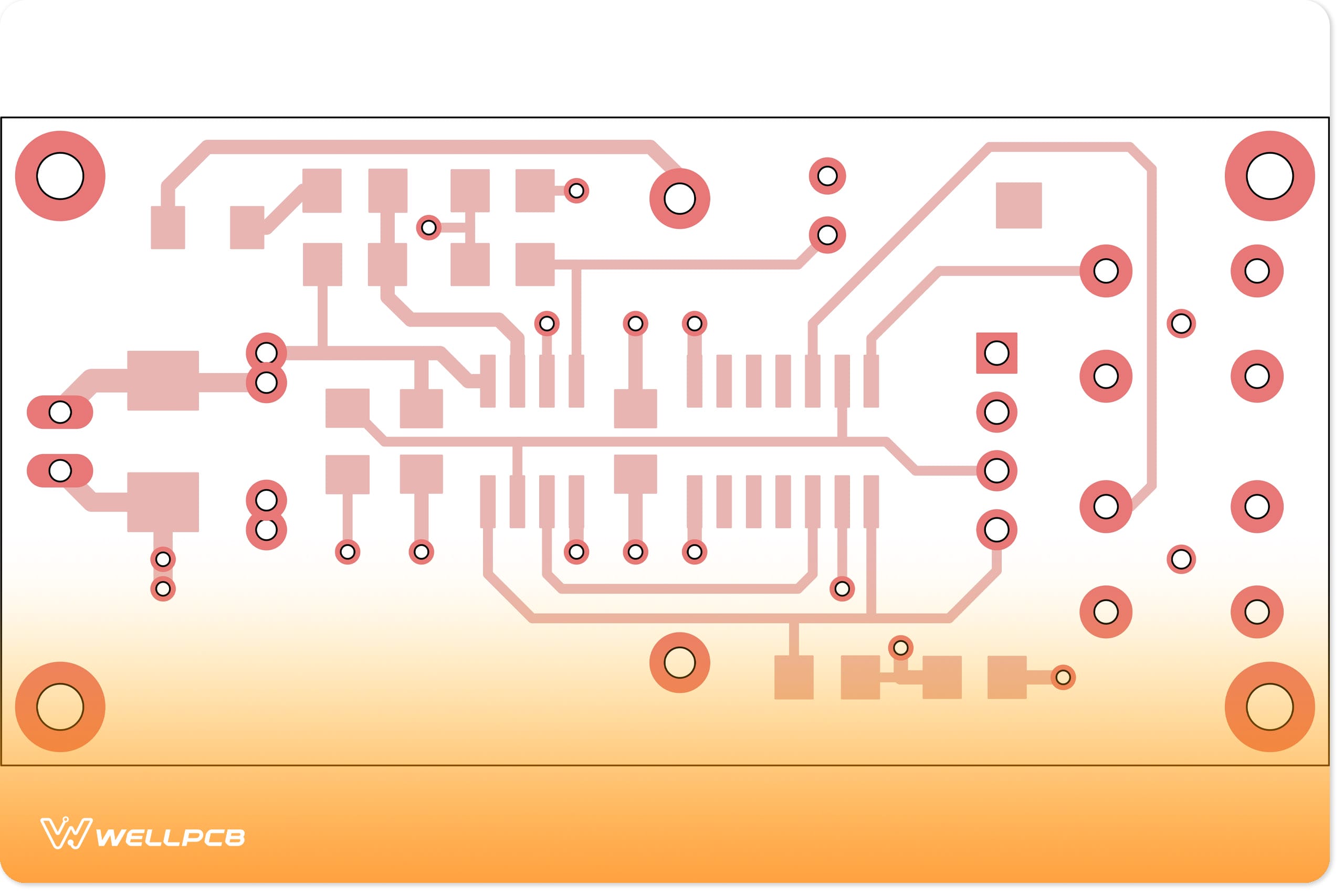
Every professional PCB design starts with creating the layout using specialized software. This process typically generates Gerber files, which define the PCB’s layers (such as copper traces and solder masks), and drill files, which specify the locations and sizes of holes for components and vias. Both file types are essential for PCB fabrication.
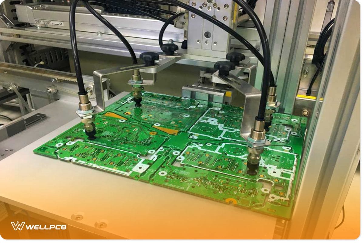
An automated pick-and-place robot is then used to assemble the onboard electronics.
For 32-layer printed circuit boards, assembly details are not only specified in the usual Bill of Materials (BOM) in PCB design files. A separate file with assembly instructions must accompany the software design files.
Technique Behind 32-Layer Printed Circuit Boards
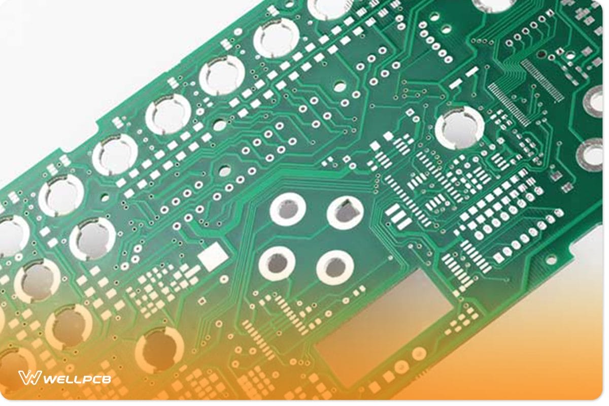
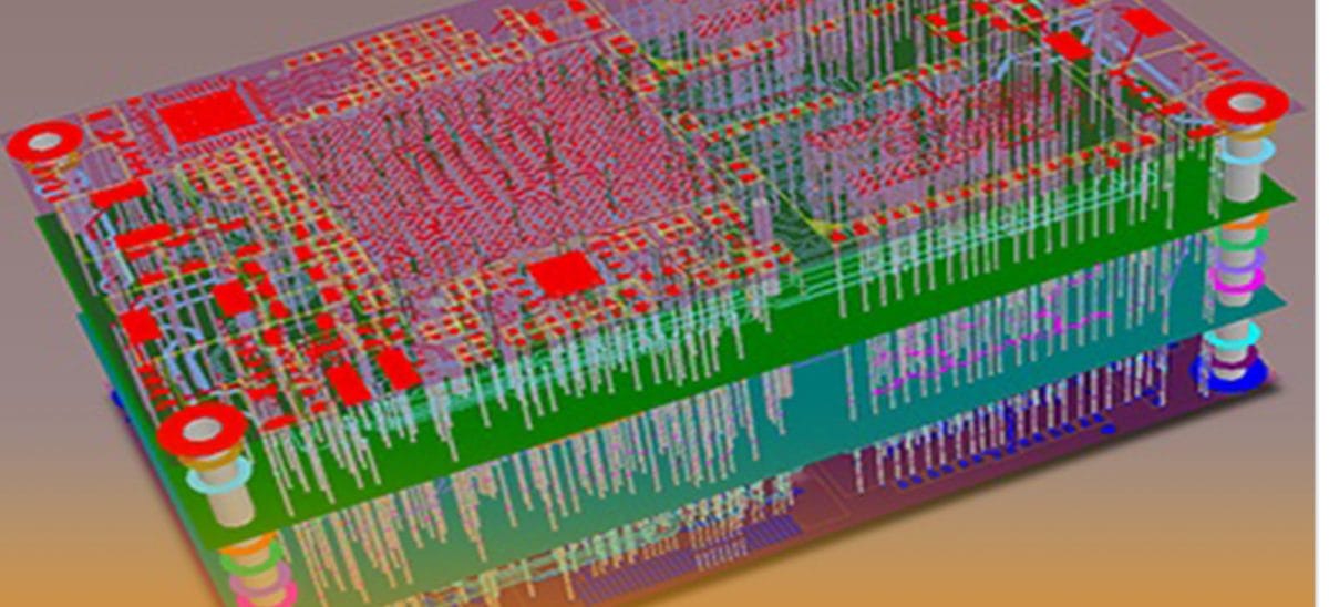
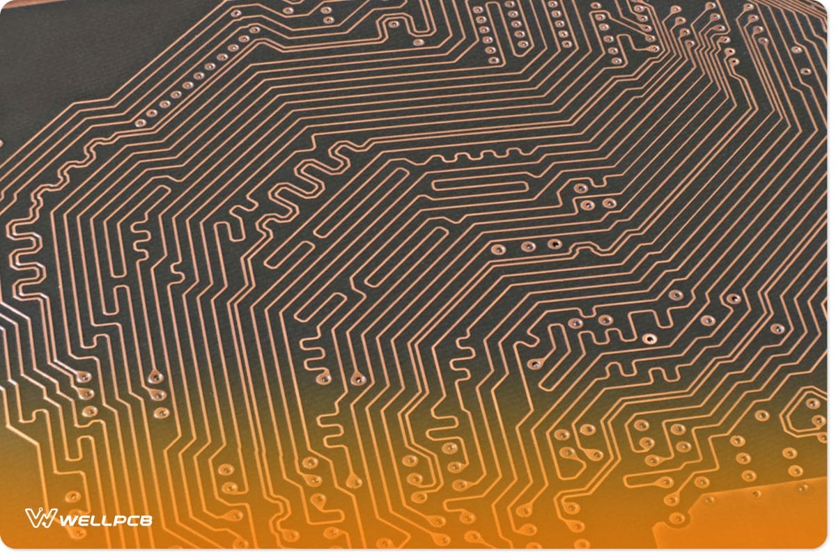
Manufacturing a 32-layer PCB involves constructing a stack-up of multiple PCB layers. This is achieved by sandwiching multiple double-layer PCBs with insulating fiber-epoxy layers, known as prepreg, between them. As such, the double-layer PCB is the basic building block for any multilayer PCB.
This two-sided PCB fabrication technique, with advanced machinery to handle the added complexity, makes it possible to fabricate 32-layer—or even 50-layer—PCBs.
32-Layer Printed Circuit Boards Applications
Why do we need 32-layer or 50-layer PCBs?
The primary reason is to efficiently embed all the required system electronics into a compact PCB. While component assembly is typically limited to the top and bottom layers, multilayer PCB components can be placed within the stack-up.
Applications in the aerospace industry are a prime use case for these complex PCB designs.
In aerospace systems, the target is to have as little or no electromagnetic emissions. Properly organizing a PCB during the design phase significantly reduces these emissions.
Each layer is typically dedicated to a certain function to avoid potential conflict with other layers. For instance, the middle layers often serve as supply power planes, while the top and bottom layers are reserved for component placement.
Conclusion
A 32-layer printed circuit board is a sophisticated and highly functional component that’s essential for advanced electronic applications. Its meticulous design and advanced manufacturing techniques ensure that these PCBs meet the strict requirements of industries like aerospace, where reliability and performance are non-negotiable.
Understanding the intricacies of multilayer PCB fabrication empowers designers and engineers to create more efficient, compact, and high-performing systems. As technology advances, the demand for such cutting-edge PCBs will continue to grow, making knowledge and expertise in this area invaluable.
For expert PCB fabrication, including complex multilayer designs, contact WellPCB. Our team specializes in precision manufacturing to meet your most demanding requirements, ensuring top-quality results for every project.
FAQ
What is a 32-layer PCB?
A 32-layer PCB is a multilayer printed circuit board comprising 32 layers of copper and insulating material, all laminated together. It is designed for use in advanced and complex electronic systems.
What are 32-layer PCBs used for?
These PCBs are commonly used in industries like aerospace, telecommunications, and high-density electronic systems. They are ideal for applications requiring high performance, compact design, and low electromagnetic interference (EMI).
How are 32-layer PCBs made?
They are manufactured by stacking and laminating multiple double-sided PCBs with layers of prepreg (an insulating fiber-epoxy material). Advanced machinery is used to achieve the required precision and complexity.