
Contents
- 1 P.C.B. Assembly New Project
- 1.1 I. WellPCB P.C.B. Assembly New Project—INTRODUCTION
- 1.2 II.WellPCB P.C.B. Assembly New Project-–METHODS OF POWER FACTOR CORRECTION (P.F.C.)
- 1.3 III.COMPONENTS, FUNCTIONAL BLOCK DIAGRAM, AND SCHEMATIC DIAGRAM
- 1.4 IV. WellPCB P.C.B. Assembly New Project—METHODOLOGY
- 1.5 V.Interfacing of Microcontroller to LCD and Relay Driver I.C.E. P.C.B. Assembly 3D View and P.C.B. Design
- 2 WellPCB P.C.B. Assembly New Project–P.C.B. Assembly 3D view
- 3 P.C.B. Design
- 4 PICTORIAL VIEW OF SYSTEM WITH IMPROVED POWER FACTOR.
P.C.B. Assembly New Project
I. WellPCB P.C.B. Assembly New Project—INTRODUCTION
Any motor that operates on alternating current requires apparent power, which is an addition of active and reactive power.
Dynamic control is the power that is consumed by the load. Reactive power is the power demanded by the amount and returned to the power source.
The simplest way to specify the power factor is ¯POWER FACTOR, the ratio between the sound (right) power whose unit is K.W. to the total (apparent) power whose unit is K.V.A. consumed by A.C. electrical equipment or motor‖.
Power factor measures how effectively electrical power is used to perform valuable Work. The ideal power factor is unity or one.
If the power factor is less than one, excess energy is required to perform or achieve this Bill Of Materials (B.O.M.) of a P.C.B. get fitted aboard. P.C.B. assembly project actual work.
A. Advantages of power factor improvement
Benefits that can be achieved by employing the proper power factor correction scheme are:
1. Efficiency increases due to the reduction of power consumption.
2. Due to reduced power consumption, there will be fewer greenhouse gases
3. Reduction of electricity bills
4. Extra K.V.A. available from the same existing supply
5. Reduction of I²R losses in transformers and distribution equipment
B. The idea to improve the power factor
The basic idea of this Bill Of Materials (B.O.M.) of a P.C.B. gets fitted aboard. P.C.B. assembly project for power factor correction of a motor or circuits, we have to connect a capacitor in parallel with the device with a low power factor.
One of the traditional methods for power factor correction is static-type compensation, in which fixed-type capacitors are used for power factor correction.
However, in this case, Care should be taken when applying power factor correction star/delta type control so that the capacitors are not subject to rapid on-off conditions.
C. Working of Capacitors
By representing active power & reactive power at the sides of the right angle, we can determine the apparent authority from the right triangle rule:
(K.V.A.)² = ( KW)²+ (KVAR)²
To reduce the K.V.A., the total current requirement for any given load, one must shorten the line representing the KVAR.
This is precisely what capacitors do. The ratio of actual power to apparent power is usually expressed in percentages and is called the power factor.
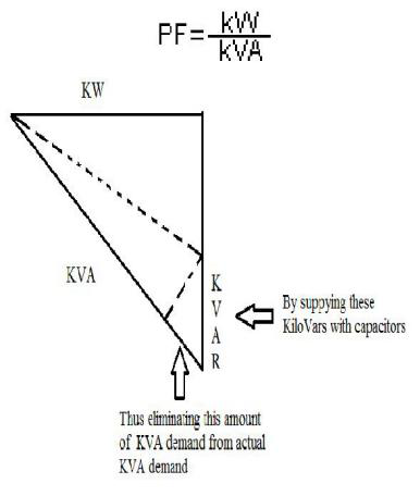
Fig-1. Power Triangle
II.WellPCB P.C.B. Assembly New Project-–METHODS OF POWER FACTOR CORRECTION (P.F.C.)
A. Static compensation
In this method for power factor improvement, static capacitors are connected in parallel with the device, which works on low power factors.
These fixed capacitors provide a maximum current which eliminates the lagging component of load current and improves the power factor.
B. Synchronous condenser
When a synchronous motor operates at no load and over-excited conditions, it is called a synchronous condenser.
A synchronous condenser is overexcited; it provides a maximum current and works like the capacitor of the P.C.B. assembly project.
When a synchronous condenser is connected across supply, it gives a leading current and partially eliminates reactive components, thus improving the power factor.
III.COMPONENTS, FUNCTIONAL BLOCK DIAGRAM, AND SCHEMATIC DIAGRAM
A. P.C.B. Assembly project Main components
The main components used in this scheme for automatic power factor correction using a microcontroller include the following elements.
- Auxiliary Power Supply: Transformer
Bridge rectifier
Voltage regulator IC 7805
2.Microcontroller(AT-megaA8)
3. LCD Display
4. Capacitor Bank
5. Potential transformer & current transformer
6. Relay & relay driver I.C.
7. Zero Cross Detector
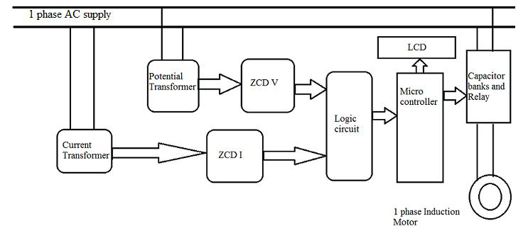
B. Functional Block Diagram
This P.C.B. assembly project detects zero crossings of voltage and current waveform from the line by Z.C.D. from P.T. and C.T., respectively.
Depending upon the phase difference between voltage and an existing microcontroller sends out the signal to switch on the capacitor through relay driver I.C. and improves power factor.
C. Schematic Diagram
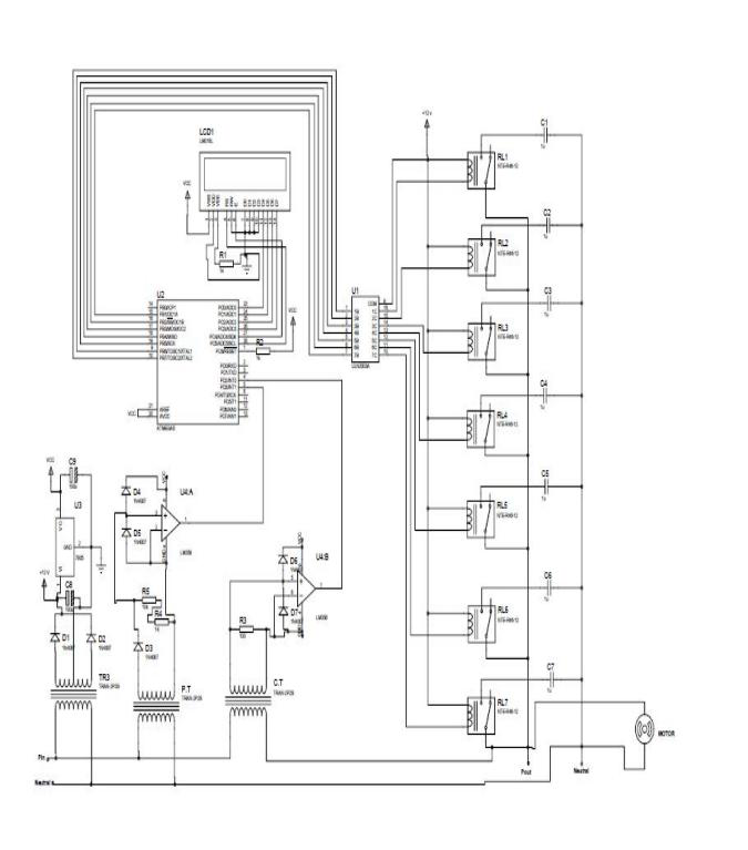
Fig-3 Schematic Diagram of System
D. Description of Microcontroller: AVR AT mega 8L
The Atmel ATmega8 is a powerful microcontroller that provides a highly flexible and cost-effective solution to many embedded control applications. The ATmega8 is a low-power CMOS 8-bit microcontroller based on the AVR RISC architecture.
By executing powerful instructions in a single clock cycle, the ATmega8 achieves throughputs approaching 1 MIPS per MHz, allowing the system designer to optimize power consumption versus processing speed.
The A.V.R. core combines a rich instruction set with 32 general-purpose working registers. All 32 entries are directly connected to the Arithmetic Logic Unit (ALU), allowing two independent records to be accessed in one instruction executed in one clock cycle.
The ATmega8 A.V.R. is supported with a full suite of program and system development tools, including C compilers, macro assemblers, program debugger /simulators, In-Circuit Emulators, and evaluation kits.
Features:
1.8K bytes of In-System Programmable Flash with Read-While-Write capabilities.
2.512 bytes of EEPROM, the 1K byte of SRAM.
3.23 general-purpose I/O lines.
4.32 general-purpose working registers.
5. Three flexible Timers/Counters with compare modes. Internal and external interrupts.
6. A serial programmable USART.
7. A byte-oriented Two-wire Serial Interface.
8.A 6-channel A.D.C. (eight channels in TQFP and QFN/MLF packages) with 10-bit accuracy.
9. A programmable Watchdog Timer with Internal Oscillator
E. Pin Configuration
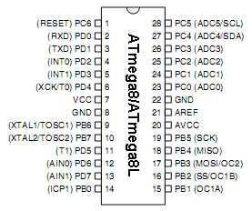
Pin Descriptions
- VCC- Digital supply voltage.
- GND- Ground.
- Port B (PB7-PB0)-Port B is an 8-bit bi-directional I/O port with internal pull-up resistors (selected for each bit).
- Port C (PC5-PC0) is a 7-bit bi-directional I/O port with internal pull-up resistors (selected for each bit).
- Note that the electrical characteristics of PC6 differ from those of the other pins of Port C. If the RSTDISBL Fuse is unprogrammed, PC6 is used as a Reset input.
- PC6/RESET- If the RSTDISBL Fuse is programmed, PC6 is used as an I/O pin. A low level on this pin for longer than the minimum pulse length will generate a Reset, even if the clock is not running. Shorter pulses are not guaranteed to make a Reset.
- Port D (PD7-PD0)-Port D is an 8-bit bi-directional I/O port with internal pull-up resistors (selected for each bit).
- RESET-Reset input. A low level on this pin for longer than the minimum pulse length will generate a reset, even if the clock is not running. Shorter pulses are not guaranteed to make a reset.
- AREF- AREF is the analog reference pin for the A/D Converter.
- AVCC-AVCC is the supply voltage pin for the A/D Converter, Port C (3-0), and A.D.C. (7-6). It should be externally connected to VCC, even if the A.D.C. is not used.
- If the A.D.C. is used, it should be connected to VCC through a low-pass filter. Port C (5-4) uses VCC’s digital supply voltage. 9.
- ADC7-6 In the TQFP and QFN/MLF package, ADC7-6 serves as analog inputs to the A/D converter. These pins are powered from the analog supply and serve as 10-bit A.D.C. channels.
IV. WellPCB P.C.B. Assembly New Project—METHODOLOGY
The methodology on which my paper-based is consisting of three main parts.
A. Auxiliary power supply
A bridge rectifier connected across the mainline converts A.C. signal to D.C. A capacitor is attached to the output of the rectifier to get pure D.C.
The production of the bridge rectifier is +12V. Still, as the microcontroller works on +5V, this bridge rectifier’s output is further given to IC 7805(Voltage regulator I.C.), which offers a fixed output voltage of +5V.
A capacitor is connected at IC 7805 to get pure D.C. voltage (remove unwanted ripples).
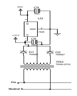
Fig-5. Auxiliary Power Supply
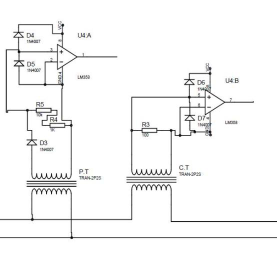
B. Zero cross detector (Z.C.D.)
The current and voltage signal is measured from the main A.C. line using the current transformer and potential transformer, respectively.
The output of these C.T. and P.T.s are given to Op-Amp LM 358. The combination of potential transformer and OP-Amp forms zero cross detector (Z.C.D. V) also mix of current transformer, and OP-Amp styles zero cross detector(ZCD I).
these zero-cross sensors individually convert both current and voltage waveforms to square wave and detects zero crossings of voltage and current.
C. Capacitor and relay matrix
Depending upon zero crossings of voltage and current wave microcontroller either switches on or switches off the required number of capacitors through electromagnetic relays. And the power factor is shown on the LCD for the various loads.
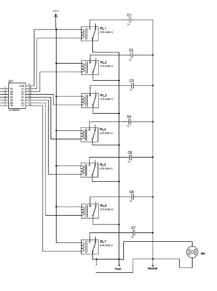
Fig-7 Connections of Capacitor & Relay Matrix Circuit
D. Flow Chart
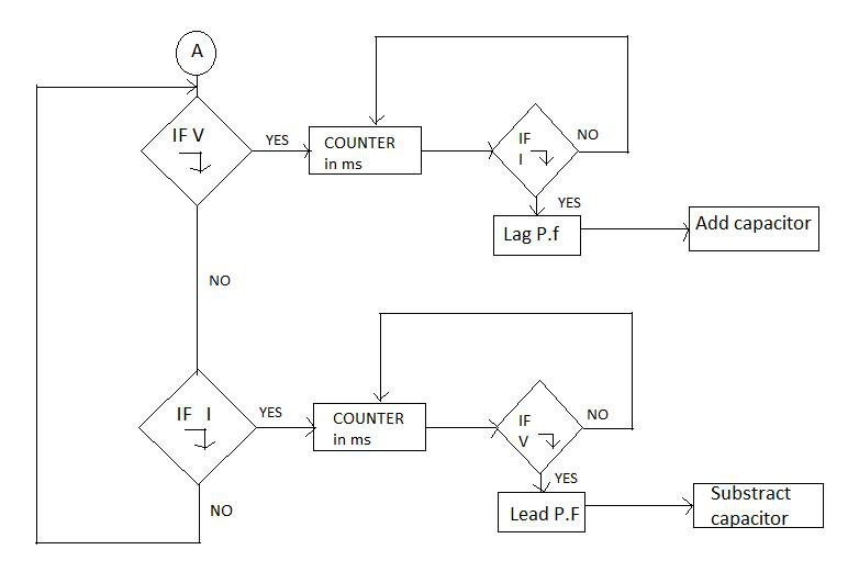
Fig-9. Flow Chart for system
The microcontroller first detects whether the first voltage edge is falling or the new side. Depending upon this logic, it detects whether the power factor is lagging or leading; accordingly, it switches on or off the number of capacitors to improve the power factor.
V.Interfacing of Microcontroller to LCD and Relay Driver I.C.E. P.C.B. Assembly 3D View and P.C.B. Design
WellPCB P.C.B. Assembly New Project–P.C.B. Assembly 3D view
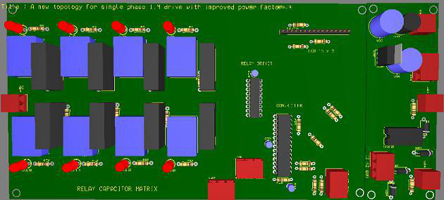
Fig-10 Proposed 3-D View of System.

P.C.B. Design
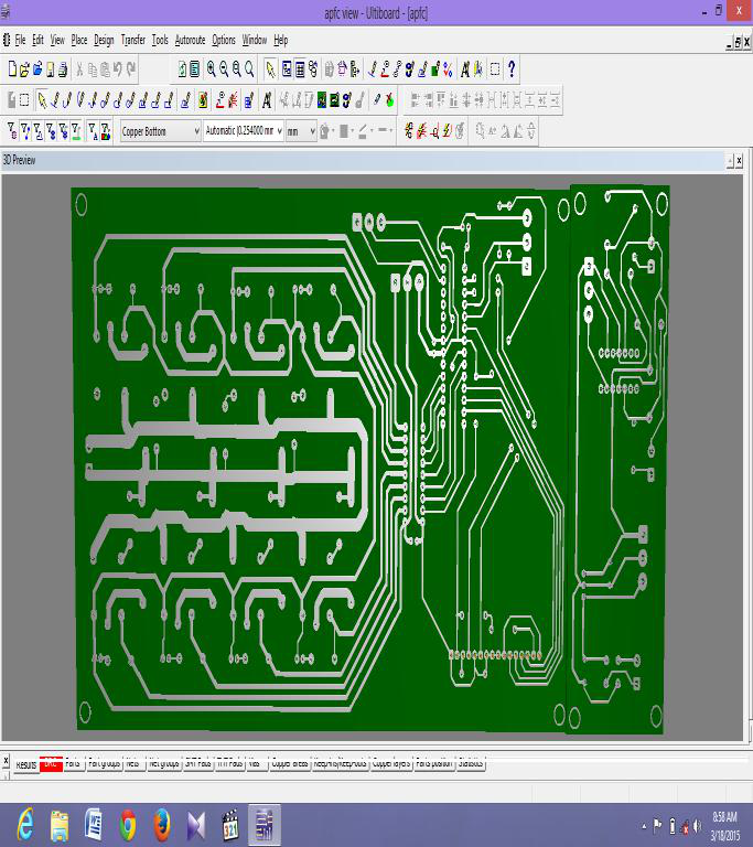
Fig-11. P.C.B. Design of System
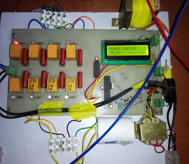
VI.PICTORIAL VIEW OF SYSTEM A LAGGING POWER FACTOR
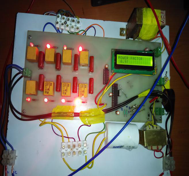
PICTORIAL VIEW OF SYSTEM WITH IMPROVED POWER FACTOR.
VII. WellPCB P.C.B. Assembly New Project—CONCLUSIONS
This paper deals with the advanced power factor correction method by using the microcontroller. As the Switching of capacitors is done automatically; hence, we get a more accurate result.
Power factor correction techniques make the system stable, and due to the improvement in power factor, its efficiency also increases.
Power factor correction scheme can be applied to industries, power systems as well as in household purposes.
The use of microcontrollers reduces costs. Using a microcontroller, multiple parameters can be controlled, and the use of other hard wares such as the timer, RAM, R.O.M., and input-output ports reduces. Before APFC Circuit insertion
VIII. FUTURE ENHANCEMENTS
The automotive power factor correction using capacitive load banks is very efficient as it reduces the cost by decreasing the power drawn from the supply.
As it operates automatically, the workforce is not required, and this Automated Power factor Correction using capacitive load banks can be used for the industry’s purpose in the future.
In the end, P.W.M. techniques can be employed in this scheme. Along with power factor correction, speedd control can be done in the future.
In the future, Work can be done for harmonics reduction.
Designed by: Usman_Ali_khan
