
Battery Management IC

Boost Converter

USB Connectors

MOSFETs

Capacitors

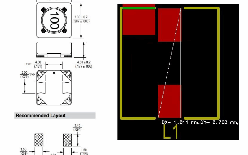
Inductors

Resistors

Protection Circuits

LEDs / Display

Thermal Sensors

Certified Quality and
Process Control

Engineering Expertise in
Power Bank Circuit Design

Verified Material
Sourcing

Testing to Performance Standards

Fast Quoting and Responsive Production

Cross-Section and X-ray Analysis
Thermal Cycling and Thermal Shock Testing

FR-4

CEM-1

Polyimide

Aluminum

Submit Your PCB Design
Upload your Gerber files or use our easy online PCB design tool to create your board layout. Make sure your files are complete and correctly formatted to ensure smooth processing and production accuracy.

Select Your PCB Specifications
Customize your order by choosing the technical specifications—number of layers, board dimensions, thickness, copper weight, solder mask color, surface finish, and more. Our intuitive interface helps you configure everything based on your project’s needs.

Get an Instant Quote
Once your design and specs are in place, you'll receive a transparent, instant quote. Pricing updates in real time as you modify options, so you can adjust your selections to match your budget before placing the order.

Confirm Order & Make Payment
Review your entire order for accuracy, including file previews and selected specs. After confirmation, proceed to secure checkout and choose your preferred payment method. You’ll receive an email confirmation with order details.

Production & Delivery
Your PCB moves into production immediately. We’ll keep you updated throughout the manufacturing process. Once completed, your boards are carefully packed and shipped to your door, with tracking information provided for your convenience.

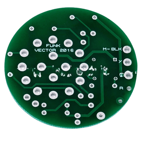
Standard Power Bank Circuit Board
These power bank circuit boards support single or dual USB output with common voltage profiles such as 5V 1A and 5V 2A.
They use FR-4 substrates designed for low to mid-capacity mobile power banks (e.g. 5000mAh to 10000mAh).

Fast Charging Power Bank Modules
Designed for higher performance, these modules support protocols like PD, QC 3.0, and proprietary fast charging standards.
Outputs include 20W fast charging, 45W, 65W, and even 100W for laptops and power-intensive devices. Interfaces often include USB-C, Type-C USB, and dual USB 5V 2.4A.
Power Bank Circuit Boards for 18650 Cells
These power bank PCBs are compatible with single or multi-cell 18650 battery packs, often including balancer circuits for charge equalization.
They offer flexible outputs (5V, 9V, 12V) and can incorporate circuit protection for overcharge, discharge, and thermal faults.
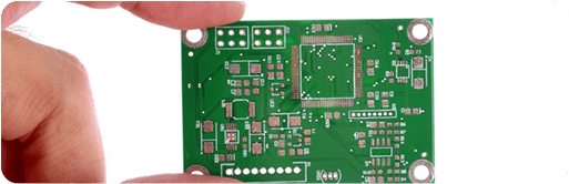
Custom and Advanced Module Boards
Advanced power bank modules feature integrated microcontrollers or smart ICs like IP5328P, enabling adaptive voltage outputs, optimized energy conversion, and additional functions such as LED display indicators, charging and discharging monitoring, and boost converter step-up power regulation.
These designs support DIY power bank projects and high-capacity configurations up to, 20000mAh or higher.


Hommer Zhao
Founder and Chief Editor – Hommer Zhao
Welcome! I’m Hommer Zhao, the founder and Chief Editor of WellPCB. With years of experience in the PCB industry, I’m committed to making sure our content is both accurate and helpful. We’re proud to serve a growing community of over 4,000 customers worldwide, and our goal is to provide you with the best resources and support. Your satisfaction is our top priority, and we’re here to help you every step of the way!

Jesse Holland
Technical Manager – Jesse Holland
Hi, I’m Jesse Holland, an Engineer and Technical Manager at WellPCB. With years of experience in PCB design and engineering, I’m here to ensure that every project we work on meets the highest technical standards. I lead our team, focusing on precision and innovation, collaborating closely with clients to provide tailored solutions and expert guidance. Whether you’re facing a complex design challenge or need advice on technical aspects, I’m here to ensure your project is a success from start to finish.

Nathan Jensen
Purchasing Manager – Nathan Jensen
Hi, I’m Nathan Jensen, the Purchasing Manager at WellPCB. I’m responsible for sourcing the best materials and components to ensure our products meet the highest quality standards. With my extensive experience in procurement, I work closely with suppliers to secure reliable and cost-effective solutions while maintaining strong relationships to support our operations. I aim to ensure every project runs smoothly by providing the resources needed to deliver on time and to your satisfaction.

Emma
Sales Manager – Emma
Hey, I am Emma, sales manager at WellPCB. I studied electronic science and technology at university and have served customers for PCB and PCB Assembly service for several years.
I enjoy communicating with customers and our technicians to solve problems, and customers always say, "It's great to have you onboard".
It is my pleasure and honour to be helpful. Contact me now, and you'll know.

Bella and Cassiel
Sales Representatives – Bella and Cassiel
We’re Bella and Cassiel, your dedicated sales representatives at WellPCB. With our extensive knowledge of the PCB industry, we’re here to provide exceptional service and support. We take the time to understand your unique needs and are always ready to offer tailored solutions and advice. Whether you need product recommendations, assistance with your orders, or simply have a question, we’re here to ensure your experience is smooth and seamless at every step.

Mandy and Wendy
Sales Representatives – Mandy and Wendy
We’re Mandy and Wendy, your friendly sales representatives at WellPCB. Passionate about helping our customers, we bring a wealth of experience in the PCB industry to provide you with the best solutions and service. We take pride in building strong relationships with our clients, understanding their specific needs, and offering personalised support to ensure their satisfaction. Whether you’re looking for advice, product information, or assistance with any part of your order, we’re here to make your experience as smooth and efficient as possible.
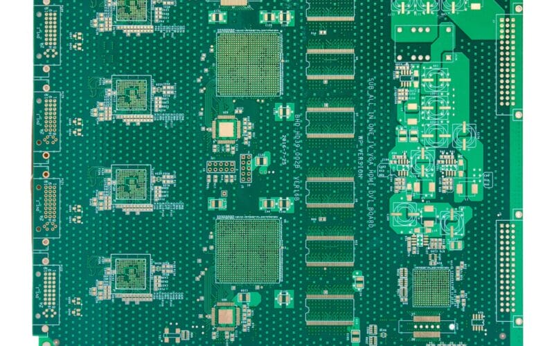
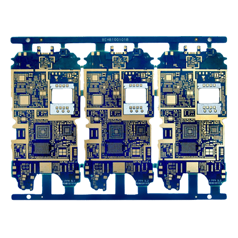
PCB Manufacturing
PCB Specifications
- Layers: 8
- Board Thickness: 1.8mm
- Min. Line Width/Space: 3/3.5 mil
- Min. Hole Size: 0.2mm
- Min. Distance from Hole to Line: 0.13mm
- Inner Layer Copper: Hoz
- Outer Layer Copper: 1oz
- Surface Finish: Immersion Gold
The final board met all mechanical and electrical tolerances and passed electrical testing with 100% yield. This project shows our capabilities to handle complex, high-density multilayer PCBs with tight tolerances and strict quality standards.
PCB Assembly
Project Details
- Service Type: PCB Assembly
- Location: Italy
- Client Type: PCB Design Company
- Total Units: 20
- Lead Time: Rapid turnaround for prototyping
- Assembly Type: SMT+THT mixture assembly
Our experienced production team worked closely with the client to verify the BOM, optimize the stencil and the board’s layout design. We completed and delivered 20 fully assembled units within the expected lead time, allowing the client to avoid delays and meet their customers’ delivery window. This case highlights our capabilities to support global clients with flexible, low-volume PCB assembly solutions.
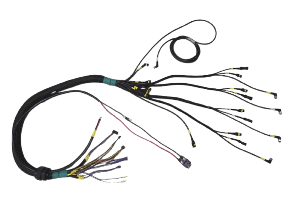
Wire Harness
Project Details
- Service Type: Custom Automotive Wire Harness
- Location: New York, USA
- Client Type: Auto Repair Shop
- Quantity: 10,000 Units
Our team followed strict quality guidelines throughout production, using automotive-grade connectors and insulation materials. The order was completed on schedule with no reported defects, supporting the client’s rollout without interruption. This case shows our comprehensive capabilities in large-scale production, customized solutions, quality control and efficient delivery.

Order options
What customers say
Their engineers reviewed our power bank pcb assembly stackup and caught an issue early.
Turnaround on the power bank pcb assembly order beat the quoted lead time.
Easy to reach and proactive on status for our power bank pcb assembly.
Our go-to for power bank pcb assembly now; reorders are always reliable.
They flagged a hidden short on our power bank pcb assembly during assembly inspection — genuinely thorough people.