Problems And Considerations In PCB Design It’s Here

July 2, 2021
by Emma Lu

PCB Design devices demonstrate the effect of material polarization due to mechanical stress or deformation of the material and vice-versa. This phenomenon can be exploited to get sensor data on temperature, mechanical pressure, vibration etc. Or using the opposite mechanism to control actuators.

Negative effects generated by or acting into analog signals. It should be taken carefully into consideration. When designing the PCB board and selecting its assembly components.

This article will describe in short. Some of those issues and solutions are commonly used to avoid or minimize the negative effects.

Problems and Considerations in PCB Design

First of all, it is a common practice to connect and carry analog signals to be as separated. As much as possible from the regions in the PCB design board. Where digital signal connections take place.

On the other hand, analog signals are sensitive to this kind of radiation, resulting in interference between signals and making the whole circuit dysfunctional in the worst case.

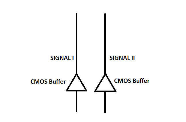
Besides that, two wires carrying digital signals can result in loss of performance as well. This effect is caused because of the capacitance generated between two wires carrying current. As illustrated in the left figure.

C is the capacitance created in the dielectric region between the two signals after analog signals are taken from the inputs of piezotronic sensors. They are converted into digital using ADC’s. Current continually.  Rapidly changes in the wire, thus generating inductance. This causes noisy currents in the other wire. One of the solutions commonly used is utilizing a CMOS Buffer Integrated Circuit. Which by letting all signals pass through the buffer. As illustrated in the right figure.

Problems and Considerations in PCB Design2.png
Problems And Considerations In PCB Design5

PCB Assembly Services

Kickstart Your Projects with Precision! Get PCB Assembly for Only $99—Limited Time Offer!

ORDER NOW

Problems And Considerations In PCB DesignOthers

Other common practices reduce coupling (transfer the energy from one wire to another. Through the changing electromagnetic field). These are the routes of signals as in the PCB design. Using a whole layer in PCB. As ground helps reduce route lengths targeting ground at a minimal level.

PCB Assembly Services

Kickstart Your Projects with Precision! Get PCB Assembly for Only $99—Limited Time Offer!

ORDER NOW
Avatar photo
Emma Lu
Our professional engineering support saves our customers a lot of trouble and loss. >>>>>> After you place the order, our engineer will conduct technical reviews to make sure the parts can be mounted well/correctly on the boards. We will check if the component packages match well with the Gerber footprints, if the part numbers you provided match well with the descriptions, and if the polarity is clearly marked. >>>>> When your design is ready, please send your Gerber and BOM so we can quote and start!